Note: Descriptions are shown in the official language in which they were submitted.
CA 02652060 2008-11-12
WO 2008/066569 PCT/US2007/011612
HERMETIC CHAMBER WITH ELECTRICAL FEEDTHROUGHS
FIELD OF THE INVENTION
[0001] The present invention relates to micromachinable, pico- to nanoliter-
volume, hermetic
packaging that incorporates reliable electrical feedthroughs, and sensors
configured utilizing the
same, all of which are intended to perform reliably in harsh and biological
environments.
BACKGROUND OF THE INVENTION
[0002] Over the past 20 years, advances in the field of microelectronics have
enabled the
realization of microelectromechanical systems (MEMS) and corresponding batch
fabrication
techniques. These developments have allowed the creation of sensors and
actuators with
micrometer-scale features. With the advent of the above-described capability,
heretofore
implausible applications for sensors and actuators are now significantly
closer to commercial
realization.
[0003] In parallel, much work has been done in the development of pressure
sensors. Pressure
sensors are disclosed, for example, in U.S. Patent No. 6,111,520, issued
August 29, 2000; U.S.
Patent No. 6,278,379, issued August 21, 2001; U.S. Patent No. 6,855,115,
issued February 15,
2005; U.S. Patent Application Serial No. 10/054,671, filed January 22, 2002;
U.S. Patent
Application Serial No. 10/215,377, filed August 7, 2002; U.S. Patent
Application Serial No.
10/215,379, filed August 7, 2002; U.S. Patent Application Serial No.
10/943,772, filed September
16, 2004; and U.S. Patent Application Serial No. 11/157,375, filed June 21,
2005; U.S. Patent
Application Serial No. 11/314,696 filed December 20, 2005; and U.S. Patent
Application Serial
No. 11/402,439 filed April 12, 2006 all of which are incorporated herein by
reference.
[0004] In particular, absolute pressure sensors, in which the pressure
external to the sensor is
read with respect to an internal pressure reference, are of interest. The
internal pressure reference
1.
CA 02652060 2008-11-12
WO 2008/066569 PCT/US2007/011612
is a volume within the sensor, sealed, which typically contains a number of
moles of gas (the
number can also be zero, i.e. the pressure reference can be a vacuum, which
can be of interest to
reduce temperature sensitivity of the pressure reference as known in the art).
The external
pressure is then read relative to this constant and known internal pressure
reference, resulting in
measurement of the external absolute pressure. For stability of the pressure
reference and
assuming the temperature and volume of the reference are invariant or
substantially invariant, it is
desirable that the number of moles of fluid inside the reference does not
change. One method to
approach this condition is for the reference volume to be hermetic.
[0005] The term hermetic is generally defined as meaning "being airtight or
impervious to
air." In reality, however, all materials are, to a greater or lesser extent,
permeable, and hence
specifications must define acceptable levels of hermeticity. An acceptable
level of hermeticity is
therefore a rate of fluid ingress or egress that changes the pressure in the
internal reference
volume (a.k.a. pressure chamber) by an amount preferably less than 10 percent
of the external
pressure being sensed, more preferably less than 5 percent, and most
preferably less than 1
percent over the accumulated time over which the measurements will be taken.
In many
biological applications, an acceptable pressure change in the pressure chamber
is on the order of
1.5 mm Hg/year.
[0006] The pressure reference is typically interfaced with a sensing means
that can sense
deflections of boundaries of the pressure reference when the pressure external
to the reference
changes. A typical example would be bounding at least one side of the pressure
reference with a
deflectable diaphragm or plate and measuring the deflection of the diaphragm
or plate by use of,
among other techniques, a piezoresistive or a capacitance measurement. If the
deflection of the
diaphragm or plate is sufficiently small, the volume change of the pressure
reference does not
substantially offset the pressure in the pressure reference.
[0007] These approaches may require an electrical feedthrough to the hermetic
environment
(e.g., to contact electrodes inside the hermetic pressure reference), for
connection to outside
2.
CA 02652060 2008-11-12
WO 2008/066569 PCT/US2007/011612
electronics to buffer or transmit the signal. Alternatively, electronics may
be incorporated within
the reference cavity, requiring power to be conducted into the hermetic
environment. To maintain
stability of the pressure reference, these seals should also be hermetic,
resulting in the necessity to
develop a feedthrough technology for contacts through the cavity walls. As is
known in the art,
such feedthrough points are typically sites for failure of hermeticity. This
problem is further
exacerbated when miniaturizing the sensor, since the total volume of material
available for
hermetic sealing shrinks proportionally and the reliability of the feedthrough
is also greatly
reduced. In the limit of ultraminiaturized sensors, such as those producible
using
microelectromechanical systems (MEMS) technology, one of the major challenges
to enabling
the use of such devices in applications where they are physically connected to
other devices has
been the creation of reliable hermetic packaging that provides feedthroughs
that enable exchange
of power and information with external electronics.
[0008] Design criteria for ultra miniature packaging that overcomes the
aforementioned
shortcomings are as follows: The packaging must exhibit long term hermeticity
(on the order of
the life of the sensor, which in some cases can exceed tens of years).
Feedthroughs must be
provided through the hermetic package that do not introduce new or unnecessary
potential modes
of failure. The feedthroughs will constitute a necessary material interface,
but all other interfaces
can and should be eliminated. In other words, the number and area of material
interfaces should
be minimized to reduce the potential for breach of hermeticity. The materials
selected must be
compatible with the processes used to fabricate the package as well as
sufficiently robust to resist
deleterious corrosion and biocompatible to minimize the body's immune
response. Finally, the
packaging should be amenable to batch fabrication.
[0009] In the past, many methods for creating such hermetic packages have been
proposed.
One approach used in the past to create the pressure cavity is anodic bonding
to create a silicon-
to-glass seal. A borosilicate glass is required for this method. Another
technique utilized in the
creation of hermetic packages is eutectic bonding to create a silicon to metal
hermetic seal, e.g.
3.
CA 02652060 2008-11-12
WO 2008/066569 PCT/US2007/011612
Au to Si. Both of these bonding methods used to create the pressure cavity
introduce a large area
along the perimeter of the material interface of the pressure cavity package
which presents
opportunity for failure, e.g. through corrosion. These methods for creating
the pressure cavity do
not minimize the area of the material interface as is desirable. A desirable
improvement to the
construction of the pressure cavity would minimize the material interface to
the hermetic
electrical feedthroughs, and, even further, minimize the number and area of
material interfaces in
those feedthroughs.
[0010] Previous attempts to create hermetic feedthroughs also fall short of
the above-stated
requirements. Many prior art hermetic feedthroughs are too large and not
amenable to the
required miniaturization for pico- to nanoliter volume packaging achievable by
MEMS or similar
approaches. Furthermore, earlier attempts to create feedthroughs in pico to
nanoliter packaging
are prone to corrosion because of the materials used in construction or are
sufficiently
complicated that they introduce more material interfaces than are necessary. A
representative
feedthrough approach, known as a "buried" feedthrough, is illustrated in FIGS.
1-5. One method
for creating a buried feedthrough is as follows: a metal 10 is deposited onto
substrate 12 in a
predefined pattern, as shown in FIG. 1. An insulating layer 14 is deposited on
top of the metal
layer, as shown in FIG. 2, and this insulating layer 14 is polished to
planarize this surface. In FIG.
3 an etchant has been used to expose the metal layer at input and output sites
16, 18 for the
feedthroughs. In FIG. 4, another substrate 20 is bonded on top of this
structure, forming a
hermetic cavity 22. A eutectic bonding method is illustrated, which involves
the use of gold
deposits 24 interposed between the insulating layer 14 and the upper substrate
20 to bond the
upper substrate to the insulating layer. In FIG. 5 the upper substrate 20 is
machined to expose the
external feedthrough 18. An electrical conductor can now be connected to the
external
feedthrough 18, whereupon it is conducted through the metal 10 to the internal
feedthrough 16
and thus to a location within the hermetically sealed chamber 22.
4.
CA 02652060 2008-11-12
WO 2008/066569 PCT/US2007/011612
[0011] This prior art buried feedthrough suffers a number of disadvantages.
First, there are
numerous material interfaces: an interface 30 between the lower substrate 12
and the metal 10; an
interface 32 between the metal 12 and the insulating layer 14, an interface 34
between the
insulating layer 14 and the gold 24; and an interface 36 between the gold 24
and the upper
substrate 20, all of which create potential paths for infusion into or
effusion out of the hermetic
chamber 22. The creation of this buried feedthrough also introduces increased
processing steps.
Further, the insulating layer material is cited as being prone to corrosion in
certain environments,
e.g. the human body. Corrosion issues may be further exacerbated by the
application of electrical
bias to metal 10 which may be required in certain applications. Thus prior art
hermetic
feedthroughs fall short of meeting the constraints outlined above.
[0012] Also, many prior art attempts to provide pressure sensors utilize
silicon as a substrate
material. If the package is implanted in vivo, silicon is not an optimal
material choice. Silicon
invokes an undesirable immune response over other, more inert materials such
as fused silica. If
silicon is used, a coating must be applied to ensure biocompatibility. Such a
coating increases the
package size, thereby decreasing the benefits of miniaturization, and
introduces an undesirable
additional processing step in the manufacture of the package.
[0013] Additionally, prior art devices commonly employ the use of borosilicate
glass as part
of the pressure cavity. The ions in borosilicate glass constitute an impurity
in the glass. The
barrier to diffusion of water decreases as the purity of glass decreases. This
makes use of impure
glass undesirable in such applications.
[0014] Thus a need exists for hermetic pico to nanoliter packaging with
electrical
feedthroughs for use in biological environments, such packaging being
constructed of high-purity
materials and having a reduced number and area of material interfaces.
5.
CA 02652060 2008-11-12
WO 2008/066569 PCT/US2007/011612
SUMMARY OF THE INVENTION
[0015] The present invention comprises a micromachinable, hermetic, pico to
nanoliter-
volume pressure cavity. Such a pressure cavity utilizes high-purity materials
and provides reliable
electrical feedthroughs. The pressure cavity is constructed of a ceramic
material and is optionally
fused together so that there is no interface of material where two substrates
have been joined to
create a cavity. Furthermore, feedthroughs establishing electrical
communication within said
cavity are formed in at least one of the substrates. The feedthroughs
themselves are configured in
such a way that the number and area of material interfaces is minimized. Such
feedthroughs
constitute the only site for material interface in the sensor package, thereby
decreasing the
number of potential leak sites in and increasing the reliability of the
hermetic package. Pressure
cavities and sensors of the present invention are manufactured using
microelectromechanical
systems (MEMS) fabrication techniques, which allow creation of a device that
is small, accurate,
precise, durable, robust, biocompatible, and insensitive to changes in body
chemistry or biology.
[0016] The present invention further comprises a sensor that can be
incorporated into harsh
and biological environments. One example of such an environment is a medical
lead or catheter
implanted, acutely or chronically, into the human body. The sensor is
configured to measure one
or more physical properties such as pressure or temperature. Communication
between the sensor
and another device can be established by, e.g., using wires fixed to bonding
pads on the exterior
of the sensor packaging that are configured so that they are in electrical
contact with the hermetic
feedthroughs. As another example, the hermetic electrical feedthrough can have
a wire extending
from the feedthrough, and contact with the pressure cavity can be accomplished
via connection
with this wire. Devices in electrical communication with sensors according to
the present
invention may be either implanted or external to the body. Sensors of this
invention are
sufficiently small to allow for incorporation into medical leads or catheters
that are twelve French
or smaller, preferably six French or smaller, without causing abrupt changes
in geometry of the
lead or catheter, and require minimal power to perform their intended
function.
6.
CA 02652060 2008-11-12
WO 2008/066569 PCT/US2007/011612
[0017] In one embodiment of the invention, a wired sensor ascending to the
present invention
comprises a hermetic pressure cavity. The pressure cavity further comprises a
capacitor
configured so that the characteristic capacitance value of the capacitor
varies in response to a
physical property, or changes in a physical property, of a patient. The
electrodes of the capacitor
are substantially planar and are arranged substantially parallel to and spaced
apart from one
another. The pressure cavity has at least one deflectable region in mechanical
communication
with at least one of the capacitor electrodes. Additionally, electrical
feedthroughs are formed
through the substrate defining the pressure cavity and allow for the sensor to
receive power and
signals, and return information to either implanted or extracorporeal external
electronics.
[0018] In another embodiment of the invention, a wired sensor according to the
present
invention comprises a hermetic pressure cavity. The pressure cavity further
comprises a
Wheatstone bridge configured so that the resistance value of said bridge
varies in response to a
physical property, or changes in a physical property, of a patient. The
pressure cavity has at least
one deflectable region in mechanical communication with at least one of the
resistors comprising
the bridge. Additionally, electrical feedthroughs are formed through the
substrate and allow for
the sensor to receive power and signals, and return information to external
electronics. It is a
further aspect of this invention that only a portion of the Wheatstone bridge
be located within the
pressure cavity, the other portion being contained within external
electronics.
[0019] In yet another embodiment, a wired sensor further comprises on-board
(i.e., within the
sensor package) electronics, e.g., a silicon chip bearing electronics. The
variable capacitive or
resistive element and the on-board electronics can be maintained in separate
cavities in electrical
communication with one another by hermetic feedthroughs formed through a
middle substrate.
Feedthroughs establishing electrical communication with the sensor exterior
may be configured
so that moisture does not affect the electronics over the life of the sensor
and, optionally, are also
hermetic. This configuration offers the advantage that the feedthroughs to the
on-board
electronics act as a redundant barrier to any potential breach of the
hermeticity of the pressure
7.
CA 02652060 2008-11-12
WO 2008/066569 PCT/US2007/011612
cavity. Alternatively, the capacitor and on-board electronics can be contained
within a single
hermetic cavity. This configuration offers the advantage of decreased
manufacturing steps,
thereby lowering the overall cost to produce the sensor. In either case,
electrical feedthroughs,
which are themselves optionally hermetic, formed through the substrates
comprising the external
walls allow for the sensor to receive power and return information to external
electronics.
[0020] In yet another embodiment, a device of this invention comprises: a
housing having
walls defining a chamber, a first one of said walls defining said chamber
comprising an exterior
wall of said housing; a chip bearing electronics located within said housing
and comprising at
least one wire bond for enabling electrical communication to said electronics;
a passage through
said first one of said walls placing the chamber of said housing in
communication with the
ambient; an electrode hermetically imposed over said passage within said
chamber of said
housing, whereby said passage is hermetically sealed; and means for
establishing electrical
connection between said wire bond and said electrode; whereby said chamber is
hermetically
sealed; and whereby an external electrical device can be placed in electrical
communication with
said electrode through said passage.
[0021] In another embodiment, a device further comprises a second electrode
deposited on
said first one of said walls within said chamber; a chip further comprises a
second wire bond for
enabling electrical communication to said electronics; and means are provided
for establishing
electrical connection between said second wire bond and said second electrode.
[0022] In yet another embodiment, a device further comprises a second one of
said walls
defining said chamber located opposite said first wall, said second one of
said walls comprising
an exterior wall of said housing and a deflectable region; a third electrode
deposited on said
second one of said walls within said chamber in said deflectable region; a
fourth electrode
deposited on said first one of said walls and a third wire bond operatively
associated with said
chip, means for establishing electrical connection between said third wire
bond and said fourth
electrode; a fifth electrode is deposited on said first one of said walls and
a fourth wire bond
8.
CA 02652060 2008-11-12
WO 2008/066569 PCT/US2007/011612
operatively is associated with said chip; and means for establishing
electrical connection between
said fourth wire bond and said fifth electrode; wherein said third, fourth and
fifth electrodes
comprise a capacitor.
[0023] In yet another embodiment, a method of manufacturing a device for
securing micro-
devices comprises: selecting a first substrate having a height less than the
height of the micro-
device; cutting holes through the first substrate shaped to conform to the
configuration of a
micro-device intended to be held there within; placing a second substrate in
contact with the first
substrate and bonding the first and second substrates; and placing at least
one micro-device into a
corresponding recess.
[0024] In another embodiment , a system for securing micro-devices, comprises:
a device
comprising a plurality of recesses, each recess shaped to house a micro-
device; at least one
micro-device housed in one of said recesses; and a mask; wherein said device
protects said at
least one micro-device during processing or shipping.
BRIEF DESCRIPTION OF THE DRAWINGS
[0025] FIG. 1 is a schematic representation of a first step in manufacturing a
PRIOR ART
hermetic chamber with electrical feedthroughs.
[0026] FIG. 2 is a schematic representation of a second step in manufacturing
a PRIOR ART
hermetic chamber with electrical feedthroughs.
[0027] FIG. 3 is a schematic representation of a third step in manufacturing a
PRIOR ART
hermetic chamber with electrical feedthroughs.
[0028] FIG. 4 is a schematic representation of a fourth step in manufacturing
a PRIOR ART
hermetic chamber with electrical feedthroughs.
[0029] FIG. 5 is a schematic representation of a completed PRIOR ART hermetic
chamber
with electrical feedthroughs.
9.
CA 02652060 2008-11-12
WO 2008/066569 PCT/US2007/011612
[0030] FIG. 6 is a schematic representation of a hermetic chamber with
electrical
feedthroughs according to a disclosed embodiment of the present invention.
[0031] FIGS. 7-25 are schematic representation of the steps in manufacturing
the hermetic
chamber of FIG. 6.
[0032] FIG. 26 is a schematic representation of a hermetic chamber with
electrical
feedthroughs according to a second disclosed embodiment of the present
invention.
[0033] FIG. 27 is an electrical schematic of a piezoresistive transduction
scheme for
measuring changes in the position of the deflectable region in the pressure
cavity of the hermetic
chambers of FIGS. 6 and 26.
[0034] FIG. 28 is a schematic representation of a hermetic chamber with
electrical
feedthroughs according to a third disclosed embodiment of the present
invention.
[0035] FIG. 29 is a cutaway view of a fourth disclosed embodiment of the
present invention
as seen along line 29-29 of FIG. 30.
[0036] FIG. 30 is a cutaway view as seen along line 30-30 of FIG. 29.
[0037] FIG. 31 is a schematic representation of a fixture with recesses
according to an
embodiment of the present invention.
[0038] FIG. 32 is a partial side view in cross section of the fixture of FIG.
31.
DETAILED DESCRIPTION OF THE INVENTION
[0039] Referring now to the drawings, in which like numerals indicate like
elements
throughout the several views, Figure 6 illustrates a sensor 50 that includes a
pressure cavity body
51 defining an internal pressure chamber 52. One of the walls defining the
pressure cavity 52
comprises a deflectable region 54 configured to deflect under a
physiologically relevant range of
pressure. In a preferred embodiment, a wall of the pressure cavity body 51 is
thinned relative to
other walls of the pressure cavity body to form the deflectable region 54. The
sensor 50 can be
fabricated using micro-machining techniques and is small, accurate, precise,
durable, robust,
10.
CA 02652060 2008-11-12
WO 2008/066569 PCT/US2007/011612
biocompatible, and insensitive to changes in body chemistry or biology.
Additionally, the sensor
50 can incorporate radiopaque features to enable fluoroscopic visualization
during placement
within the body. The sensor 50 is preferably formed using electrically
insulating materials,
particularly biocompatible ceramics, as substrate materials. Suitable
materials are selected from a
group comprising glass, fused silica, sapphire, quartz, or silicon. In one
embodiment, fused silica
is the substrate material.
[0040] A capacitor comprises a pair of lower electrodes 56, 57 located on a
first wall 58 of
the chamber 52. The two lower electrodes 56, 57 are electrically isolated from
one another. A
third electrode 60 is disposed on an opposite wall 62 of the pressure cavity
52 in parallel, spaced
apart relation to the lower electrodes 56, 57. The upper electrode 60 is
mechanically coupled to
the deflectable region 54. As ambient pressure increases, the deflectable
region 54 moves inward,
displacing the upper electrode 60 toward the lower electrodes 56, 57, thereby
changing the
characteristic capacitance value of the capacitor.
[0041] The capacitor configuration depicted here is one example where the
lower capacitor
electrode consists of two electrically isolated regions, 56 and 57, although
other configurations
are possible and obvious to one skilled in the art.
[0042] The lower portion of the pressure cavity 52 comprises passages 64, 65
that traverse the
hermetic pressure cavity body 51 and are in contact with the electrodes 56,
57. As shown in FIG.
6, electrical contact pads 66, 67 can be formed on the back side of the
electrodes 56, 57 and
extend to the exterior of the housing, thereby providing a region on the
exterior of the sensor 50
configured with sufficient dimensions so as to allow for a means for
connection with external
electronics. As an alternative, the passages 64, 65 can be filled with an
electrically conductive
material, with contact pads 66, 67 in electrical communication with the
electrodes 56, 57 by way
of the conductive material 68. The electrode 56, the passage 64, and, if
present, the electrical
contact pad 66 and any electrically conductive material 68 filling the passage
64 comprises a first
electrical feedthrough 70. The electrode 57, the passage 65, and, if present,
the electrical contact
11.
CA 02652060 2008-11-12
WO 2008/066569 PCT/US2007/011612
pad 67 and any electrically conductive material 68 filling the passage 65
comprises a second
electrical feedthrough 71.
[0043] It is a preferred embodiment of this invention that the metal-fused
silica interface
between the lower electrodes 56, 57 and the interior surface of the pressure
cavity body 51 be
hermetic. The electrical contact pads 66, 67 can occupy either all or part of
the passages 64, 65. A
variety of metal deposition techniques can be used (e.g., electroplating, use
of molten metal, or
PVD) depending on the choice of metal and desired material properties. In the
case of a partially-
filled feedthrough passage 64, 65, a void inside the feedthrough passages and
above the electrical
contact pads 66, 67 will remain. In order to fill these voids and to enhance
the strength of the
feedthroughs 70, 71, any remaining space in the passages 64, 65 can be filled
with a ceramic
material. Glass frit is one example of a ceramic material that can be used to
fill the remaining
space and heated sufficiently that the material flows, thereby eliminating any
voids in the ceramic
material. In the case of metal-filled feedthrough cavities, the pads 66, 67 on
the exterior of the
package are formed by, e.g., fusion bonding, low pressure plasma spray, laser
welding,
electroplating or PVD, depending on the choice of metal and the desired
material properties. The
electrical contact pads 66, 67 provide a site to connect to external
electronics.
[0044] Suitable non-refractory metals for the electrical feedthroughs include
gold, platinum,
nickel, and silver and alloys thereof. Suitable refractory metals include
niobium, titanium,
tungsten, tantalum, molybdenum, chromium, and a platinum/iridium alloy and
alloys thereof. If
refractory metals are used to construct the feedthroughs, either alternating
or direct current may
be used to bias the sensors by external electronics. If any other metals are
used, the sensors
should be biased under AC power to prevent the onset of bias-induced
corrosion.
[0045] The pressure cavity 52 is hermetic for the following reasons. First,
the pressure cavity
body 51 is formed of a hermetic material and is a unitary structure, meaning
there are no seams or
bi-material joints that can form a potential path for gas or fluid intrusion
into the pressure
chamber other than the passages 64, 65, which themselves are hermetically
sealed. One reason for
12.
CA 02652060 2008-11-12
WO 2008/066569 PCT/US2007/011612
the hermeticity of the passages 64, 65 is that the electrodes 56, 57 are
hermetically imposed onto
the wall 58 over the feedthroughs. The electrodes 56, 57 (along with any other
metallic structure
fixed to the ceramic substrate) optionally form an intermetallic compound. An
intermetallic
compound is formed between a metal and a substrate when chemical reactions
take place that
result in the formation of covalent bonds between two or more elements, with
at least one of the
elements coming from the substrate and one from the metal. Optionally, the
material 68 filling the
passages 64, 65 is itself capable of hermetic sealing such that the interface
between the material
68 and the material defining the feedthrough passages is also hermetic. Thus
gas or fluid would
have to pass through or around the material 68 in the passages 64, 65 and pass
through or around
the electrodes 56, 57 before it could enter the pressure chamber and
compromise its integrity.
And finally, the passages 64, 65 are small, thereby minimizing the area of
interface and reducing
the probability of flaw creation and propagation. In the disclosed
embodiments, the passages have
cross-sectional areas ranging from 10"6 to 10"9 square meters.
[0046] A disclosed method of fabricating the sensor 50 depicted in Figure 6 is
based on the
micromachining of two substrates that are subsequently brought into contact
and cut into
individual sensors. The manufacturing process described herein and illustrated
in FIGS. 7-25
comprises a series of etching, deposition and patterning processes to create
depressions and
electrodes on the surfaces of the substrates. More specifically, a first
substrate is subjected to a
series of processes to create local depressions of known depth and to deposit
and pattern thin film
electrode(s) at the bottom of the depressions. Next, a second substrate is
subjected to similar
processing as the first substrate to create complementing electrode(s) whose
overall footprint and
in-plane position correspond to the footprint and in-plane position(s) of the
electrode(s) on the
first substrate. Creation of depressions in the surface of the second
substrate is optional and
depends on the desired final configuration of the sensor. The first substrate
is then subjected to
additional processing on the side of the substrate opposite the previously
formed electrode(s) to
physically remove material through the entire thickness of the substrate to
create the passages that
13.
CA 02652060 2008-11-12
WO 2008/066569 PCT/US2007/011612
are the first step in creating electrically conductive feedthroughs that allow
for electrical
communication with the hermetic cavity. The configuration of the electrodes
and the passages
can be altered to provide for a variety of configurations, such modifications
providing
manufacturing and/or performance advantages. The two substrates are then
brought into intimate
contact with the electrodes facing one another. The substrates form a
temporary bond due to the
presence of Van der Waals forces. The electrodes on opposing substrates are
separated by a gap
of known value, f.e., the difference between the sum of the depths of the
recessed region and the
sum of the thicknesses of the electrodes. A laser is then used to excise the
sensor into its final
overall dimensions from the two-substrate stack.
[0047] The laser cutting operation fuses the substrates, hermetically sealing
the sensor and
trapping air or any other desirable gas in the hermetic cavity of the sensor,
or creating a vacuum
within the hermetic cavity of the sensor. In one example, a CO2 laser
operating at a peak
wavelength of ten microns is used to hermetically seal and to reduce the
sensor to its final size.
The laser energy is confined to a precise heat effect zone where the
substrates are fused,
eliminating any material interface between the original substrates.
[0048] The resulting hermetic package presents electrical feedthroughs 70, 71
created in the
sensor body 51 that allow for communication between components inside the
hermetically-sealed
sensor 50 and external electrical components. The feedthroughs 70, 71 are
small, thereby
minimizing the area of interface. Such feedthroughs interface with the
substrate at areas ranging
from 10-6 to 10"9 square meters.
[0049] For the purpose of illustration, sensors of the present invention and
according to
Figure 6 have been manufactured that displayed .1-10 picofarads capacitance
and, more
particularly, 1-5 picofarads capacitance. Also, sensitivities of the device
easily can be, e.g., 0.1
KHz/mmHg.
[0050] The manufacturing of the sensor 50 depicted in Figure 6 from the
substrate (a.k.a.
wafer) level to the final device is described in greater detail below. For
clarity, the manufacture of
14.
CA 02652060 2008-11-12
WO 2008/066569 PCT/US2007/011612
the sensor 50 is described on a single-sensor basis, although it will be
understood that multiple
sensors can be created simultaneously on the substrate in a batch process to
increase
manufacturing efficiency.
[0051] The lower substrate is processed to create a recessed region in its
surface and thin film
electrodes at the bottom surface of each recessed region. Creation of a
recessed region with
known geometry comprises the steps of (i) depositing and patterning a mask at
the surface of the
wafer, (ii) etching the wafer material through openings in the mask, and (iii)
removal of the mask.
[0052] One method for creating the desired recessed region is depicted in
FIGS. 7-20 and
described as follows: Referring first to FIG. 7, a thin metallic film 100 is
deposited at the surface
of a fused silica substrate 102 using a physical vapor deposition system
(e.g., an electron-beam
evaporator, filament evaporator, or plasma assisted sputterer). This thin film
layer 100 will form a
mask used to create a recessed region in the upper surface of the substrate
102. The nature and
thickness of the metal layer 100 are chosen so that the mask is not altered or
destroyed by a glass
etchant. For the purpose of illustration, Cr/Au or Cr/Ni are examples of
suitable mask materials.
A representative Cr/Au mask is 100-200 Angstroms of chromium and 1000-3000
Angstroms of
gold.
[0053] As can be seen in FIG. 8, a layer 104 of photoresist is formed atop the
thin metal film
100 and substrate 102. Then, as shown in FIG. 9, a mask 106 having a
rectangular opening is
positioned over the photoresist layer 104, and ultraviolet light, indicated by
the arrows 107, is
directed through the mask 106 onto the exposed portions of the photoresist
layer 104. The
exposed photoresist defining the body of the rectangular region is removed via
the appropriate
etchants, as illustrated in FIG. 10.
[0054] Referring now to FIG. 11, etchants are used to etch away the
rectangular portion of the
thin metallic film 100 exposed through the patterned photoresist layer 104.
When the remaining
photoresist material is removed, such as.by using an appropriate organic
solvent, the substrate
102 is left with a metallic mask 108 defining a rectangle 110, as illustrated
in FIG. 12.
15.
CA 02652060 2008-11-12
WO 2008/066569 PCT/US2007/011612
[0055] A glass etchant is now used to etch the portion of the upper surface of
the substrate
102 that is exposed through the mask 108. To accomplish this, the substrate
102 is placed in a
fixture that prevents the etchant from contacting the un-masked back side of
the substrate and is
then submerged in a solution containing hydro-fluoric acid, resulting in
etching of the masked
substrate only where the fused silica is exposed. The substrate 102 is removed
from the acid when
the substrate has been etched to the desired depth, usually on the order of 1-
3 micrometers. The
resulting etched substrate 112 with rectangular recessed region 114 is shown
in FIG. 13. Then, as
shown in FIG. 14, the mask 108 is removed from the etched substrate 112 using
proper selective
etchants and solvents.
[0056] The etched substrate 112 is now primed for creation of electrodes at
the bottom of the
recessed region 114. As shown in FIG. 15, a thin film metal layer 120 is
deposited onto the upper
surface of the etched substrate 112. For the purposes of illustration, this
thin film metal layer 120
can be composed of elemental chromium and gold. A representative Cr/Au layer
is a 100-200
Angstrom seed layer of chromium and 1000-3000 Angstroms of gold. The thin film
layer 120
can also utilize a Ti seed layer and either a Ni or Pt secondary layer. The
thickness of this layer is
carefully controlled so that, in this embodiment, the metal layer 120 does not
protrude above the
level of the original surface of the patterned side of the substrate.
[0057] Referring now to FIG. 16, a layer of photoresist 122 is deposited over
the surface of
the metal layer 120. A mask 124 is positioned over the photoresist layer 122,
and ultraviolet light,
indicated by the arrows 125, is directed onto the exposed portions of the
photoresist layer, as
shown in FIG. 17. Then, as illustrated in FIG. 18, the exposed photoresist is
removed, leaving a
mask 126 of photoresist material formed on the upper surface of the metal
layer 120.
[0058] Next, the portions of the metal layer 120 exposed through the mask 126
are etched
away, as illustrated in FIG. 19. In this instance, the patterns defined by the
remaining photoresist
126 represent two side-by-side rectangles whose in-plane, overall foot print
is smaller than that of
the recessed region 114. The rectangles are a few micrometers to tens of
micrometers apart and
16.
CA 02652060 2008-11-12
WO 2008/066569 PCT/US2007/011612
maintain at least a few micrometers wide border separating the rectangles from
the perimeter of
the rectangular trench 114. Subsequently, the photoresist mask 126 is removed
with appropriate
organic solvents.
[0059] At this point, as depicted in FIG. 20, the etched lower substrate 112
is patterned with a
rectangular trench 114 etched into its upper surface, and the base of the
rectangular trench
contains side-by-side, spaced apart metal electrodes 56 and 57 of known
thickness. The
difference between the height of the upper surface of either electrode, HI,
and depth D, of the
trench 114 created in the lower substrate 102, is substantially constant
(excepting for inherent
variations in the substrate and patterned metal), and these dimensions are
known with great
precision, i.e. fractions of micrometers.
[0060] An optional step involving creation of an intermetallic compound can be
performed,
e.g., at this step and serves to increase the hermeticity of the metal-
substrate interface. An
intermetallic compound is created by annealing a metal deposited onto a
ceramic substrate at a
temperature sufficient to initiate covalent bonding across the substrates. It
may be necessary to
protect the surface of the metal from oxidation by providing a protective
layer to the exposed
metal or by performing the annealing step in an inert environment (e.g.,
vacuum, NZ). One
example of an intermetallic compound is the Ti-O-Si system, where titanium is
deposited onto a
Si02 substrate. The exposed Ti surfaces are protected from oxidation by a
layer of silicon nitride.
The metal and underlying ceramic substrate are heated at a ramp rate of, e.g.,
4-10 degrees
C/minute to between substantially 700 and substantially 1100 degrees C in
order to drive the
fusion reaction. The temperature is gradually increased and decreased in order
to obviate any
potential problems with CTE mismatch between the metal and the substrate. If
necessary, the
protective layer is then removed. In this Ti-O-Si system, either the Ti
dissolves significant
amounts of oxygen prior to oxide formation enabling the oxygen to react with
Si diffusing to the
interface, or the stable oxide evolves from TiO to Si02 in the presence of the
Ti-rich phases.
Other configurations of metals and substrates can be used to achieve the same
effect, e.g., W-Si-
17.
CA 02652060 2008-11-12
WO 2008/066569 PCT/US2007/011612
0, Mo-Si-O, Ta-Si-O, and Ti-Si-N. To carry out this annealing step, one
skilled in the art need
only reference the ternary phase diagram to determine sufficient annealing
temperatures and to
discern the relevant properties of the intermetallic compound.
[0061] Referring now to Figure 21, an upper substrate 150 is micromachined
using the same
sequence of steps described above to create a rectangular trench 152 in the
fused silica, and the
electrode 60 is created using the same photolithographic process as those
described for the lower
substrate 102. The only change to the preparation of the upper substrate is in
the pattern
transferred to the second layer of photoresist, i.e. the photoresist layer
that serves as a mask for
creating the metal electrode. On this substrate 150, one continuous rectangle
is patterned that
maintains a border at least one micrometer thick separating the electrode 60
from the perimeter of
the rectangular trench 152.
[0062] As an optional preparatory step for the upper substrate 150, a blanket
etch can be
performed on the back side using hydrofluoric acid or any other suitable
etchant to form the
recess 54 such that overall thickness of the substrate 150 is reduced to a
known thickness that lies
in the range of 30-100 micrometers. This step serves to increase sensitivity
of the deflectable
region of the pressure cavity body 51 (FIG. 6). Alternatively, the upper
substrate can have an
initial thickness in this range, which obviates the need for the above-
described step.
[0063] The substrates 112, 150 are then aligned, subjected to bonding, and
reduced to the
final overall dimension of the sensor as shown in FIG. 6 according to the
following description:
Both the upper and lower substrates 112, 150 are prepared for assembly, e.g.,
by cleaning. The
patterned surfaces of the substrates are faced and aligned so that the
corresponding rectangular
trenches 114, 152 created in each substrate are positioned directly on top of
one another. The two
substrates 112, 150 are brought together and placed in intimate physical
contact, as shown in FIG.
22. A temporary bond is formed because of Van der Waals forces existing
between the two
substrates. As previously described, a gap is maintained between the
electrodes 56, 57 and the
electrode 60 where the distance between the electrodes is precisely known.
Referring to FIG. 23,
18.
CA 02652060 2008-11-12
WO 2008/066569 PCT/US2007/011612
using a CO2 laser, indicated by the arrows 160, the sensor is reduced to its
final dimensions. The
laser cutting process also seamlessly fuses the upper and lower substrates
112, 150. The result of
the above steps is depicted in FIG. 24. Thus, the rectangular electrodes
created combine to form a
complete device that displays the electrical attributes of a parallel plate
capacitor.
[0064] With further reference to FIG. 24, the power of the CO2 laser is
controlled such that
heat damage to the internal components is avoided. Consequently it is possible
that some vestige
of a seam 162 may remain between the upper and lower substrates 112, 150. So
long as the outer
periphery of the pressure cavity body 51 is completely fused, the interior
chamber 52 will be
hermetic.
[0065] At some point, the feedthrough passages 64, 65 are created by removing
material on
the lower surface of the pressure cavity body 51 to expose the back side of
the capacitor
electrodes 56, 57, establishing electrical communication through this location
as pictured in
Figure 25. This process step can take place after completion of the electrodes
56, 57 on a single
substrate 112, after the two substrates 112, 150 have been temporarily bonded,
or after the
sensors 50 have been individualized, depending on manufacturing
considerations. Either laser
ablation or chemical etching or a combination of the two is performed to
remove the glass
substrate and to expose a portion of the back side of each of the electrodes
56, 57 located on the
lower surface of the pressure cavity 51. In order to provide for electrical
contact pads, any
number of techniques can be used to deposit a layer of metal into the passages
64, 65. The metal
choice and deposition technique cannot be chosen independently from one
another, but these
combinations, along with their respective advantages and shortcoming, are well-
known in the art.
For purposes of illustration, techniques such as low-pressure plasma spray,
electroplating, or
screen printing can be utilized to this end. Optionally, if compatible with
the deposition technique
chosen and the strength of the exposed electrodes, the metal deposition is
performed under
vacuum. If the feedthrough passages 64, 65 are only partially filled with the
electrical contact
19.
CA 02652060 2008-11-12
WO 2008/066569 PCT/US2007/011612
pad, a ceramic material (e.g., glass frit) can be used to fill the remainder.
This would provide
mechanical reinforcement to the feedthrough structure.
[0066] It is a further aspect of this invention to provide for a hermetic
sensor that incorporates
a pressure cavity and additional electrical components that incorporate the
above described
advantages, with additional functionality and advantages being provided. A
sensor according to
the invention, along with desirable modifications, is depicted in FIG. 26 and
is further described
below.
[0067] FIG. 26 shows a sensor 200 comprising a sensor body 202 of fused silica
or other
suitable material, as discussed above. The sensor body 202 comprises a lower
wall 204, an upper
wall 206, and an intermediate wall 208. The intermediate wall 208 divides the
hollow interior of
the sensor body 202 into a lower hermetic chamber (a.k.a. pressure chamber)
210 and an upper
chamber 212. A first electrode 214 is affixed within the lower hermetic
chamber 210 to the lower
sensor body wall 204. A second electrode 216 is affixed within the lower
hermetic chamber 210
to the intermediate wall 208. A third electrode 217 is behind and in-plane
with the second
electrode 216 and is thus not visible in FIG. 26. The first electrode 214 is
thus arranged in
parallel, spaced-apart relation with respect to the second and third
electrodes 216, 217 so as to
form a gap capacitor. A recess is formed in the lower sensor body wall 204, or
the substrate
comprising the lower sensor body wall is configured to be sufficiently thin,
to form a region 220
that will deflect in response to pressure changes. Because the first electrode
214 is coupled to the
deflectable region 220, the distance between the first electrode 214 changes
with respect to the
second and third electrodes 216, 217 with variations in external pressure.
Thus the characteristic
capacitance of a capacitor comprising the first, second, and third electrodes
214, 216, 217
changes with movement of the deflectable region 220.
[0068] Also mounted to the intermediate wall 208 within the lower hermetic
chamber 210 is a
fourth electrode 224. A fifth electrode 226 is located on the intermediate
wall 208 within the
upper chamber 212, which is, optionally, hermetic. A sixth electrode 225 is
behind and in-plane
20.
CA 02652060 2008-11-12
WO 2008/066569 PCT/US2007/011612
with the fifth electrode 226 and is thus not visible in FIG. 26. The fourth
electrode 224 is
disposed in parallel, spaced apart relation with respect to the fifth and
sixth electrodes 225, 226,
separated by the thickness of the intermediate wall 208. Because the distance
between the fourth
electrode 224 and the fifth and sixth electrodes 225, 226 remains constant, a
capacitive circuit
comprising the fourth, fifth, and sixth electrodes provides a fixed reference.
In the capacitor
configuration described above, an example where the need for feedthroughs into
the lower
hermetic chamber 210 is eliminated, a capacitor configuration (i.e., a
configuration that is
physically two capacitors in parallel) that sacrifices capacitance value for
ease of manufacture is
utilized. Alternative configurations can be provided for, require either one
or two feedthroughs
into the lower hermetic chamber and are obvious to one skilled in the art.
[0069] Electrical contact pads 230, 231 are formed on the intermediate wall
208 within the
upper hermetic chamber. A first pad 230 is located opposite a portion of the
second electrode
216. A second pad 231 is located opposite a portion of the third electrode 217
and is behind and
in plane with the first pad 230 and thus not visible in FIG. 26. A first
feedthrough passage 236
places the first pad 230 and the second electrode 216 in communication through
the intermediate
wall 208. A second feedthrough passage 237 (not visible in FIG. 26) places the
second pad 231
and the third electrode 217 in communication through the intermediate wall
208. The electrical
feedthroughs 236, 237 are filled with a conductive material, such as metal.
The second and third
electrodes 216, 217 are hermetically imposed against the openings of the
passages 236, 237.
Optionally, the pads 230, 231 and the medium filling the passages 236, 237 are
hermetic and are
hermetically imposed against the openings of the feedthrough passages 236,
237. At a minimum,
this hermetic imposition of electrodes 216 and 217 renders the feedthroughs
hermetic. Optionally,
electrical contact pads 230, 231 and/or the material filling the feedthrough
passages 236, 237
further renders the feedthroughs hermetic.
[0070] To provide electrical access to the interior of the sensor, fifth and
sixth feedthrough
passages 240, 241 are provided. The passage 240 extends from the exterior of
the sensor body to
21.
CA 02652060 2008-11-12
WO 2008/066569 PCT/US2007/011612
the upper chamber 212. The passage 241 also extends from the exterior of the
sensor body to the
upper chamber 212 but is behind and in plane with the electrical feedthrough
240 and thus not
visible in FIG. 26. An electrical contact pad 242 is located within the upper
chamber 212 on the
intermediate wall 208 and is imposed over the passage 240. Likewise, an
electrical contact pad
243 is located within the upper chamber 212 on the intermediate wall 208 and
is imposed over the
passage 241. The electrical contact pad 243 is behind and in plane with the
electrical contact pad
242 and is therefore not visible in FIG. 26. Electrical contact pads 242, 243
can be configured to
provide a hermetic interface with the intermediate wall 208. In the embodiment
of FIG. 26, the
passages 240, 241 are partially filled with a conductive material such as
gold, and electrical
connection can be made on the exterior of the sensor body 202 as described in
previous examples.
Any remaining voids in the passages 240, 241 are filled with a material 248
such as glass frit,
which fills the space not occupied by the conductive material and enhances the
mechanical
stability of the feedthrough structure. Optionally, hermetic imposition of the
conductive material
into the passages 240, 241 further renders the feedthroughs hermetic.
[0071] The upper chamber 212 contains one or more electrical components such
as a silicon
chip 250 bearing electronics that can act to buffer, to linearize, or
otherwise to manipulate the
electronic signal from the transducer. The silicon chip 250 is placed in
electrical communication
with the electrodes and with an external source by way of the conductive pads
230, 231, 242, and
243. In one embodiment (not shown), the electronics comprises an A/D converter
placed in series
with an additional silicon chip bearing electronics. In this case, an
additional set of electrical
contact pads are provided that allow electrical communication between the A/D
converter and the
additional electronics.
[0072] The fabrication of the sensor depicted in FIG. 26 is based on the
micromachining of
three substrates that are subsequently brought into contact and cut into
individual sensors. The
fabrication of the individual substrates as well as their final assembly is
described as follows: The
thin metal electrodes 216, 217 having overall, in-plane dimensions of 500
micrometers width, 3-
22.
CA 02652060 2008-11-12
WO 2008/066569 PCT/US2007/011612
4 mm length and 500 nm thickness, are formed within a recessed region of the
same dimensions
of the electrode that was previously etched into the surface of a first
substrate using
photolithography and chemical etching as described for previous examples. The
metal electrodes
are shorter than the depth of the recessed region by 200 nm. A second
substrate has a second
recessed region formed therein having a depth of 700 nm and the same cross-
sectional
dimensions as the recessed region in the upper wafer. A thin metal electrode
214, having a
thickness of 500 nm and the same overall, in-plane dimensions as electrodes
216 and 217, is then
formed into this recessed region. The electrode 214 is thinner than the depth
of the recessed
region by 200 nm. When the first and second substrates are bonded together
with their respective
recessed regions facing each other, a gap of 400 nm is thereby formed between
the electrode 214
and the electrodes 216 and 217. Feedthrough passages 236, 237 are then created
from the top
surface of the second substrate down to the upper electrodes 216 and 217,
using laser rastering
and HF etching. Also, electrode 224 and electrodes 225, 226 are formed on
opposite sides of the
wa11208.
[0073] Conductive pads 230, 231, 242, and 243 on the top surface of the second
substrate can
be formed during the feedthrough fabrication sequence. The silicon chip 250 is
then connected to
the conductive pads 230, 231, 242, and 243 that were formed during the
feedthrough fabrication
sequence. A third substrate that has a recess sufficiently deep to contain the
silicon chip 250 and
to make contact to the second substrate is added to the assembly. A laser is
then used to remove
material around the sensor periphery to reduce the sensor to final dimensions.
In the disclosed
embodiment, the sensor is 750 micrometers wide by 4-5 mm long and 0.6 mm tall.
Passages 240
and 241 are then created to allow for conductive communication with external
electronics.
[0074] In an alternative example, a piezoresistive transduction scheme can be
utilized to
measure changes in the position of the deflectable region in the pressure
cavity. One or more
piezoresistive elements translate mechanical strain into changes in electrical
resistance. The
piezoresistor is made of, e.g., polysilicon and formed on the interior of the
pressure cavity in lieu
23.
CA 02652060 2008-11-12
WO 2008/066569 PCT/US2007/011612
of the electrodes in previous examples. The resistance modulation is, e.g.,
detected through a
fully active Wheatstone bridge, as is known in the art. Optimally, the
Wheatstone bridge
configuration used is one where only one leg of the bridge is fixed to the
deflectable region of the
pressure cavity. This design reduces the number of feedthroughs to two.
[0075] One proposed transduction scheme capable of measuring changes in the
position of
the deflectable region in the pressure cavity is illustrated in Figure 27.
Sensor 300 and ASIC 310
together comprise an active Wheatstone bridge, which is known in the art for
measuring an
unknown resistance. Sensor 300 comprises a piezoresistor of resistance value
Ri. Piezoresistors
are well known in the art. The other three legs of the Wheatstone bridge
comprise resistors 312,
314, and 316 with values R2, R3, and R4 respectively. Voltage 320 of value VO
is supplied by a
battery (not shown). The circuit operates on the following principle, which
discussion is
presented for illustrative purposes only. When voltage 320 is applied with
value VO, and R1, R2,
R3 and R4 are all of known values, then the value VS of voltage 322 may be
determined as is
well known in the art from knowledge of VO, R1, R2, R3, and R4. However, if
the resistance R1
of sensor 300 changes while values R2, R3, and R4 of resistors 312, 314, and
316 remain
unchanged, then the value VS of voltage 322 will change. As is well known in
the art,
measurement of the changed value VS of voltage 322 may then be used to
determine the value of
resistance R1 of the sensor 300. Because sensor 300 comprises a piezoresistor,
the value R1 of
sensor 300 changes in response to a change in position of the deflectable
region in the pressure
cavity, and this circuit therefore gives a measurement of that change in
position.
[0076] As previously indicated, various capacitor configurations are possible.
FIG. 28
illustrates a sensor 350 that includes a pressure cavity body 351 defining an
internal pressure
chamber 352. One of the walls defining the pressure cavity 352 comprises a
deflectable region
354 configured to deflect under a physiologically relevant range of pressure.
In a preferred
embodiment, a wall of the pressure cavity 351 is thinned relative to other
walls of the pressure
cavity body to form the deflectable region 354.
24.
CA 02652060 2008-11-12
WO 2008/066569 PCT/US2007/011612
[0077] A capacitor comprises a single lower electrode 356 located on a first
wall 358 of the
chamber 352. A second electrode 360 is disposed on an opposite wall 362 of the
pressure cavity
352 in parallel, spaced apart relation to the lower electrode 356. The upper
electrode 360 is
mechanically coupled to the deflectable region 354.
[0078] The lower portion of the pressure cavity 352 contains a pair of
passages 364, 365 that
traverse the hermetic pressure cavity body 351. The first passage 364 is in
contact with the lower
electrode 356. The second passage 365 is in contact with the upper electrode
360 by way of an
electrode in the form of an electrically conductive post 357 disposed within
the pressure cavity
352. Electrical contact pads 366, 367 are formed within the passages 364, 365
on the back side of
the electrodes 356, 357 and extend to the exterior of the housing 351, thereby
providing a region
on the exterior of the sensor 350 configured with sufficient dimensions so as
to allow for a means
for connection with external electronics.
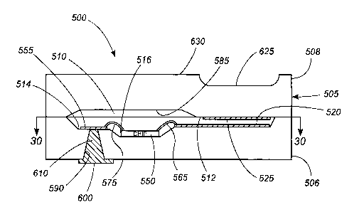
[0079] FIGS. 29 and 30 illustrate a further embodiment of a sensor 500
comprising a sensor
body 505 of fused silica, or other suitable material, as discussed above. The
sensor body 505
comprises a lower wall 506 and an upper wall 508. The lower wall 506 further
comprises a first
trench 514 and a second trench 516 formed within a portion of the first trench
514. The sensor
body 505 further defines a hermetic chamber 510. Located within the hermetic
chamber 510 on
the lower wall 506 in the area comprising the first trench 514 are electrode
520 and electrode 522.
The electrode 522 is behind and in-plane with the first electrode 520 and is
thus not visible in
Figure 29. Another electrode 525 is located within the hermetic chamber 510 on
the upper wall
508 and is positioned such that it is in parallel, spaced-apart relation with
respect to electrode 520
and electrode 522. Electrode 520, electrode 522 and electrode 525 combine to
form a gap
capacitor.
[0080] The second trench 516 in the lower wall 506 contains a silicon chip 550
bearing
electronics. Located on the opposite side of the first trench 514 from the
electrodes 520, 522, and
525 are electrode 555 and electrode 560. Electrode 560 is behind and in-plane
with the electrode
25.
CA 02652060 2008-11-12
WO 2008/066569 PCT/US2007/011612
555 and is thus not visible in Figure 29. A conductor 565 places the electrode
520 in electrical
communication with a wire bond on the chip 550. Similarly, a conductor 570
places the electrode
522 in electrical communication with a second wire bond on the chip 550. The
wire bond 570 is
behind and in-plane with the wire bond 565 and is thus not visible in Figure
29. A third
conductor 575 places the electrode 555 in electrical communication with a
third wire bond on the
chip 550. A fourth conductor 580 places the electrode 560 in electrical
communication with a
fourth wire bond on the chip 550.
[00811 A third trench 585 is provided in the upper wall 508. The upper wall
508 of the
sensor 500 acts as a deflective region 625 and is configured to be
sufficiently thin to deflect in
response to physiologically relevant pressure changes. As explained in
previous examples, the
electrode 525 is coupled to this deflective region 625 so that the distance
between the electrode
525 and the electrodes 520, 522 changes with variations in external pressure,
thereby changing
the characteristic capacitance of the capacitor.
[00821 The lower wall 506 of the sensor body 505 comprises passages 590 and
595 that
traverse the sensor body 505 and are in contact with the electrodes 555, 560.
As shown in FIGS.
29 and 30, electrical contact pads 600, 605 can be formed on the back side of
the electrodes 555,
560 and extend to the exterior of the housing, thereby providing a region on
the exterior of the
sensor 500 configured with sufficient dimensions so as to allow for a means
for connection with
external electronics. As an alternative, the passages 590, 595 can be filled
with an electrically
conductive material, with contact pads 600, 605 in electrical communication
with the electrodes
555, 560 by way of the conductive material 610. The electrode 555, the passage
590, and, if
present, the electrical contact pad 600 and any electrically conductive
material 610 filling the
passage 590 comprises a first electrical feedthrough. The electrode 560, the
passage 595, and, if
present, the electrical contact pad 605 and any electrically conductive
material 610 filling the
passage 595 comprises a second electrical feedthrough.
26.
CA 02652060 2008-11-12
WO 2008/066569 PCT/US2007/011612
[0083] The fabrication of the sensor 500 depicted in FIGS. 29 and 30 is based
on the
micromachining of two substrates that are subsequently brought into contact
and cut into
individual sensors. The fabrication of the individual sensors as well as their
final assembly is
described as follows: A lower substrate is provided. Into this lower
substrate, a first trench is
etched that is 2 mm by 5 mm and 3 micrometers deep using conventional masking
processes and
wet etching techniques, as described in earlier examples. A second trench is
then etched in a
portion of the lower substrate using the same methods as used in creation of
the first trench. In the
disclosed example, the second trench is 100 micrometers deep, 1.3 mm long, and
0.9 mm wide.
Next, the four electrodes deposited on the lower wall are formed by
conventional masking
techniques and thin film techniques as described in previous examples. The
chip is then inserted
in the recessed cavity and fixed by, e.g., a press fit, adhesive, or eutectic
bonding via additional
metallic interfaces such as a soldered preforms. After the chip is placed and
fixed to the lower
substrate, the four conductors associated with the four electrodes deposited
on the lower wall are
made via conventional techniques, e.g., with wire that is 25 micrometers in
diameter.
[0084] Next, the upper substrate is prepared. To this end, a third trench is
etched into this
wafer using the same techniques as used to create the first and second
trenches of the lower
substrate. In the disclosed embodiment, this trench is 2.5 mm long, 1.7 mm
wide, and 0.1 mm
deep. The electrode deposited on the upper wall is then created using the same
techniques
referenced in the creation of the electrodes on the lower substrate. This
electrode deposited on
the upper wall is 1.4 mm by 2 mm and made of 500 nm layer of Chrome/Gold.
[0085] Subsequent to individual fabrication of the substrates, the upper wafer
is oriented with
respect to the lower wafer such that the components are aligned as shown in
FIGS. 29 and 30.
The wafers form a temporary bond and are optionally further subjected to a 200
degrees C oven
for approximately two hours in order to increase the bond strength.
[0086] Passages 590, 595 are created through the exterior surface of the lower
substrate using
a CO2 laser as described previously. After laser ablation, the passages are
optionally subjected to
27.
CA 02652060 2008-11-12
WO 2008/066569 PCT/US2007/011612
a wet etch. The passages resulting from this process are approximately 200
micrometers at the
exterior surface and about 50 micrometers at the interior surface and the back
side of the fourth
and fifth electrodes are exposed. Next, a metal layer is deposited through a
shadow mask using a
DC sputterer. Any suitable metal may be used. In one embodiment, the metal
used is titanium
and the resulting layer is 10 micrometers thick. This titanium layer is
intended to establish
electrical communication between the interior of the hermetic chamber and the
ambient.
Furthermore, the titanium layer increases the integrity of the hermetic cavity
and provides further
corrosion resistance.
[0087] The capacitor contained within the individualized sensor made with the
above
geometry is approximately 5 picofarads. It is obvious to one skilled in the
art in light of the
present disclosure to modify the spacing between the electrodes as well as the
area of the
interposed electrodes to increase or decrease the capacitance value.
[0088] The sensor is then individualized from the two wafer stack using the
same method as
disclosed in previous embodiments.
[0089] Regarding the manufacture of the sensor, the overall size of the
resultant device can be
reduced through use of an anisotropic etching method (e.g., ICP glass etching,
ultrasonic glass
etching) instead of isotropic wet etching. If the chip utilized in the example
above is 800 by 1300
micrometers, the second trench in the lower wafer can very well be merely 810
by 1310
micrometers. Also, the capacitor area can be reduced to 700 microns by 800
microns by reducing
the gap between the electrodes. Furthermore, the thickness of the fused silica
package can also be
reduced to about 100 micrometers by reducing the thickness of the wall
surrounding the hermetic
cavity. Thus, it follows that the sensor of the present embodiment can be
reduced to final overall
dimensions of 1 mm by 2.3 mm by 0.6 mm versus the disclosed example that
results in a device
that is 2 mm by 5 mm by 0.6 mm, as shown in Figure 30. In addition, if no chip
is included in the
sensor package the sensor (such as that disclosed in Figure 1) can achieve
even smaller
28.
CA 02652060 2008-11-12
WO 2008/066569 PCT/US2007/011612
geometries. Also, as obvious to one skilled in the art, the aspect ratio
(length to width) can be
altered and achieve similar results.
[0090] In an alternative example, a piezoresistive transduction scheme can be
utilized to
measure changes in the position of the deflectable region in the pressure
cavity. One or more
piezoresistive elements translate mechanical strain into changes in electrical
resistance. The
piezoresistor is made of, e.g., polysilicon and formed on the interior of the
pressure cavity in lieu
of the electrodes in previous examples. The resistance modulation is, e.g.,
detected through a
fully active Wheatstone bridge, as is known in the art. Optimally, the
Wheatstone bridge
configuration used is one where only one leg of the bridge is fixed to the
deflectable region of the
pressure cavity. This design reduces the number of feedthroughs to two.
[0091] While the invention as been illustrated in the context of a biological
device, it will be
appreciated that the hermetic chamber herein described can be adapted to non-
biological
applications, for example, industrial applications in which a harsh
environment is encountered.
[0092] Referring now to FIGS. 31 and 32, in another aspect of this invention,
a fixture is
provided to house previously individualized sensors in alignment for
subsequent processing or
shipping. The fixture 700 includes a plurality of recesses 702, each adapted
to house a sensor, or
other suitable micro-device. The fixture can be used, e.g., to position
multiple individualized
sensors with respect to features on a mask, allowing for contact between the
mask and the
sensors, and as a shipping container. This fixture is useful for micro-devices
which are small and
not easily handled or manipulated, such as those described previously. Also,
this method will
effectively prevent contamination of device surfaces during handling and
processing.
Furthermore, this fixture enables a batch technique to define features on the
surface of individual
devices. This feature is particularly useful when deposition of metal on the
exterior of such a
device would compromise subsequent processes (e.g., coating, bonding) or would
prohibit the
creation of an operable device due to thermal or chemical considerations.
E.g., if fused silica is
used to create a sensor according to this invention and the feedthroughs
comprise Ti, then the
29.
CA 02652060 2008-11-12
WO 2008/066569 PCT/US2007/011612
fused silica cannot be cleaned with hydrofluoric acid (HF) as would normally
be done. The HF
will also etch away the Ti. With this process, the sensors may be
individualized, cleaned and
placed in this fixture, where the deposition of thick Ti pads would occur
after cleaning. The
fixture would preserve the cleanliness of the other surfaces so as to allow
for coating or
subsequent processing while one avoids exposing the Ti pads on the exterior of
the fixture to a
deleterious substance during manufacture of the device.
[0093] The accuracy of the features placed on the microfabricated device
(e.g., sensor), the
deposition method used to define additional features on the device surface,
the tolerance of the
manufacturing technique used to create the recesses in the fixture and the
tolerance of the device
itself are all factors in determining the tolerances of the final fixture.
Thus, a manufacturing
method should be chosen to make the fixture that is capable of defining
features that correspond
with allowable tolerances of the final device. The fixture can be made out of
silicon (sub-micron
tolerances), fused silica (10 micron tolerances with laser) or machined metal
(1 mil tolerances) or
any combination thereof. Also, if a first substrate with holes and a second
substrate are fixed
together to create the fixture, then the alignment and bonding method used to
create the fixture
also influences the tolerances of the accuracy of the final features placed on
the device.
[0094] A pick-and-place operation can then be utilized to insert the devices
into individual
recesses. Then, the substrate can be "capped" with a final substrate to
provide a shipping
container.
[0095] Alternatively, or before capping to create a shipping container, a
shadow mask is
provided in order to facilitate the addition of metal features to the surface
of the device. Here, the
fixture containing the devices is placed on a first platform. Then, the shadow
mask is connected
to a base wafer and the mask is aligned. Contact is made between the shadow
mask and the
fixture by alignment equipment which is well-known in the art. After contact
is made, the
shadow mask and fixture are secured by some form of mechanical fixation to
prevent any relative
movement. The machine used to apply the metal to the device is common to
microelectronics
30.
CA 02652060 2008-11-12
WO 2008/066569 PCT/US2007/011612
and utilizes physical vapor deposition (PVD) techniques. These machines are
designed to hold
wafers from at least 2 in. to about 12 in. in diameter, thus the substrates of
the present invention
can be wafers of these dimensions.
[0096] Si02 Fixture Example: To create a fixture from fused silica, two
substrates are
utilized and the dimensions of the device to be placed in the fixture are
known. A first substrate
thickness is selected such that it is less than the height of the device to be
placed in the fixture.
Then, holes are cut all the way through this first substrate using, e.g., a
C02 laser operating at a
peak wavelength of 10 microns. Then a second fused silica substrate is
provided and placed in
contact with the first substrate.
[0097] The bonding and subsequent uppermost surface of the fixture should be
uniform
enough so that the devices are maintained at a certain height above the height
of the substrate and
no part of the substrate is as tall as or taller than the device. For fused
silica, direct bonding (use
Van der Waals forces); adhesives; highly localized heat (e.g., a C02 laser),
or a mechanical
clamp (in conjunction with the mask) could be used alone or in combination to
bond or otherwise
fix the two substrates together.
[0098] Si Fixture Example: For a silicon fixture only one substrate is
necessary. The
recesses are created by known techniques using inductively-coupled plasma.
This method
provides a highly reliable and accurate method to create the fixture. Again,
the recess dimensions
dictate the initial substrate thickness and the dimensions of the recesses
created therein.
[0099] Alternatively, a Si fixture could be constructed with the two wafer
process described
above the in the Si02 fixture and bonded with conventional Si bonding methods.
All
manufacturing techniques used in the construction of this fixture are known to
those skilled in the
art.
[00100] Metal Machining Example: Metal machining techniques can also be
utilized to create
the fixture of the present invention. Such techniques are well-known in the
art.
31.
CA 02652060 2008-11-12
WO 2008/066569 PCT/US2007/011612
[00101] Finally, if two substrates are used to construct the fixture
combinations such as
silicon-fused silica and fused silica-metal can be utilized. Methods to bond
these dissimilar
substrates are well known in the art.
[00102] Specific embodiments have been described herein, by way of example and
for clarity
of understanding, and variations and modifications to the present invention
may be possible given
the disclosure above. Hence the scope of the present invention is limited
solely by the appended
claims.
32.