Note: Descriptions are shown in the official language in which they were submitted.
CA 02652695 2012-01-30
74769-2223
FAST IN-PHASE AND QUADRATURE IMBALANCE CALIBRATION
BACKGROUND
FIELD OF THE INVENTION
[002] Embodiments of the invention relate to the field of communication,
and
more specifically, to in-phase and quadrature imbalance calibration.
DESCRIPTION OF RELATED ART
[003] Radio frequency (RF) receivers or transmitters employing direct
conversion architectures generate in-phase and quadrature (I-Q) analog
signals.
These signals usually have distortions which limit demodulator or modulator
performance. These distortions, called quadrature errors, are caused by the
gain and
phase imbalances between the I-Q signal components. Imbalance in I-Q signals
may
induce an image frequency and direct current (DC) offset which interfere with
the
demodulation or modulation process. To correct the I-Q imbalance, it is
necessary to
calibrate the communication subsystem. Existing calibration methods typically
utilize
iterative approaches. These techniques correct the phase error, then the gain
error,
repeatedly in iterative sweeps.
[004] Existing calibration techniques have a number of disadvantages.
First,
the iterative approach requires multiple processing passes, resulting in long
processing time. This long processing time may cause a communication receiver
or
transmitter to be out-of-service. For communications services requiring
constant bit
rates, such as telephony or real-time video, the out-of-service interruption
may cause
undesirable performance. Second, the iterative nature of the technique is not
accurate and achieves poor results, leading to degraded performance.
SUMMARY OF THE INVENTION
According to one aspect of the present invention, there is provided a
method comprising: storing N digitized samples 1(n) and Q(n) representing in-
phase
1
CA 02652695 2012-01-30
= 74769-2223
and quadrature (I-Q) components, respectively, of a down-converted signal from
a
receiver, the I-Q components being generated from a quadrature demodulator or
modulator having I-Q imbalance; and computing phase and gain adjustment
constants from the N digitized samples to compensate for the I-Q imbalance
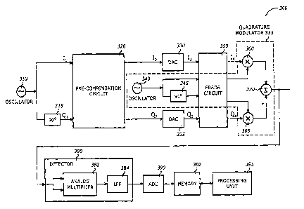
using a
closed form solution.
According to another aspect of the present invention, there is provided
a method comprising: injecting a first signal at a first frequency to a
transmitter having
a quadrature modulator with an in-phase and quadrature (I-Q) imbalance, the
quadrature modulator having a carrier frequency, the transmitter generating a
transmitter signal; detecting the transmitter signal to generate a composite
signal
having the first signal and a second signal at a second frequency twice the
first
frequency; digitizing the composite signal; and computing 1-0 direct current
(DC)
offset, phase, and gain corrections, VIc, VQc, Acik, and AGc, from the
digitized
composite signal to correct the I-Q imbalance using a closed form solution.
According to still another aspect of the present invention, there is
provided an apparatus comprising: a first adder to add a first product to a
second
product to produce a first in-phase (1) component in a communication path of a
communication device, the communication path having a quadrature demodulator
or
modulator to translate frequency of a signal, the quadrature demodulator or
modulator having I and quadrature (Q) imbalance; a second adder to add a third
product to a fourth product to produce a first quadrature (Q) component in the
communication path; first and second multipliers coupled to the first adder to
multiply
second I and Q components in the communication path with first and second
adjustment constants, respectively, to produce the first and second products,
respectively; and third and fourth multipliers coupled to the second adder to
multiply
the second land Q components in the communication path with third and fourth
adjustment constants, respectively, to produce the third and fourth products,
respectively; wherein the first, second, third, and fourth adjustment
constants are
computed using a closed form solution to compensate for the I-Q imbalance.
la
CA 02652695 2012-01-30
= 74769-2223
According to yet another aspect of the present invention, there is
provided an apparatus comprising: a quadrature modulator circuit in a
transmitter to
generate a transmitter signal, the quadrature modulator circuit having in-
phase and
quadrature (l-Q) imbalance; an error circuit coupled to the quadrature
modulator
circuit and l-Q digital-to-analog converters (DACs) to model the l-Q
imbalance; and a
pre-compensation circuit coupled to modulator in-phase and quadrature (l-Q)
components of a modulator of the transmitter to generate pre-compensated 1-0
components to the l-Q DACs, respectively, using compensation constants to
compensate for the I-0 imbalance, the compensation constants being computed
using a closed-form solution in calibration procedure.
According to a further aspect of the present invention, there is provided
an article of manufacture comprising: a machine-accessible storage medium
including information that, when accessed by a machine, cause the machine to
perform operations comprising: storing N digitized samples 1(n) and Q(n)
representing
in-phase and quadrature (l-Q) components, respectively, of a down-converted
signal
from a receiver, the l-Q components being generated from a quadrature
demodulator
or modulator having l-Q imbalance; and computing phase and gain adjustment
constants from the N digitized samples to compensate for the l-Q imbalance
using a
closed form solution.
According to yet a further aspect of the present invention, there is
provided an article of manufacture comprising: a machine-accessible storage
medium
including information that, when accessed by a machine, cause the machine to
perform operations comprising: injecting a first signal at a first frequency
to a
transmitter having a quadrature modulator with an in-phase and quadrature (1-
0)
imbalance, the quadrature modulator having a carrier frequency, the
transmitter
generating a transmitter signal; detecting the transmitter signal to generate
a
composite signal having the first signal and a second signal at a second
frequency
twice the first frequency; digitizing the composite signal; and computing l-Q
direct
current (DC) offset, phase, and gain corrections, Vic, VQc, Mk, and AGO, from
the
lb
CA 02652695 2012-01-30
74769-2223
digitized composite signal to correct the I-Q imbalance using a closed form
solution.
According to still a further aspect of the present invention, there is
provided a system comprising: a quadrature demodulator to down-convert a radio
frequency (RF) signal received at a receiver subsystem, the quadrature
demodulator
providing analog in-phase and quadrature (I-0) components that have l-Q
imbalance,
the quadrature demodulator having mixers; analog-to-digital converters (ADCs)
coupled to the quadrature demodulator to convert the I-Q components into
digital I-0
components; and a compensator coupled to the ADCs to compensate the I-0
imbalance, the compensator comprising: a first adder to add a first product to
a
second product to produce an output I component, a second adder to add a third
product to a fourth product to produce an output Q component, first and second
multipliers coupled to the first adder to multiply the digital I and Q
components with
first and second adjustment constants, respectively, to produce the first and
second
products, respectively, and third and fourth multipliers coupled to the second
adder to
multiply the digital I and Q components with third and fourth adjustment
constants,
respectively, to produce the third and fourth products, respectively; wherein
the first,
second, third, and fourth adjustment constants are computed using a closed
form
solution to compensate for the I-Q imbalance.
According to another aspect of the present invention, there is provided
a system comprising: a quadrature modulator to up-convert analog in-phase and
quadrature (I-Q) components of a base-band signal to a transmitting signal,
the
quadrature modulator having mixers that generate I-0 imbalance; digital-to-
analog
converters (DACs) coupled to the quadrature modulator to convert pre-
compensated
I-Q components to the analog I-Q components; and a compensator coupled to the
DACs to compensate for the l-Q imbalance from modulator I-Q components, the
compensator comprising: a first adder to add a first product to a second
product to
produce the pre-compensated I component, a second adder to add a third product
to
lc
CA 02652695 2012-01-30
74769-2223
a fourth product to produce the pre-compensated Q component, first and second
multipliers coupled to the first adder to multiply the modulator I and Q
components
with first and second adjustment constants, respectively, to produce the first
and
second products, respectively, and third and fourth multipliers coupled to the
second
adder to multiply the modulator I and Q components with third and fourth
adjustment
constants, respectively, to produce the third and fourth products,
respectively;
wherein the first, second, third, and fourth adjustment constants are computed
using
a closed form solution to compensate for the I-Q imbalance.
id
CA 02652695 2008-11-18
WO 2007/146090 PCT/US2007/013459
BRIEF DESCRIPTION OF THE DRAWINGS
[005] Embodiments of the invention may best be understood by referring to the
following
description and accompanying drawings that are used to illustrate embodiments
of the
invention. In the drawings:
[006] Figure 1A is a diagram illustrating a receiver subsystem according to
one
embodiment of the invention.
[007] Figure 1B is a diagram illustrating a compensator for the receiver
subsystem
according to one embodiment of the invention.
[008] Figure 2A is a diagram illustrating a transmitter subsystem for
calibration using a
calibrated reference receiver according to one embodiment of the invention.
[009] Figure 2B is a diagram illustrating a compensator for the transmitter
subsystem
according to one embodiment of the invention.
[010] Figure 3 is a diagram illustrating a transmitter subsystem for
calibration without
using a calibrated reference receiver according to one embodiment of the
invention.
[011] Figure 4 is a diagram illustrating a pre-compensation circuit according
to one
embodiment of the invention.
=
[012] Figure 5 is a diagram illustrating an error circuit according to one
embodiment of the
invention.
[013] Figure 6 is a flowchart illustrating a process to perform calibration
according to one
embodiment of the invention.
[014] Figure 7 is a flowchart illustrating.a process to compute the phase and
gain
adjustment constants according to one embodiment of the invention.
[015] Figure 8A is a flowchart illustrating a process to compute I-Q average
power and I-
Q correlation according to one embodiment of the invention.
[016] Figure 8B is a flowchart illustrating a process to estimate gain and
phase differences
according to one embodiment of the invention.
2
CA 02652695 2008-11-18
WO 2007/146090 PCT/US2007/013459
[0171 Figure 8C is a flowchart illustrating a process to compute a matrix A of
the
adjustment constants according to one embodiment of the invention.
[018] Figure 9 is a flowchart illustrating a process to calibrate a
transmitter without using a
calibrated reference receiver according to one embodiment of the invention.
[019] Figure 10A is a flowchart illustrating a process to detect the
transmitter signal
according to one embodiment of the invention.
[020] Figure 10B is a flowchart illustrating a process to compute the I-(2 DC
offset, phase,
and gain corrections according to one embodiment of the invention.
[021] Figure 11 is a diagram illustrating a processing unit according to one
embodiment of
the invention.
3
CA 02652695 2008-11-18
WO 2007/146090 PCT/US2007/013459
DESCRIPTION
[022] An embodiment of the present invention includes a technique to calibrate
receiver
and transmitter in a communication system. N digitized samples I(n) and Q(n)
are stored.
The N digitized samples represent in-phase and quadrature (I-Q) components,
respectively,
of a down-converted signal from a receiver. The I-Q components are generated
from a
quadrature modulator or demodulator having I-Q imbalance. Phase and gain
adjustment
constants are computed from the N digitized samples to compensate for the I-Q
imbalance
using a closed form solution.
[023] Another embodiment of the present invention includes a technique to
calibrate a
transceiver in a communication system without using a calibrated reference
receiver. A first
test signal at a first frequency is injected to a transmitter having a
quadrature modulator
with I-Q imbalance. The quadrature modulator has a carrier frequency. The
transmitter
generates a transmitter signal. The transmitter signal is detected to generate
a composite
signal having the first test signal and a second test signal at a second
frequency twice the
first frequency. The composite signal is digitized. I-Q direct current (DC)
offset, phase,
and gain corrections are computed from the digitized composite signal to
correct the I-Q
imbalance using a closed form solution.
= [024] In the following description, numerous specific details are set
forth. However, it is
understood that embodiments of the invention may be practiced without these
specific
details. In other instances, well-known circuits, structures, and techniques
have not been
shown in order not to obscure the understanding of this description.
[025] One embodiment of the invention may be described as a process which is
usually
depicted as a flowchart, a flow diagram, a structure diagram, or a block
diagram. Although
a flowchart may describe the operations as a sequential process, many of the
operations can
be performed in parallel or concurrently. In addition, the order of the
operations may be re-
arranged. A process is terminated when its operations are completed. A process
may
correspond to a method, a program, a procedure, a method of manufacturing or
fabrication,
etc.
[026] Embodiments of the invention include a technique to calibrate a receiver
or a
transmitter in a communication system to compensate for I-Q imbalances in the
quadrature
demodulator or modulator circuit. The calibration is performed in the digital
domain using
a closed-form solution to provide fast calibration. The closed-form solution
includes
application of formulas or equations to compute the adjustment constants or
the imbalance
4
CA 02652695 2008-11-18
WO 2007/146090 PCT/US2007/013459
corrections. After calibration, the adjustment constants or imbalance
corrections may be
applied in the compensator circuit to compensate for the I-Q imbalance. The
compensation
is performed in the digital domain.
[027] In one embodiment, the technique is used to calibrate a receiver. An
input signal is
injected into the input of the RF receiver. The signal goes through the mixing
process in the
quadrature demodulator circuit to be down-converted to base-band signal. The
base-band
signal is then converted to digital samples. The digitized samples are stored
in memory to
be processed by a processing unit. The processing unit computes the adjustment
constants
from the stored digitized samples using a closed-form solution. The
computation of the
adjustment constants therefore takes place in one single pass, involving
direct calculations
of the constants using formulas. Accordingly, the calibration is fast,
efficient, and accurate.
[028J The same procedure may be used to calibrate a transmitter. In this
scheme, a
calibrated reference receiver is needed to provide the receiver path for the
signal. A
reference test signal is passed through the transmitter quadrature modulator
that has the
imbalance that needs to be compensated. The generated transmitted signal is
looped back to
the calibrated reference receiver. Since the calibrated reference receiver
introduces no
distortions, the distortions in the received signal are caused by the
transmitter quadrature
modulator. The same procedure to compute the phase and gain adjustment
constants for the
receiver calibration is used.
[029] After the adjustment constants are computed, they may be applied to the
receiver or
the transmitter to compensate for the I-Q imbalance in the quadrature
demodulator or
modulator. For a receiver, these constants are applied after the down-
conversion by the RF
quadrature demodulator on the I-Q signals. For a transmitter, these constants
are applied
before the up-conversion by the RF quadrature modulator on the I-Q signals to
pre-
compensate for the I-Q imbalance. In both cases, the compensation is performed
in the
digital domain.
[030] An alternative method to calibrate a transmitter without using a
calibrated reference
receiver. This technique utilizes a transmitter Power detector built into the
RF transceiver
circuit. A first test signal is generated to go through the quadrature
modulator in the
transmitter. The transmitter signal passes through a detector. The detector
includes a
squarer and a low pass filter. The low pass filter removes the carrier
frequency of the
quadrature modulator. The detector generates a composite signal having the
first signal and
a second signal at a second frequency twice the first frequency. The composite
signal is
=
CA 02652695 2008-11-18
WO 2007/146090 PCT/US2007/013459
then digitized by an analog and digital converter. The digitized samples of
the composite
signal are stored. A processing unit computes I-Q DC offset, phase, and gain
corrections
from the digitized composite signal using a closed form solution. The I-Q DC
offset, phase,
and gain corrections are used to pre-compensate the I-Q balance in a pre-
compensation
circuit before the quadrature modulator circuit. The computation of the
corrections
therefore takes place in one single pass, involving direct calculations of the
corrections
using formulas. Accordingly, the calibration is fast, efficient, and accurate.
[031] Figure lA is a diagram illustrating a receiver subsystem 100 according
to one
embodiment of the invention. The receiver subsystem 100 includes a bandpass
filter (BPF)
110, a low-noise amplifier (LNA) 115, a quadrature demodulator circuit 120, I-
Q analog-to-
digital converters 150 and 155, an 1-Q imbalance compensator 160, a digital
demodulator
170, a memory 180, and a processing unit 190. The receiver subsystem 100 may
include
more or less than the above components.
[0321 The input signal is received from an RF antenna. The BPF 110 removes
unwanted
frequencies from the frequency band of interest. The LNA 115 amplifies the
filtered signal
with proper gain.
[033] The quadrature demodulator 120 down converts the received signal to base-
band
signal. The quadrature demodulator 120 includes a local oscillator 125, a
splitter 127, two
mixers 130 and 135, and two buffers 140 and 145. The local oscillator 125
generates a
carrier waveform having a carrier frequency. The splitter 127 splits the
carrier waveform
. into two waveforms that are phase shifted by 90 . The mixers 130 and 135
mix, or
multiply, the received signal with the phase shifted signals to provide two
channels: the in-
phase (I) channel and the quadrature (Q) channel. The two buffers 140 and 145
buffer the
resulting I-Q components of the quadrature demodulated signal. The quadrature
demodulator 120 may have I-Q imbalance that cause signal distortions.
[034] The I-Q ADCs 150 and 155 convert the respective I-Q components from the
quadrature demodulator 120 into digital data. The I-Q compensator 160
compensates the I-
Q imbalance in the quadrature demodulator 120 to provide corrected
components. The
I-Q compensator 160 uses the adjustment constants as computed by the
processing unit 190
to perform the compensation. During calibration, the I-Q compensator 160 may
be in
calibration mode that passes the digitized I-Q components without change.
After
calibration, the I-Q compensator 160 may be loaded with the adjustment
constants and
6
CA 02652695 2008-11-18
WO 2007/146090 PCT/US2007/013459
activated to perform the compensation function. The digital demodulator 170
applies
digital demodulation to the corrected I-Q components according to the receiver
functions.
[035] The memory 180 stores N digitized I-Q samples for processing. It may be
any
storage device (e.g., fast static random access memory) that can store the
digitized I-Q
samples at the real-time rate. The size of the memory is selected according to
the desired
number of digitized samples to be stored.
[036] The processing unit 190 includes a programmable processor that executes
programs =
or instructions to compute the adjustment constants to compensate for the I-Q
imbalance.
The processing unit 190 provides the adjustment constants to the I-Q
compensator 160.
[037] Figure 1B is a diagram illustrating the compensator 160 for the receiver
subsystem
in Figure 1A according to one embodiment of the invention. The compensator 160
includes
the adjustment constants all, a12, a21, and a22, 10, 15, 20, and 25, two
adders 162 and 163,
and four multipliers 164, 165, 166, and 167.
[038] The adjustment constants all, a12, a21, and a22 10, 15, 20, and 25 are
the gain and
phase adjustment constants or corrections to compensate for the I-Q imbalance
as computed
in a closed-form solution by the processing unit 190 during a calibration
procedure. They
may be stored in storage elements such as registers, buffer memory, or any
other storage
elements including hardwired data. They are components of the matrix A as
computed by
the processing unit 190 described in the process 730 shown in Figure 8C.
[039] The adder 162 adds a first product P1 to a second product P2 to produce
the I
component in the communication path of the receiver subsystem 100. As
described above,
the communication path has a quadrature demodulator to translate frequency of
the received
signal. The quadrature demodulator has I-Q imbalance or distortion that may be
compensated or corrected by the gain and phase adjustment constants ail, a12,
a21, and a22.
The adder 163 adds a third product P3 to a fourth product P4 to produce the Q
component in
the communication path.
[040] The multipliers 164 and 166 multiply the input I' and Q' components in
the
communication path with the adjustment constants an and a12, 10 and 15,
respectively, to
produce the first and second products P1 and Py, respectively, to the adder
162. The
multipliers 165 and 167 multiply the input Q' and I' components in the
communication path
with the adjustment constants a22 and a21, 20 and 25, respectively, to produce
the third and
fourth products P3 and 134, respectively.
7
CA 02652695 2008-11-18
WO 2007/146090 PCT/US2007/013459
=
[041] Figure 2A is a diagram illustrating a transmitter subsystem 200 for
calibration using
a calibrated reference receiver according to one embodiment of the invention.
The
transmitter subsystem 200 includes a digital modulator 210, an I-Q compensator
220, I-Q
digital-to-analog converters (DACs) 230 and 235, I-Q low pass filters (LPFs)
240 and 245,
a quadrature modulator 250, a power amplifier (PA) 285, a calibrated reference
receiver
290, a memory 292, and a processing unit 295. The transmitter subsystem 200
may include
more or less than the above components. During calibration, the calibrated
reference
receiver 290, the memory 292, and the processing unit 295 are used to compute
the
adjustment constants used in the I-Q compensator 220. After the adjustment
constants are
computed, the processing unit 295 loads these constants into the compensator
220. The
calibrated reference receiver 290, the memory 292, and the processing unit 295
may then be
removed.
[042] The digital modulator 210 performs digital modulation according to the
transmitter
function. This may include various encoding functions such as error coding,
etc. The I-Q
compensator 220 applies the adjustment constants or imbalance corrections to
pre-
compensate for the I-Q imbalance or distortions in the quadrature modulator
250. The I-Q
DACs 230 and 235 convert the I-Q digital data to analog base-band signals. The
LPFs 240
and 245 low pass filter the analog base-band signals on the respective I-Q
channels to
remove unwanted frequencies.
[043] The quadrature modulator 250 up-converts the base-band signals to the
desired
frequency. The quadrature modulator 250 includes a local oscillator 255, a
splitter 260,
two mixers 270 and 275, and a combiner 280. The local oscillator 255 generates
a carrier
waveform having a carrier frequency. The splitter 260 splits the carrier
waveform into two
waveforms that are phase shifted by 90 . The mixers 270 and 275 mix, or
multiply, the
base-band signals with the phase shifted signals to provide I-Q components of
the RF signal
to be transmitted. The quadrature modulator 250 may have I-Q imbalance that
cause signal
distortions. The combiner 280 combines, or adds, the I-Q components of the RF
signal into
a composite RF output signal.
. [044] The PA 285 amplifies the composite RF signal for transmission to an RF
antenna.
The calibrated reference receiver 290 is a receiver subsystem that has been
calibrated to
compensate for I-Q imbalance in its quadrature demodulator. It is similar to
the receiver
subsystem 100. The memory 292 and the processing unit 295 are similar to the
memory
180 and the processing unit 190, respectively, shown in Figure 1A. The memory
292 stores
=8
CA 02652695 2008-11-18
WO 2007/146090 PCT/US2007/013459
=
digitized samples of the received signal. The processing unit 295 computes the
adjustment
constants to be used in the compensator 220.
[045] Figure 2B is a diagram illustrating the compensator 220 for the
transmitter
subsystem according to one embodiment of the invention. The compensator 220
includes
the adjustment constants aii, a12, a21, and a22, 10, 15, 20, and 25, two
adders 222 and 223,
and four multipliers 224, 225, 226, and 227.
[046] The adjustment constants a11, at2, a21, and a22 10, 15, 20, and 25 are
the gain and
phase adjustment constants or corrections to compensate for the
imbalance as computed
in a closed-form solution by the processing unit 295 during a calibration
procedure. These
are similar to the constants shown in Figure 1B. They may be stored in storage
elements
such as registers, buffer memory, or any other storage elements including
hardwired data.
They are components of the matrix A as computed by the processing unit 295 as
described
in the process 730 shown in Figure 8C.
[047] The adder 222 adds a first product P1 to a second product P2 to produce
the I'
component in the communication path of the transmitter subsystem 200. As
described
above, the communication path has a quadrature modulator to translate
frequency of the
base-band signal. The quadrature modulator has imbalance or distortion that
may be
pre-compensated or corrected by the gain and phase adjustment constants all,
ai2, a2i, and
a22. The adder 223 adds a third product P3 to a fourth product P4 to produce
the Q'
component in the communication path.
[048] The multipliers 224 and 226 multiply the input I and Q components in the
communication path with the adjustment constants all and a12, 10 and 15,
respectively, to
produce the first and second products P1 and P2, respectively, to the adder
222. The
multipliers 225 and 227 multiply the input Q and I components in the
communication path
with the adjustment constants a22 and a21, 20 and 25, respectively, to produce
the third and
fourth products P3 and P4, respectively.
[049] The calibration of the transmitter subsystem 200 is performed using the
calibrated
reference receiver 290. When such receiver is not available, an alternate
calibration
technique may be employed. This technique may be illustrated in Figure 3.
[050] Figure 3 is a diagram illustrating a transmitter subsystem 300 for
calibration without
using a calibrated reference receiver according to one embodiment of the
invention. The
transmitter subsystem 300 includes a signal generator 310, a phase shifter
315, a pre-
. 9
CA 02652695 2008-11-18
WO 2007/146090 PCT/US2007/013459
compensation circuit 320, two I-Q DACs 330 and 335, an error circuit 350, a
quadrature
modulator 355, a detector 380, an analog-to-digital converter 390, a memory
392, and a
processing unit 395. The transmitter subsystem 300 may include more or less
than the
above components.
[051] The signal generator 310 generates a test signal at a pre-determined
frequency. The
test signal becomes the I component, i.e., II in the communication path. The
phase shifter
315 phase shifts the test signal 90 to provide the Q component, e.g., Qi. The
signal
generator 310 and the phase shifter 315 may be used to emulate a digital
modulator
normally used in a transmitter. The signal generator 310 therefore may be
implemented as a
digital signal generator that generates digital data. The test signal may be a
single-tone
signal that has a single frequency. In other words, it may be generated as a
sinusoidal
waveform at a pre-determined frequency.
[052] The pre-compensation circuit 320 receives the I-Q components II and Q1
of the
modulator as emulated by the signal generator 310 and the phase shifter 315 to
generate pre-
compensated I-Q components 12 and Q2 to the I-Q DACs 330 and 335,
respectively. The
pre-compensation circuit 320 uses compensation constants to compensate for the
I-Q
imbalance in the quadrature modulator 355. The compensation constants are
computed
using a closed-form solution in a calibration procedure.
[053] The I-Q DAC2 330 and 335 convert the respective I-Q digital data 12 and
Q2 from
the pre-compensation circuit 320 to analog I-Q base-band signals 13 and Q3,
respectively.
The error circuit 350 models the I-Q imbalance in terms of DC offset, gain
error, and phase
error.
[054] The quadrature modulator 355 up-converts the base-band signals to the
desired
frequency. The quadrature modulator 355 includes a local oscillator 340, a
phase shifter
345, two mixers 360 and 365, and a combiner 370. The local oscillator 340
generates a
carrier waveform having a carrier frequency. The original carrier waveform
corresponds to
the I component. The phase shifter 345 phase shifts the carrier waveform by 90
to
correspond to the Q component. The mixers 360 and 365 mix, or multiply, the
base-band
signals as passed by the error circuit 350 with the original and the phase
shifted signals to
provide I-Q components of the RF signal to be transmitted. The quadrature
modulator 355
may have I-Q imbalance that cause signal distortions. The combiner 370
combines, or
= adds, the I-Q components of the RF signal into a transmitter signal.
CA 02652695 2008-11-18
WO 2007/146090
PCT/US2007/013459
[0551 During calibration, the transmitter signal from the quadrature modulator
355 is fed
to the detector 380. The detector 380 generates a composite signal having the
first signal as
the test signal first and second frequencies from the transmitter signal, the
second frequency
being twice the first frequency. The detector 380 includes an analog
multiplier 382 and a
low-pass filter (LPF) 384. The analog multiplier 382 multiplies the
transmitter signal to
itself, or squares the transmitter. If the transmitter signal contains the
test signal which is a
single-tone sinusoidal signal, the squaring introduces an additional second
test signal having
a second frequency which is twice the frequency of the test signal. The LPF
384 has a
corner frequency at approximately above the second frequency. Since the first
frequency is
much less than the carrier frequency, the second frequency is also much less
than the carrier
frequency. The LPF 384 therefore removes the carrier frequency while passing
the first and
second signals. The magnitudes and phases of the first and second signals
provide a
relationship with the DC offset, phase and gain en-ors due to the I-Q
imbalance. The ADC
390 converts the analog signal from the detector to digital data to provide
digitized samples
of the composite signal. The digitized samples are used to compute the
compensation
constants.
[056] The memory 392 and the processing unit 395 are similar to the memory 292
and the
processing unit 295, respectively, shown in Figure 2A. The memory 392 stores
digitized
samples of the composite signal. The processing unit 395 computes the
compensation
constants to be used in the pre-compensator 320.
[057] Figure 4 is a diagram illustrating the pre-compensation circuit 320
shown in Figure
3 according to one embodiment of the invention. The includes an I-Q gain
imbalance
circuit 410, an I-Q phase imbalance circuit 440, and a DC offset circuit 470.
[058] The I-Q gain imbalance circuit 410 generates I-Q gain pre-compensated
components. It includes gain
multipliers 420 and 425 to multiply the modulator I-Q
components Ili and Qi with I-Q gain compensation constants 430 and 435 to
produce the IQ
gain pre-compensated components. The I-Q gain compensation constants 430 and
435 are
GAIN/2 and ¨GAIN/2, respectively. The value of GAIN is the AGc as shown in
Figure 10B
and computed as described in the associated description.
[059] The I-Q phase imbalance circuit 440 generates I-Q gain and phase pre-
compensated
components from the I-Q gain pre-compensated components. It includes
multipliers 442,
446, 452, and 456, and two adders 460 and 465.
11
=
CA 02652695 2008-11-18
WO 2007/146090 PCT/US2007/013459
[060] The multipliers 442 and 456 multiply the I-Q gain pre-compensated
components
with I-Q phase compensation constants 444 and 464, respectively, to produce
first and
second products, respectively. The I-Q phase compensation constants 444 and
464 are
cos and sin , respectively. The value of the phase 0 is the AA as shown in
Figure 10B and
computed as described in the associated description.
[061] The multipliers 452 and 446 multiply the Q-I components with the Q-I
phase
compensation constants 454 and 462, respectively, to produce the third and
fourth products,
respectively. The Q-I phase compensation constants 454 and 462 are cosi) and
sine,
respectively. The value of the phase 0 is the A0c as shown in Figure 10B and
computed as
described in the associated description.
[062] The adder 460 adds the first product to the second product to produce
the I gain and
phase pre-compensated component. The adder 465 adds the third product to the
fourth
product to produce the Q gain and phase pre-compensated component.
[063] The DC offset circuit 470 generated the imbalance pre-compensated I-Q
components. It includes I-Q DC offset adders 480 and 490 to add the I-Q gain
and phase
pre-compensated components to I-Q DC offset compensation constants 485 and
495,
respectively, to produce the pre-compensated I-Q components. The I-Q DC offset
compensation constants 485 and 495 are VI and VQ, respectively. The VI and VQ
c are
the VL and VQ, respectively, shown in Figure 10B and computed as described in
the
associated description.
[064] Figure 5 is a diagram illustrating the error circuit 350 shown in Figure
3 according
to one embodiment of the invention. The error circuit 340 includes two adders
510 and
520, two multipliers 530 and 540, and two I-Q delay elements 550 and 560.
[065] The adders subtract I-Q DC offset compensation constants 515 and 525
from
corresponding outputs of the I-Q DACs 330 and 335 to generates first and
second
differences, respectively. The I-Q DC offset compensation constants 515 and
525 are VI
and VQ, respectively.
[066] The multipliers 530 and 540 multiply the first and second differences
with negatives
of I-Q gain compensation constants 535 and 545, respectively, to produce I-Q
inputs 14 and
Q4 to the mixer circuit in the quadrature modulator 355. The I-Q gain
compensation
constants 535 and 545 are GAIN/2 and ¨GAIN/2, respectively. The I-Q delay
elements 550
12
CA 02652695 2008-11-18
WO 2007/146090 PCT/US2007/013459
and 560 provide I-Q phase errors to the I-Q carrier wave components from the
oscillator
340.
[067] Figure 6 is a flowchart illustrating a process 600 to perform
calibration according to
one embodiment of the invention.
[068] Upon START, the process 600 determines if the calibration is for a
receiver or a
transmitter. If the calibration is for a receiver, the process 600 injects a
single un-modulated
signal into the receiver (Block 610). The receiver has a quadrature
demodulator to down
convert the signal to base-band signal. The quadrature demodulator has the I-Q
imbalance
that may need to be compensated or adjusted. Next,'the process 600 stores N
digitized
samples I(n) and Q(n), where n is the sample index, representing the I-Q
components,
respectively, of the down-converted signal from the receiver (Block 620). The
I-Q
components are generated from the quadrature demodulator.
[069] Then, the process 600 computes phase and gain adjustment constants from
the N
digitized samples to compensate for the I-Q imbalance using a closed form
solution (Block
630). The process 630 is explained in Figure 7. The process 600 is then
terminated.
[070] If the calibration is for a transmitter, the process 600 generates a
signal from a
modulator in the transmitter (Block 640). The transmitter has the quadrature
modulator on
a transmitter path with the I-Q imbalance. Next, the process 600 loops the
signal back into
a receiver path having a calibrated reference receiver (Block 650). The
calibrated reference
receiver has a receiver mixer to down convert the signal to base-band signal.
The receiver
mixer has been calibrated such that it does not have I-Q imbalance. The I-Q
imbalance
embedded in the signal, therefore, is from the transmitter that is being
calibrated. The
process 600 then proceeds to block 620 to compute the adjustment constants for
the
transmitter using the closed-form solution in the same manner as the solution
for receiver
calibration except that the=adjustment constants are now used for the
transmitter.
[071] Figure 7 is a flowchart illustrating the process 630 shown in Figure 6
to compute
phase and gain adjustment constants according to one embodiment of the
invention.
[072] Upon START, the process 630 computes the in-phase average power PI; g ,
the
quadrature average power P , and the I-Q correlation RIQ from the N digitized
samples
1(n) and Q(n) (Block 710). Next, the process 630 estimates the gain difference
Ag and the
phase difference AO using the in-phase average power P1,, , the quadrature
average power
13
CA 02652695 2008-11-18
WO 2007/146090 PCT/US2007/013459
, and the I-Q correlation R,0 (Block 720). Then, the process 630 computes a
matrix
A=
[all ai2] .
using the gain difference Ag and the phase difference AO (Block 730). The
a21 a22
matrix A has components all, a12, a21, and a22 being the phase and gain
adjustment
constants. The process 630 is then terminated.
[073] Figure 8A is a flowchart illustrating the process 710 shown in Figure 7
to compute
the I-Q average powers and the I-Q correlation according to one embodiment of
the
invention.
[074] Upon START, the process 710 computes the iri-phase average power P,g
(Block
810), the quadrature average power PQ,avg (Block 820), and the I-Q correlation
Rig (Block
830) according to the following equations:
N-I
= ¨El (n)2
(1)
N-1
(2)
g N
N-1
RiQ = ¨EI (n)Q(n) (3)
N n=O
[075] The process 710 is then terminated.
[076] Figure 8B is a flowchart illustrating the process 720 to estimate gain
and phase
differences according to one embodiment of the invention.
[077] Upon START, the process 720 estimates the gain difference Ag as follows:
Ag = P ¨ P 1,avg Q,avg
where Payg = PI ,avg +2 PQ,avg
(4)
2P
[078] The derivation of equation (4) is given later in the following. Next,
the process 720
estimates the phase difference AO as follows:
R,,,
A0 = (5)
avg
[079] The derivation of equation (5) is given later in the following. The
process 720 is
then terminated.
14
CA 02652695 2008-11-18
WO 2007/146090 PCT/US2007/013459
=
[080] Figure 8C is a flowchart illustrating the process 730 shown in Figure 7
to compute a
matrix A of the adjustment constants according to one embodiment of the
invention.
[081] Upon START, the process 730 computes the gain matrix G as follows using
the gain
difference Ag as computed in equation (4).
Ag
0
G= 2 (6)
Ag 1
0
2
[082] Next, the process 730 computes the phase matrix P as follows using the
phase
difference A0 computed in equation (5).
cos(-A
2)2
P =
sift ¨14AI cost -- -A
2 2
[083] Then, the process 730 computes the product matrix M by multiplying
matrices G
and P as follows:
M = GP (8)
[084] Next, the process 730 computes matrix A as the inverse of the product
matrix M
computed in equation (8) as follows:
A=M'(9)
[085] The matrix A = [ail ail thus contains the components all, a12, a21, and
a22 which
azi an
are the phase and gain adjustment constants or imbalance corrections to be
used in the
receiver compensator 160 (Figure 1A) or transmitter compensator 220 (Figure
2A)
[086] The process 730 may also optionally update the matrix A by repeating the
above
computation and updating matrix A as follows:
B(n) = A.B(n-1) (10)
where B(0) = I, I is .the identity matrix.
=
[087] The process 730 is then terminated.
CA 02652695 2008-11-18
WO 2007/146090
PCT/US2007/013459
[088] Equations (4) and (5) provide expressions for the computations of the
phase and
gain adjustments constants. These expressions may be derived in the following.
[089] The I-Q imbalance is modeled using the following equation
[ = (1+-4 jcos(--q2A (1+---1)sin(¨"
2 2 A2 2) [I
Q' (1 -.C) sin (-'Lb-) (1 - A-`5-) cos (--C2A Q
2 2 2 2
Ag (A0 ) sin (AO (11)
1+- 0 cos
2 2 2 ) [/ =
0 1 sin (--- -A ) cos PA )
2 _ 2 2
Derivation of the gain adjustment constant Ag as shown in equation (4).
[090] Assuming AO= 0, IQ imbalance is as follows,
(l+Ag)cos(6,0) ii+ Ag )sin(A0)
2) 2)L2 j 2) [I
Q' ri_ Ag )sin A0)Ag )cos ( A 0) Q
2) ( 2) 2 2)_ (12)
Ag
1+ ¨ 0
2 Lig ri./Q]
0
2 _
(13)
L 2 ) 2 )
[091] With these equations, the derivation is as fellow,
PLavg E[r2] =
E[11+-AA )2 42]
2)
(14)
=E[/2+Ag=/2+-12-=/1
41+Ag+---/2-A j=E[/2]
16
CA 02652695 2008-11-18
WO 2007/146090
PCT/US2007/013459
PQ,,,,,g = E[0]
= E[(1 41)2 " Q2] . =
2
(15)
= E[Q2 -Ag = Q2 + -62114 = Q2]
=[1+Ag +*). E[Q]
PI,õ,8- P,, = Ag = E[12]+ Ag = E[Q2] ... E[12]= E[Q2]
= 2 = Ag = E[I2]
(16)
E 2 = Ag I ,avg Q,avg
2
-
= 2 - Ag = Pavg
[092] From equation (16), Ag may be obtained:
.Pl'av -PQav
.-. Az :: g ' g (17)
2 = Paõg .
Derivation of the phase adjustment constant AO as shown in equation (5): =
[093] Assuming Ag =0 and AO <<1, IQ imbalance is as follows:
1+--g-A )cos(-jA )
(1+Ag-)sin(--A
[ /1= ( 2 2 2 2) [1 1
Q' (1- g-'6'
2 )sin 2(¨ -6 1 ) 2 (1--L'A jcos(-- -A2 ) Q
(--- A ) sin (-Ai ,
cos 2 2 ) [I 1
= (18)
sin (461 , cos ( A(b) LQ-I
2 2
_
-
1 AO
... ¨
:
AO 2 17
a 1
J.1 LQ j =
-
_2 .
=
A
which gives: r= / +O Q' =¨AO= I +Q ¨ = Q, (19)
2 2
[094] RIQ may be expressed as:
17
CA 02652695 2008-11-18
WO 2007/146090 PCT/US2007/013459
R = E' = Qt1
= -IA = Q) = I + Q)]
2 2
=E[1=/2+/-Q+"2 .Q + AO .Q2]
2 4 2
AO / Ad?
= ER/2 + Q2 )]+t-'2.¨= =Q] -...E[/=Q]= 0
2 4 (20)
=¨AO-(E[P]i-E[Q2])
2
r=AO=E[/2] =.-E[/2]=E[Q2]
avg Po.avg)
2
= A0* Pan
which gives AO (21)
Pan
[095] Figure 9 is a flowchart illustrating a process 900 to calibrate a
transmitter without
using a calibrated reference receiver according to one embodiment of the
invention.
[096] Upon START, the process 900 injects a first test signal at a first
frequency to a
transmitter having a quadrature modulator with I-Q imbalance (Block 910). The
quadrature
modulator has a carrier frequency. The transmitter generates transmitter
signal. Next, the
process 900 detects the transmitter signal to generate a composite signal
having the first test
signal and a second test signal at a second frequency which is twice the first
frequency
(Block 920).
[097] Then, the process 900 digitizes the composite signal (Block 930). This
may be
performed by a suitable ADC with a proper sampling frequency fs. Next, the
process 900
computes the I-Q DC offset, phase, and gain corrections, Vic, VQ, Ak, and AGO,
from
digitized composite signal to correct I-Q imbalance using closed form solution
(Block 940).
The process 900 is then terminated..
[098] Figure 10A is a flowchart illustrating the process 920 shown in Figure 9
to detect
transmitter signal according to one embodiment of the invention.
[099] Upon START, the process 920 squares the transmitter signal using an
analog
multiplier (Block 1010). The squaring effectively introduces a second signal
or tone
appearing at twice the frequency of the first tone in the first test signal.
Next, the process
18
CA 02652695 2008-11-18
WO 2007/146090 PCT/US2007/013459
920 filters the squared signal with a low-pass filter having a corner
frequency at
approximately the second frequency (Block 1015). The low-pass filter removes
the carrier
frequency and passes first and second test signals. The process 920 is then
terminated.
[0100] Figure 10B is a flowchart illustrating the process 940 to compute the I-
Q DC offset,
phase, and gain corrections according to one embodiment of the invention.
[0101] Upon START, the process 940 computes a path delay D from the detecting
and the
digitizing, i.e., from the detector 380 to the ADC 390, (Block 1020). The path
delay D is
measured in degrees. This may be performed by setting the Q channel input to
zero, i.e.,
setting the input Qi, after the phase shifter 315 in Figure 3, to zero, and
run a calibration.
The output of the phase of the second test signal, i.e., the second tone, is
equal to the path
delay D.
[0102] Next, the process 940 computes the first and second magnitudes, Mi and
M2, of the
first and second test signals, respectively (Block 1025). Then, the process
940 computes the
first and second phases, 1:131 and (132, of the first and second test signals,
respectively (Block
1030). Next, the process 940 computes the I DC offset correction VIc =
Micos((cbi ¨
D/2)7t/180) (Block 1035). Then, the process 940 computes the Q DC offset
correction'VQc
= - M1sin((4)1 ¨ D/2)R1180) (Block 1040). Next, the process 940 computes the
phase
correction 64 = - M2cos((to2 ¨ D/2)V180) (Block 1045). Then, the process 940
computes
the gain correction AGc = -2 M2sin((4)2¨ D/2)7r./180) (180/n) (Block 1050).
The process
=
940 is then terminated.
[0103] The computations of the .1-Q DC offset, phase, and gain corrections,
VI, VQc,
and AG c are based on the transmitter and error circuit model as shown in
Figure 4. From
the circuit model shown in Figure 4, the equations of the I-Q components are
obtained to
provide the expressions for the I-Q DC offset, phase, and gain corrections,
VI, VQc,
and AGc.
[0104] Let
be I channel tone in volts
q = be Q channel tone in volts
be I channel after mixer in volts
be Q channel after mixer in volts
V be Output of transmitter in volts
fin be Modulation frequency
=
19
CA 02652695 2008-11-18
WO 2007/146090
PCT/US2007/013459
fc be Carrier frequency
fs be Sampling frequency in units of 100 ps
At be Time in units of 100 Ps
AS be Path delay in At units
VIc be DC Offset I Correction in volts =
VQ, be DC Offset Q Correction in volts
AG c be Gain Imbalance Correction in volts
Ak be Phase Imbalance Correction in degrees
VI p be DC Offset I Physical in volts
VQp be DC Offset Q Physical in volts
AGp be Gain Imbalance Physical in volts
46,4* be Phase Imbalance Physical in degrees
[0105] The equations for the various quantities in the transmitter shown in
Figure 3
i = cos((27Efõ,/fs) (At-AS)) (22a)
q = sin((27Efm/fs) (At-AS)) (22b)
I = (i cos((64c71/180)./2)- q sin((A4), 7E/180)/2)) ((1+AG/2)/(1-AGc/2))
(23a)
Q = (q cos((Ak 7E/180)/2) i sin((Ak 7E/180)/2)) ((1-AGc/2)/(1-FAGc/2))
(23b)
V = (I - VL + VIP) (1-AGp) cos((27EL/fs) (At-AS) + (4p 7E/180)/2)
- (Q-VQc VQp) (1+AGp) sin((27Efff5) (At-AS) - ( A0p 7E/180)/2) (24)
[0106] The equations for the corrections are:
VI = Micos((f:131¨ D/2)7E/180) (25)
VQc Mi sin((41 ¨ D/2)7E/180) (26)
= - M2cos((2¨ D/2)7E/180) (27)
AGc = -2 M2sin((02 ¨ D/2)7E/180) (180/70 (28)
where M1: Magnitude of the first test signal, or tone, in volts
01, Phase of the first test signal, or tone, in degrees
M2: Magnitude of the second test signal, or tone, in volts
02: Phase of the second test signal, or tone, in degrees
D Path delay in degrees.
[0107] Figure 11 is a diagram illustrating the processing units 190, 295, or
395, shown in
Figures 1A, 2A, and 3, respectively, according to one embodiment of the
invention. The
processing unit 190/295/395 includes a processor unit 1110, a memory
controller (MC)
CA 02652695 2008-11-18
WO 2007/146090 PCT/US2007/013459
1120, a main memory 1130, a graphics processor 1140, an input/output
controller (IOC)
1150, an interconnect 1155, a mass storage interface 1170, and input/output
(I/O devices
11801 to 1180K. The processing unit 19.0/295/395 may contain more or less than
the above
components.
[0108] The processor unit 1110 represents a central processing unit of any
type of
architecture, such as processors using hyper threading, security, network,
digital media
technologies, single-core processors, multi-core processors, embedded
processors, mobile
processors, micro-controllers, digital signal processors, superscalar
computers, vector
processors, single instruction multiple data (SIMD) computers, complex
instruction set
computers (CISC), reduced instruction set computers (RISC), very long
instruction word
(VLIW), or hybrid architecture.
[0109] The MC 1120 provides control and configuration of memory and
input/output
devices such as the main memory 1130 and the IOC 1140. The MC 1120 may be
integrated
into a chipset that integrates multiple functionalities such as graphics,
media, isolated
execution mode, host-to-peripheral bus interface, memory control, power
management, etc.
The MC 1120 or the memory controller functionality in the MCH 1120 may be
integrated in
the processor unit 1110. In some embodiments, the memory controller, either
internal or
external to the processor unit 1110, may work for all cores or processors in
the processor
unit 1110. In other embodiments, it may include different portions that may
work
separately for different cores or processors in the processor unit 1110.
= [0110] The main memory 1130 stores system code and data. The main memory
1130 is
typically implemented with dynamic random access memory (DRAM), static random
access memory (SRAM), or any other types of memories including those that do
not need to
be refreshed. The main memory 1130 may include multiple channels of memory
devices
such as DRAMs. The main memory 1130 may include a calibration module 1135. The
calibration module 1135 includes program instructions and data to perform the
calibration
functions as described above. The calibration module 1135 may include or
interface to a
suitable mathematical or signal processing software packages (e.g., MathLab)
to perform
computations of the adjustment constants or corrections.
[0111] The graphics processor 1140 is any processor that provides graphics
functionalities.
The graphics processor 1140 may also be integrated into the MC 1120 to form a
Graphics
and Memory Controller (GMC). The graphics processor 1140 may be a graphics
card such
as the Graphics Performance Accelerator (AGP) card, interfaced to the MC 1120
via a
21
CA 02652695 2008-11-18
WO 2007/146090 PCT/US2007/013459
graphics port such as the Accelerated Graphics Port (AGP) or a peripheral
component
interconnect (PCI) Express interconnect. The graphics processor 1140 provides
interface to
an external display device such as standard progressive scan monitor,
television (TV)-out
device, and Transition Minimized Differential Signaling (TMDS) controller.
[0112] The IOC 1150 has a number of functionalities that are designed to
support I/0
functions. The IOC 1150 may also be integrated into a chipset together or
separate from the
MC 1120 to perform I/0 functions. The IOC 1150 may include a number of
interface and
I/0 functions such as peripheral component interconnect (PCI) bus interface,
processor
interface, interrupt controller, direct memory access (DMA) controller, power
management
logic, timer, system management bus (SMBus), universal serial bus (USB)
interface, mass
storage interface, low pin count (LPC) interface, wireless interconnect,
direct media
interface (DMI), etc.
[0113] The interconnect or bus 1155 provides interface to peripheral devices.
The
interconnect 1155 may be point-to-point or connected to multiple devices. For
clarity, not
all interconnects are shown: It is contemplated that the interconnect 1155 may
include any
interconnect or bus such as Peripheral Component Interconnect (PCI), PCI
Express,
Universal Serial Bus (USB), Small Computer System Interface (SCSI), serial
SCSI, and
Direct Media Interface (DM1), etc.
[0114] The mass storage interface 1170 interfaces to mass storage devices to
store archive
information such as code, programs, files, data, and applications. The mass
storage
interface may include SCSI, serial SCSI, Advanced Technology Attachment (ATA)
(parallel and/or serial), Integrated Drive Electronics (IDE), enhanced IDE,
ATA Packet
= Interface (ATAPI), etc. The mass storage device may include compact disk
(CD) read-only
memory (ROM) 1172, digital versatile disc (DVD) 1173, floppy drive 1174, hard
drive
1175, tape drive 1176, and any other magnetic or optic storage devices. The
mass storage
device provides a mechanism to read machine-accessible media.
[0115] The I/0 devices 11801 to 1180K may include any I/O devices to perform
I/0
functions. Examples of I/O devices 11801 to 1180K include controller for input
devices
(e.g., keyboard, mouse, trackball, pointing device, and remote control unit),
media card
(e.g., audio, video, and graphic), network card, and any other peripheral
controllers.
[0116] Elements of one embodiment of the invention may be implemented by
hardware,
firmware, software or any combination thereof. The term hardware generally
refers to an
element having a physical structure such as electronic, electromagnetic,
optical, electro-
22
=
CA 02652695 2008-11-18
WO 2007/146090
PCT/US2007/013459
optical, mechanical, electro-mechanical parts, etc. The term software
generally refers to a
logical structure, a method, a procedure, a program, a routine, a process, an
algorithm, a
formula, a function, an expression, etc. The term firmware generally refers to
a logical
structure, a method, a procedure, a program, a routine, a process, an
algorithm, a formula, a
function, an expression, etc., that is implemented or embodied in a hardware
structure (e.g.,
flash memory, ROM, EPROM). Examples of firmware may include microcode,
writable
control store, micro-programmed structure. When implemented in software or
firmware,
the elements of an embodiment of the present invention are essentially the
code segments to
perform the necessary tasks. The software/firmware may include the actual code
to carry
= out the operations described in one embodiment of the invention, or code
that emulates or
simulates the operations. The program or code segments can be stored in a
processor or
machine accessible medium or transmitted by a computer data signal embodied in
a carrier
wave, or a signal modulated by a carrier, over a transmission medium. The
"processor
readable or accessible medium" or "machine readable or accessible medium" may
include
any medium that can store, transmit, or transfer information. Examples of the
processor
readable or machine accessible medium include an electronic circuit, a
semiconductor
memory device, a read only memory (ROM), a flash memory, an erasable
programmable
ROM (EPROM), a floppy diskette, a compact disk (CD) ROM, an optical disk, a
hard disk,
a fiber optic medium, a radio frequency (RF) link, etc. The computer data
signal may
include any signal that can propagate over a transmission medium such as
electronic
network channels, optical fibers, air, electromagnetic, RF links, etc. The
code segments
may be downloaded via computer networks such as the Internet, Intranet, etc.
The machine
accessible medium may be embodied in an article of manufacture. The machine
accessible
medium may include information or data that, when accessed by a machine, cause
the
machine to perform the operations or actions described above. The machine
accessible
medium may also include program code embedded therein. The program code may
include
machine readable code to perform the operations described above. The term
"information"
or "data" here refers to any type of information that is encoded for machine-
readable
purposes. Therefore, it may include program, code, data, file, etc.
[0117] All or part of an embodiment of the invention may be implemented by
hardware,
software, or firmware, or any combination thereof. The hardware, software, or
firmware
element may have several modules coupled to one another. A hardware module is
coupled
to another module by mechanical, electrical, optical, electromagnetic or any
physical
connections. A software module is coupled to another module by a function,
procedure,
23
CA 02652695 2008-11-18
WO 2007/146090 PCT/US2007/013459
=
=
method, subprogram, or subroutine call, a jump, a link, a parameter, variable,
and argument
passing, a function return, etc. A software module is coupled to another
module to receive
variables, parameters, arguments, pointers, etc. and/or to generate or pass
results, updated
variables, pointers, etc. A firmware module is coupled to another module by
any
combination of hardware and software coupling methods above. A hardware,
software, or
firmware module may be coupled to any one of another hardware, software, or
firmware
module. A module may also be a software driver or interface to interact with
the operating
system running on the platform. A module may also be a hardware driver to
configure, set
up, initialize, send and receive data to and from a hardware device. An
apparatus may
include any combination of hardware, software, and firmware modules.
[0118] While the invention has been described in terms of several embodiments,
those of
ordinary skill in the art will recognize that the invention is not limited to
the embodiments
described, but can be practiced with modification and alteration within the
spirit and scope
of the appended claims. The description is thus to be regarded as illustrative
instead of
limiting.
= =
=
=
=
24