Note: Descriptions are shown in the official language in which they were submitted.
CA 02652927 2008-11-20
1
DESCRIPTION
DISCHARGE-LAMP LIGHTING DEVICE AND LUMINAIRE
TECHNICAL FIELD
[0001]
The present invention relates to a discharge-lamp lighting device for
lighting a high-intensity discharge lamp and a luminaire using the same.
BACKGROUND ART
[0002]
A high-intensity discharge lamp is of compact size, offers a high
luminous flux, and is analogous to a point source of light, and also light
distribution is easy to control. Therefore, it has been widely used as an
alternative to an incandescent lamp or a halogen lamp in recent years.
For lighting this high-intensity discharge lamp, there is a discharge-lamp
lighting device that switches DC voltage on and off at high frequency and
converts it into a low-frequency square wave via an inductor and a
capacitor thereby to operate the high-intensity discharge lamp. When
high-frequency electric power is used to light the high-intensity discharge
lamp, arc discharge becomes unstable due to acoustic resonance, and
therefore the lamp flickers or goes out. In contrast, AC-powered lighting
by the low-frequency square wave ensures stable arc discharge
continuously.
[0003]
Upon start-up of the high-intensity discharge lamp, it requires a
dielectric breakdown caused by an application of impulse voltage of
several to tens of kV. Further, following the occurrence of the dielectric
breakdown between electrodes, a transition from glow discharge to arc
discharge is required. Thus, energy needs to be supplied in optimum
conditions depending on each operating state, and also control needs to
CA 02652927 2008-11-20
2
be made to achieve a smooth transition from a start-up state to a stable
lighting state.
[0004]
Japanese Patent Application Laid-Open No. 2004-265707 has
proposed that, upon start-up time of the high-intensity discharge lamp, a
period A during which high voltage is applied by resonance operation and
a period B during which low-frequency-square-wave voltage is applied,
are alternately repeated during a period C, as shown in Fig. 7. The
dielectric breakdown between electrodes is ensured by the period A for
applying the high voltage by the resonance operation, and the transition
from the glow discharge to the arc discharge is ensured by the period B
for applying the low-frequency-square-wave voltage.
[0005]
Recent studies have found that it is important to set the periods A,
B, and C in Fig. 7 to their respective optimum lengths. Specifically, a
problem has been found that, when the period A for applying the high
voltage by the resonance operation is too short relative to the period B for
applying the low-frequency-square-wave voltage, the transition from the
glow discharge to the arc discharge can be made smoothly, but dielectric
breakdown performance is deficient. In contrast, the period A for
applying the high voltage by the resonance operation is too long relative to
the period B for applying the low-frequency-square-wave voltage, the
dielectric breakdown is possible, but the transition from the glow
discharge to the arc discharge is not made smoothly.
[0006]
The present invention has been made in consideration of the
foregoing problem, and an object thereof is to provide a discharge-lamp
lighting device and a luminaire that provide optimum dielectric
breakdown performance and arc transition performance, which are two
major factors in starting a high-intensity discharge lamp, by determining
CA 02652927 2008-11-20
3
and defining optimum conditions from qualitative and quantitative points
of view for a period during which high voltage is applied by resonance
operation, a period during which low-frequency-square-wave voltage or
DC voltage is applied, and a cycle of these repetitive periods, thereby to
realize smooth start-up of the high-intensity discharge lamp.
DISCLOSURE OF INVENTION
[0007]
According to the present invention, in order to achieve the foregoing
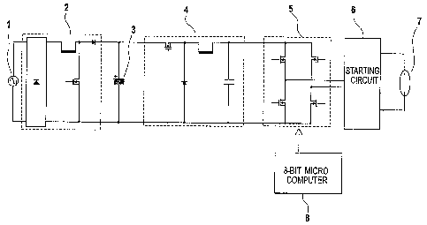
object, there is provided a discharge-lamp lighting device including, as shown
in FIG. 1, a DC/DC converter 4 that converts a power supply voltage of a DC
power supply (smoothing capacitor 3) and stably lights a high-intensity
discharge lamp 7, a DC/AC inverter 5 that converts the DC voltage into an
AC voltage, and a starting circuit 6 that has a resonance circuit composed of
at least one or more capacitors 66 and inductors 65 as shown in FIG. 4 and
supplies an output from the DC/AC inverter 5 to the high-intensity discharge
lamp 7. Upon start-up of the high-intensity discharge lamp 7, a period A
during which the starting circuit 6 applies a high voltage generated by
resonance operation of the resonance circuit to the high-intensity discharge
lamp 7 when the DC/AC inverter 5 outputs a high-frequency voltage, and a
period B during which the DC/AC inverter 5 applies a
low-frequency-square-wave voltage or a DC voltage to the high-intensity
discharge lamp 7 via the starting circuit, are output in an alternate manner
as shown in FIG. 7. While the high-intensity discharge lamp 7 is lighted, the
DC/AC inverter 5 applies the low-frequency-square-wave voltage to the
high-intensity discharge lamp 7 via the starting circuit. The period A for
applying the high voltage by the resonance operation is set to about a time
enough for a high-intensity discharge lamp in an initial aging stage to cause
a dielectric breakdown, and a period C for outputting the high-voltage
generating period and the low-frequency-square-wave voltage or DC voltage
CA 02652927 2008-11-20
4
generating period in the alternate manner is set to about a time enough for a
high-intensity discharge lamp in a life's last stage to cause the dielectric
breakdown.
BRIEF DESCRIPTION OF THE DRAWINGS
[0008]
FIG. 1 is a circuit diagram according to a first embodiment of the
present invention.
FIG. 2 is a circuit diagram of a conventional impulse starting
circuit.
FIG. 3 shows operational waveforms of the starting circuit in FIG.
2.
FIG. 4 is a circuit diagram of a resonant step-up starting circuit
used in the present invention.
FIG. 5 shows operational waveforms of the starting circuit in FIG.
4.
FIG. 6 also shows operational waveforms of the starting circuit in
FIG. 4.
FIG. 7 shows an operational waveform in the first embodiment of
the present invention.
FIG. 8 is an explanatory diagram of the first embodiment of the
present invention.
FIG. 9 is also an explanatory diagram of the first embodiment of
the present invention.
FIG. 10 is an explanatory diagram of a second embodiment of the
present invention.
FIG. 11 is an explanatory diagram of a third embodiment of the
present invention.
FIG. 12 is a circuit diagram according to a fourth embodiment of
the present invention.
CA 02652927 2008-11-20
BEST MODE FOR CARRYING OUT THE INVENTION
[0009]
(First Embodiment)
5 FIG. 1 shows a circuit structure of a discharge-lamp lighting
device according to a first embodiment of the present invention. A
voltage output obtained from an AC power supply 1, which supplies
commercial power supply voltage, and then rectified by a rectifier 2, is
smoothed by a capacitor 3, and a DC/DC converter 4 controls a lamp
current or lamp power necessary for stably lighting a high-intensity
discharge lamp 7. The output controlled to a desired value is converted
into a low-frequency square wave output by the DC/AC inverter 5, and
then supplied to the high-intensity discharge lamp 7. Upon start-up of
the high-intensity discharge lamp 7, it requires a dielectric breakdown
induced by a high impulse voltage of several to tens of W. A
high-voltage pulse is generated from a starting circuit 6 to start the
high-intensity discharge lamp 7.
[0010]
A start-up process of the high-intensity discharge lamp is
characterized by a dielectric breakdown between electrodes and its
subsequent transition from glow discharge to arc discharge, and control
needs to be made so that energy is supplied in optimum conditions
depending on each operating state in order to achieve a smooth transition
from a start-up state to a stable lighting state. Therefore, the
high-intensity discharge lamp is different from a fluorescent lamp in that
the fluorescent lamp can start with a dielectric breakdown requiring a
relatively low voltage of hundreds of V and also quickly shifts to a steady
discharging state. Accordingly, control made in the start-up process of
the high-intensity discharge lamp is more complex than that of the
fluorescent lamp.
CA 02652927 2008-11-20
6
[0011]
FIG. 2 shows an example (comparative example) of the starting
circuit 6. This circuit is an impulse starting circuit 64 that uses a pulse
transformer to increase a voltage applied to a primary side thereof several
ten to hundred times and forwarding the increased voltage to a secondary
side of the transformer, and that applies a high-voltage pulse having a
relatively narrow width to the high-intensity discharge lamp 7. A series
circuit of a capacitor 61 and a primary side 62a of a pulse transformer 62,
a series circuit of a switching element 63, and a series circuit of the
high-intensity discharge lamp 7 and a secondary side 62b of the pulse
transformer 62, are connected to an output end of the DC/AC inverter 5
provided at a preceding stage. Voltage charged in the capacitor 61 is
discharged all at once by the switching element 63 via the primary side
62a of the pulse transformer 62, at which time the voltage applied to the
primary side 62a is raised up to several ten to hundred times and then
forwarded to the secondary side 62b, so that a high-voltage pulse of
several to tens of kV can be applied to the high-intensity discharge lamp
7.
[0012]
In this case, a waveform of the high-voltage pulse is as shown in
FIG. 3(a), and a relatively narrow pulse width, that is, relatively small
pulse energy is obtained. In an actual case, this high-voltage pulse is
superimposed upon a low-frequency square wave output at stable lighting
time and fed to the high-intensity discharge lamp 7, as shown in FIG. 3(b).
A point S in FIG. 3(c) indicates that the dielectric breakdown has occurred
in the high-intensity discharge lamp 7 and it has started. Subsequent to
the point S, the high-voltage pulse is terminated.
[0013]
FIG. 4 shows another example (embodiment example) of the
starting circuit 6. This circuit is a resonant step-up starting circuit 67
CA 02652927 2008-11-20
7
that is a resonance circuit composed of an inductor and a capacitor and
generates a high-frequency voltage in the neighborhood of a resonance
frequency of the resonance circuit by the DC/AC inverter 5 provided at
the preceding stage, and that applies a high-voltage pulse having a
relatively broad width to the high-intensity discharge lamp 7. A series
circuit of an inductor 65 and a capacitor 66 is connected to the output
end of the DC/AC inverter 5 of the preceding stage, and the capacitor 66
is connected in parallel with the high-intensity discharge lamp 7.
[0014]
The DC/AC inverter 5 generates the high-frequency voltage in the
neighborhood of the resonance frequency of the resonance circuit
composed of the inductor 65 and the capacitor 66, which induces a
resonant step-up voltage across the inductor 65 or the capacitor 66,
thereby enabling an application of the high-voltage pulse of several to tens
of kV to the high-intensity discharge lamp 7. In this case, a waveform of
the high-voltage pulse is as shown in FIG. 5(a), and a few pulses are
output together. A start-up condition of the high-intensity discharge
lamp 7 is a relatively broad pulse width, that is, relatively large pulse
energy. Note that, the inductor 65 can have a structure of a step-up
transformer such as the foregoing pulse transformer 62 to apply a voltage
several times as large as the primary side voltage.
[0015]
The waveform of the high-voltage pulse in FIG. 5(a) corresponds to
the case that an operational frequency of the DC/AC inverter 5 is fixed to
a value in the neighborhood of the resonance frequency of the inductor 65
and the capacitor 66. In actual cases, the operational frequency of the
DC/AC inverter 5 can be swept near the resonance frequency in order to
absorb variations in the resonance frequency of the inductor 65 and the
capacitor 66. At this time, a waveform of the high-voltage pulse is as
shown in FIG. 5(b).
CA 02652927 2008-11-20
8
[0016]
The high-voltage pulse is actually divided into a period of
generating the high-voltage pulse by resonant step-up voltage and a
period of outputting a low-frequency square wave at the stable lighting
time, as shown in FIG. 6(a). Usually at a lighting determination time
(point S in the drawing), a lighting state of the high-intensity discharge
lamp 7 is determined, and when it is not lighted, subsequent outputs are
terminated. This is because the energy of the high-voltage pulse is large
as described earlier and it is therefore not preferable to output this large
energy all the time in terms of safety and durability of components.
Furthermore, from the property of the high-voltage-pulse generating
period, it is set to a relatively long duration so that any types of the
high-intensity discharge lamp 7 can be lighted up. When the
high-intensity discharge lamp 7 causes the dielectric breakdown by the
time of the point S in FIG. 6(b), then is started and lighted up, operation
is continued until the lamp 7 lights stably as the low-frequency square
wave output period. At this time, the high-voltage pulse is terminated in
the same manner as in the previous example.
[0017]
Recent studies have found that the impulse starting circuit 64 in
FIG. 2 and the resonant step-up starting circuit 67 in FIG. 4 have their
respective merits and demerits.
[00181
As described earlier, upon a dielectric breakdown of the
high-intensity discharge lamp 7, the impulse starting circuit 4 sometimes
cannot provide energy sufficient for the dielectric breakdown to the
high-intensity discharge lamp 7 because the high-voltage pulse energy
produced by the impulse starting circuit 4 is small. In contrast, the
resonant step-up starting circuit 67 can ensure the dielectric breakdown
of the high-intensity discharge lamp 7 because the high-voltage pulse
CA 02652927 2008-11-20
9
energy produced by the resonant step-up starting circuit 67 is large.
[0019]
Regarding another start-up condition, which is a transition to the
arc discharge of the high-intensity discharge lamp 7, low-frequency power
supply has been found to be effective in a smooth transition to the stable
lighting of the high-intensity discharge lamp 7. The impulse starting
circuit 64 ensures the smooth transition to the arc discharge because it
supplies the low-frequency square wave to the high-intensity discharge
lamp 7 all the time. In contrast, the resonant step-up starting circuit 67
cannot ensure the smooth transition to the arc discharge because it
generates the high-voltage pulse by high-frequency operation and hence
cannot supply the low-frequency square wave to the high-intensity
discharge lamp 7 at least during the high-voltage pulse generating period.
[0020]
This means that the impulse starting circuit 64 is
disadvantageous in the dielectric breakdown and advantageous in the arc
discharge transition, and the resonant step-up starting circuit 67 is
advantageous in the dielectric breakdown and disadvantageous in the arc
discharge transition, so that the both have good points and bad points.
[0021]
Japanese Patent Application Laid-Open No. 2004-265707 has
proposed an excellent starting method having the advantages of both the
circuits. According to this document, as shown in FIG. 7, a period A of
the resonant step-up starting circuit 67 and a period B of the
low-frequency square wave are alternately repeated during a period C, so
as thereby to combine the advantages of both the circuits in their starting
operations. Specifically, the period A of the resonant step-up starting
circuit 67 ensures the dielectric breakdown performance, and the period
B of the low-frequency square wave ensures the arc discharge transition
performance. The operational frequency of the DC/AC inverter 5 is a
CA 02652927 2008-11-20
high frequency of 10 kHz or more (tens to hundreds of kHz) during the
period A, and is a low frequency below 1 kHz (100 Hz to several hundreds
of Hz) or a direct current during the period B.
[0022]
5 Recent studies have found that it is important to set each of the
periods A, B, and C described in Japanese Patent Application Laid-Open
No. 2004-265707 to their respective optimum lengths of time, and also
that, when the optimum lengths are not set, factors of the foregoing
demerits of the impulse starting circuit 64 and the resonant step-up
10 starting circuit 67 become seriously apparent. Specifically, when the
period A of the resonant step-up starting circuit 67 is too short, the
foregoing demerit of the impulse starting circuit 64 becomes apparent,
resulting in the smooth transition to the arc discharge, but also in
deficient dielectric breakdown performance. In contrast, when the period
A of the resonant step-up starting circuit 67 is too long, the foregoing
demerit of the resonant step-up starting circuit 67 becomes apparent,
resulting in a satisfactory dielectric breakdown, but also in a non-smooth
transition to the arc discharge.
[0023]
In addition, recent studies have found that the high-intensity
discharge lamp 7 is relatively easy to start in an initial aging stage (e.g.,
0
to 100 hours) right after product shipment, but as the end of service life
(e.g., 10,000 hours) approaches, the high-intensity discharge lamp 7
becomes gradually difficult to start because of electrode sputtering and
the like, as shown in FIG. 8.
[0024]
More Specifically, when a time required for the dielectric
breakdown of a discharge lamp in the initial aging stage is set as the
period A, a discharge lamp in a life's last stage cannot obtain sufficient
dielectric breakdown performance. In contrast, when a time required for
CA 02652927 2008-11-20
11
the dielectric breakdown of the discharge lamp in the life's last stage is set
as the period A, the discharge lamp in the initial aging stage cannot
obtain sufficient arc discharge transition performance. In consideration
of this inconsistency, it is very important that this lighting circuit
provides
satisfactory dielectric breakdown performance and arc discharge
transition performance comprehensively to all high-intensity discharge
lamps that can be handled in combination in real markets, and also
ensures reliable starting performance.
[0025]
Setting of the periods A and C according to the present invention
will be described with reference to FIG. 9. As shown in FIG. 9, a
dielectric-breakdown required time AA for a general high-intensity
discharge lamp in the initial aging stage and a dielectric-breakdown
required time CC for the high-intensity discharge lamp in the life's last
stage are definite. Therefore, the period A for applying the high voltage
by resonance operation in FIG. 7 is set approximately to the
dielectric-breakdown required time AA for the general high-intensity
discharge lamp in the initial aging stage, and also the period C for
alternately outputting the high-voltage generating period and the
low-frequency-square-wave voltage or DC voltage generating period is set
approximately to the dielectric-breakdown required time CC for the
high-intensity discharge lamp in the life's last stage. Note that "set
approximately to" means, for example, that "the period A is the same
length as the time AA, and the period C is the same length as or longer
than the time CC", or that "the period A is the same length as or longer
than the time AA, and the period C is the same length as or longer than
the time CC".
[0026]
The period B for outputting the low-frequency square wave or the
DC output is set to a length of time corresponding to the low-frequency
CA 02652927 2008-11-20
12
square wave at normal lighting time or longer than this length of time.
[0027]
Setting of these periods is realized when a control circuit 8 of the
DC/AC inverter 5 controls polarity inversion of the DC/AC inverter 5 in
each period. In the period A, the DC/AC inverter 5 is operated at a high
frequency (tens to hundreds of kHz) in the neighborhood of the resonance
frequency of the starting circuit 6 thereby to output a resonant step-up
high voltage, and in the period B, the DC/AC inverter 5 is operated at a
low frequency (100 Hz to several hundreds of Hz) or by a direct current
thereby to output a low-frequency square wave voltage or a DC voltage.
The period C is composed of these alternately repeated periods A and B.
[0028]
The control circuit 8 is usually composed of an 8-bit
microcomputer and the like, and operational frequencies and durations of
these periods A, B, and C can be set arbitrarily according to a
microcomputer program.
[0029]
Note that the DC/AC inverter 5 can be designed not only for
operation at a fixed frequency near the resonance frequency but also for
operation at a sweep frequency, as described earlier in the conventional
example.
[0030]
In this embodiment, the DC/DC converter 4 is made up of a
step-down chopper circuit; however, as disclosed in Japanese Patent
Application Laid-Open No. 2004-265707, the DC/DC converter 4 can be
made up of a step-up chopper circuit or a flyback-type step-up/down
converter circuit. Furthermore, the DC/DC converter 4 and the DC/AC
inverter 5 are independent of each other; however, as disclosed in
Japanese Patent Application Laid-Open No. 2004-265707, a full-bridge
circuit or a half-bridge circuit having the both can be used. For example,
CA 02652927 2008-11-20
13
upon an output of the low-frequency square wave voltage, a pair of
switching elements on a low-potential side of the full-bridge circuit are
turned ON and OFF alternately at a low frequency, and another switching
element diagonally opposite to the ON-state switching element on a
high-potential side is turned ON and OFF at a high frequency, so that the
functions of both the DC/DC converter and the DC/AC inverter can be
achieved by the single full-bridge circuit.
(0031]
(Second Embodiment)
In addition to the explanation for the first embodiment, a second
embodiment will be described with reference to FIG. 10. In the first
embodiment, when the period A in FIG. 7 is set to a value that is too long
in duration, the aforementioned demerit of non-smooth transition to the
arc discharge that is observed in the starting circuit 67 becomes apparent,
and therefore the value of the period A needs to be considered very
carefully. When a time at which the transition to the arc discharge is
getting non-smooth is represented by a time D, the period A needs to
satisfy the condition in the first embodiment and also needs to be shorter
than the time D at which the transition to the arc discharge is getting
non-smooth. In this embodiment, the high-frequency operating period A
in FIG. 7 is set to a length of time not less than the dielectric-breakdown
required time AA for the general high-intensity discharge lamp in the
initial aging stage, and not more than the time D at which the transition
to the arc discharge is getting non-smooth. The period B is set to a
length of time corresponding to the low-frequency square wave during
normal lighting time or shorter. Setting of these periods is controlled by
the microcomputer of the control circuit 8 as in the same manner as the
first embodiment.
[0032]
(Third Embodiment)
CA 02652927 2008-11-20
14
In addition to the explanation for the first embodiment, a third
embodiment will be described with reference to FIG. 11. FIG. 8
explained above shows sampling data of discharge lamps that have
already been manufactured on a commercial basis at the present time.
In consideration of the present situation where novel discharge lamps
with compact size, high efficiency, and the like are released one after
another to the market, it is necessary to fully consider that the time
required for the dielectric breakdown of these lamps becomes long after
they are designed. Specifically, as shown in FIG. 11, in consideration of
a risk of distribution of high-intensity discharge lamps having more
difficulty in the dielectric breakdown than samples of high-intensity
discharge lamps that can be tested at the design time (a sample-data
maximum value MX 1 of discharge lamps already commercially
manufactured, a sample-data estimated maximum value MX2 of new
discharge lamps expected to be commercially manufactured), the time
required for the dielectric breakdown needs to be set a little longer.
[0033]
When the period A in FIG. 7 is set to a value that is too long in
duration, the aforementioned demerit of non-smooth transition to the arc
discharge observed in the starting circuit 67 becomes apparent, and
therefore the value of the period A needs to be considered carefully. As a
result of investigation, the transition to the arc discharge of the discharge
lamp is not performed smoothly when the period A is 10 msec. or longer.
[0034]
An estimated time of the period C in FIG. 7 greatly varies because
the period C is the time until which the discharge lamp in the life's last
stage causes the dielectric breakdown. In general, generation of a
high-voltage waveform as seen in the period C involving the period A for 1
sec. or longer is not preferable in terms of reliability of electronic
components used in this lighting circuit and safety of users.
CA 02652927 2008-11-20
[0035J
Accordingly, the period A in FIG. 7 is set to 1 to 10 msec., and the
period C in FIG. 7 is set to 10 msec. to 1 sec. The period B is set to a
length of time corresponding to the low-frequency square wave during
5 normal lighting time or longer. Setting of these periods is controlled by
the microcomputer of the control circuit 8 in the same manner as the first
embodiment.
[0036]
(Fourth Embodiment)
10 A fourth embodiment will be described with reference to FIG. 12.
Referring to FIG. 12, a discharge-lamp tube voltage detector circuit 9 is
additionally provided as means for determining accumulated lighting time
of the high-intensity discharge lamp 7, so that the accumulated lighting
time can be determined to be getting long when a tube voltage rises.
15 This utilizes a property of the discharge lamp that the tube voltage
thereof
rises as the end of service life approaches. The tube voltage detected by
the tube voltage detector circuit 9 is informed to the control circuit 8, and
this information is stored in a non-volatile memory, so that the period C
can be set longer as the end of service life approaches, that is, as the
accumulated lighting time becomes long.
[0037]
In addition, a non-volatile timer function (by which timer count
value is stored even when power is turned OFF) can be provided to the
control circuit 8 to determine the accumulated lighting time of the
discharge lamp, by counting the lighting time of the discharge lamp with
this timer and resetting the timer at lamp replacement time.
[0038]
(Fifth Embodiment)
The discharge-lamp lighting devices according to the first to the
fourth embodiments can be built in a luminaire to which a high-intensity
CA 02652927 2008-11-20
16
discharge lamp is attached, or can be used as a stabilizer externally
provided to a lamp fitting. Furthermore, such luminaire can be
combined with a human sensor or a brightness sensor to provide an
illumination system that controls light output depending on sensor
output. Moreover, such luminaire can be combined with a timer to
provide an illumination system that controls light output depending on
time zones. Furthermore, such luminaire can be used for a
projection-type image display device and a headlight of a vehicle that use
a high-intensity discharge lamp as a light source, and in this case, the
light output quickly rises advantageously because of smooth starting of
the discharge lamp.
INDUSTRIAL APPLICABILITY
[0039]
According to the present invention, there is provided a
discharge-lamp lighting device that offers optimum dielectric breakdown
performance and arc discharge performance of a high-intensity discharge
lamp and realizes smooth starting thereof in a starting process, by
associating a period for applying a high voltage by resonance operation, a
period for applying a low-frequency-square-wave voltage or a DC voltage,
and a cycle of these repetitive periods, with a time required for a dielectric
breakdown of a discharge lamp both in an initial aging stage and in a
life's last stage.