Note: Descriptions are shown in the official language in which they were submitted.
CA 02653020 2013-05-16
1 Addressing Device and Method, and Converter
2
3 Description:
4
The present invention relates to a device that is provided as a bus
participant, that is, a field
6 device, a method for addressing, and a converter.
7
8 AS (actuator sensor) interface as a bit-oriented field bus on the lowest
level of the
9 automatization pyramid known from:
- the R. Becker (Ed.) publication AS Interface, the Design Approach in
Automation,
11 Gelnhausen (2002): ASInternational Association, in particular Chapter
3.2,
12 - German Patent Application No. DE 197 43 981 Al (1999),
13 - European standard EN 50295 (1999), and
14 - the presentation "The AS-Interface Innovation Step 3.0" of the AS
International
Association from 06/28/2005.
16 It is optimized for the connection of simple sensors, actuators, and field
devices that exchange
17 only a few information bits with the control. Thus, only four information
bits are able to be
18 transmitted from the master to the slave and back again in a data message
from the AS
19 interface.
21 However, modern field devices, as used in particular in systems having
decentralized control
22 technology, often require numerous parameters that may be variably adjusted
to optimize the
23 function of the field devices.
24
Moreover, modern field devices may often collect diagnosis and service
information that
26 supports a quick removal of problems in the event of a malfunction. This
includes electronically
27 transmittable data not only about the product, such as manufacturer, model
designation,
28 production date, state of firmware, but also about the operation, such as
operating hours,
29 number of start/stop procedures, overload states, and more of the like.
1
22388231.2
CA 02653020 2012-03-15
1 Other field devices, for operating and observing, for example, have a
simple display on which
2 measurement data are output and a keyboard field via which commands may
be input to the
3 control, for example. Here too, different byte-oriented and bit-oriented
functions are logically
4 assigned to each other, the first ones being used for the display and the
last ones being used
for the keys.
6
7 To accommodate this condition, specification version 3.0 introduces slave
profiles, which are
8 provided with both bit-oriented and byte-oriented data exchange
mechanisms, see the cited
9 publication AS Interface, the Design Approach in Automation, for example.
The profile S-7.A.5 is
mentioned by way of example in this instance. In this profile, two bits are
used in each instance
11 for a serial data exchange; thus, only one or two bits remain for the
quick bit-oriented data
12 exchange. This in turn is too little for many applications ¨ e.g., in
drive engineering.
13
14 The present invention is based on the objective of refining the data
exchange in a bus system in
a manner that is simple and low in errors.
16
17 Important features of the present invention in the device provided as a
bus participant are that it
18 is connected by a connection to a bus, in particular to an electric
cable, to a current bus, or
19 connected via an antenna to air, means for providing two or more bus
participants being
included, and means being included for assigning to the two or more bus
participants the data
21 that is flowing in and/or is exchanged via the connection. Such devices
that are provided as bus
22 participants are also called field devices. An advantage of the present
invention is that two or
23 more bus participants are able to be connected to a bus via one
connection, which simplifies the
24 cabling. Also, by providing a plurality of bus participants, it is
possible to exchange fast, bit-
oriented data on the one hand, and slow, byte-oriented, complex data on the
other hand. Thus,
26 the data exchange between master and slave in a field bus system is
refined such that it is
27 possible to use different data exchange mechanisms as a function of
requirements in a manner
28 that is simple and low in errors. It is furthermore advantageous that a
field device contains a
22214291.1
2
CA 02653020 2013-05-16
1 group of slaves and thus may exchange different data types with a master via
different data
2 exchange mechanisms.
3
4 Important features of the present invention in the device connected to a bus
are that it
implements one logical slave, in particular, a bus participant, in a first
mode, and at least two
6 logical slaves, in particular, bus participants, in a second mode. Thus, it
is advantageously
7 made possible to switch between different modes, depending on requirements
for data
8 exchange, for example. In particular, an easily manipulable mode may be
selected for an
9 initialization of the device or the integration into the field bus system,
for example, while a
complex mode having a plurality of bus participants may be selected for a
complex data
11 exchange.
12
13 In an additional advantageous refinement, exactly one logical slave, in
particular a bus
14 participant, is implemented in the first mode. In this context, it is
advantageous that the initial
operation, in particular, log on in the field bus system or address
assignment, may be carried
16 out simply.
17
18 In an additional advantageous refinement, the bus is a field bus, in
particular CAN (controller
19 area network), CAN-Open, DeviceNet, Profibus (process field bus), INTERBUS,
AS (actuator
sensor) interface, Ethernet, Wireless-LAN (wireless local area network), EIB
(European
21 installation bus), LCN (local control network). In this context, it is
advantageous that the bus
22 participant is able to be connected to a standardized bus. Thus, the device
according to the
23 present invention may be used in a modular manner in conventional systems,
in particular in
24 systems having decentralized technology.
26 The present invention may be used particularly advantageously in bus
systems that include at
27 least one master and a plurality of slaves, the master assigning addresses
to the slaves.
28
29 In an additional advantageous refinement, the first mode is a standard
addressing mode; in an
additional advantageous refinement, the second mode is an expanded addressing
mode. In this
31 context, it is advantageous that, in particular in the event of a
connection to an AS interface
32 bus, in the first mode it is possible to assign an address that may be used
in the second mode
33 for a plurality of bus participants or logical slaves, since in the
expanded addressing mode
34 different slaves may be addressed using one address in the different
cycles.
3
22388231.2
CA 02653020 2008-11-12
1 In an additional advantageous refinement, the device includes a reversing
logic that shifts the
2 device from the first to the second mode when a standard address is
switched, in particular
3 from a delivery address or from address "0" to another address value. In
this context, it is
4 advantageous that it is possible to switch the modes through standard
processes on the bus. It
is thus possible to avoid enlarging the quantity of instructions and commands
relayed via the
6 bus.
7
8 In an additional advantageous refinement, the device operates in the first
mode when the
9 address "0" is assigned, and in the second mode when an address other than
"0" is assigned.
In this context, it is advantageous that a procedure that is required anyway,
to wit the
11 assignment of an address to a device that is identified by address "0" as
newly connected to the
12 bus, is able to be used for switching over to the more complex mode. Thus,
in a simple method,
13 addresses are able to be assigned by a master or with the aid of a
conventional addressing
14 device. When the address "0" is selected as a feature that distinguishes
functions, it is
particularly advantageous that AS interface slaves occupy this address during
delivery. Thus,
16 up to the addressing, the device according to the present invention
presents itself as a standard
17 slave vis-à-vis the master when integrated into an AS interface network.
Thus, advantageously,
18 for the user this is no different than addressing a normal slave, in
particular possibly an AS
19 interface slave. After addressing, the second mode, which is provided for
the main operation of
the field device, is immediately available. Furthermore, in the second mode,
in the expanded
21 addressing mode, the assigned address may advantageously be used, as
described in DE 102
22 06 657 Al, for example. Thus, only one address allocation is required for a
plurality of slaves or
23 bus participants. Thus, double addressing may advantageously be avoided.
24
In a further advantageous refinement, the at least two logical slaves have
profiles that differ
26 from each other. Thus, the slaves implemented may be used for different
data transmission
27 mechanisms. For example, bit-oriented functions may be transmitted to one
slave and byte-
28 oriented functions to another slave.
29
Important features of the present invention for the device for connecting to a
bus are that the
31 device includes a computer, the state machine of at least two bus
participants being
32 represented in the computer. In this context, it is advantageous that two
or more bus
33 participants and/or logical slaves may be implemented.
34
21826128.1 4
CA 02653020 2008-11-12
1 In another advantageous refinement, the device includes one slave IC and the
computer
2 connected to it, in particular a microprocessor having memory, the slave IC
being able to be
3 used in the transparent mode. In this context, it is advantageous that a
communication between
4 bus and microprocessor and an implementation of a plurality of slaves is
made possible in a
simple and cost-effective manner.
6
7 In an additional advantageous refinement, the bus participant is developed
as an AS interface
8 slave or another field bus slave. In this context, it is advantageous that
standardized bus
9 systems are able to be used, in particular when an AS interface bus is used.
11 Important features of the present invention in the method for addressing a
device provided as a
12 bus participant are that two logical slaves are included,
13 wherein
14 - the device is provided with a standard address, in particular address
"0," before the
addressing and operated in a first mode, in particular standard addressing
mode,
16 - another address is assigned to the device,
17 - and then the device implements at least two logical slaves after
address assignment.
18 It is advantageous that the addressing of such a device is able to be
performed with every
19 addressing device that is already on the market. It is furthermore
advantageous that the
address "0" constitutes the standard address during delivery or new log on in
the bus system of
21 a bus participant, and it is standard for it to be followed by an address
allocation by a master. In
22 particular, the master or alternatively the user of such a device has to
perform only one
23 addressing procedure for the at least two logical slaves.
24
In an additional advantageous refinement, in the expanded addressing mode, the
slaves are
26 addressed by the assigned address, in alternation, in sequential cycles, as
A address or B
27 address. In this context, it is advantageous that in the slave in the
standard addressing mode
28 the same address space is able to be occupied as is able to be occupied in
the at least two
29 logical slaves in the expanded addressing mode, for example. The addressing
procedure is
thus advantageously able to be performed without the risk of the double
addressing.
31
32 Important features of the present invention for the converter are that a
device for connecting to
33 a bus is integrated. In this context, it is advantageous that in the
converter, means for
21826128.1 5
CA 02653020 2008-11-12
1 communicating with a bus system are able to be provided. Thus, the converter
is
2 advantageously able to be used in systems using decentralized technologies.
3
4 In a further advantageous refinement, the microprocessor of the device for
connecting to a bus
is integrated into the control of the converter, in particular into the
control of the power
6 electronics of the converter. In this context, it is advantageous that the
computing capacity that
7 already exists in the control of the converter may be used for the
implementation of the logical
8 slave. This advantageously results in a compact design having few
components.
9
In an additional advantageous refinement, connection means for connecting
actuators and/or
11 sensors and/or a bus, for example, MOVILINK , and/or switching outputs
and/or [sic] are
12 included, it being possible for the bus to control or read these connecting
means and/or
13 switching outputs. In this context, it is advantageous that the converter
having the integrated
14 means may also be used as a slave to process the simplest functions and
also as a node in the
bus network, in addition to its eponymous function.
16
17 The dependent claims yield additional advantages.
21826128.1 6
CA 02653020 2008-11-12
1 List of reference symbols
2
3 1 field device
4 2 AS-i-line
3 slave
6 3A first slave
7 3B second slave
8 4 connection line
9 5 internal line
6 contact
11 7 internal line
12 8 connection
13 10 slave IC
14 11 microprocessor
12, 13, 14 internal data line
16 30 state in the first mode
17 31 RESET signal
18 32 standard addressing signal
19 33 state in the second mode
34 additional state in the second mode
21 35 bus command, sensor data, or actuator command
22 50 converter
23 52 motor
24 53 connecting point
54 field bus
26 55 connection line
27 56 control
28 58 slave
29 60 power electronics
62 actuator
31 64, 66 sensor
32 68 bus
21826128.1 7
CA 02653020 2008-11-12
1 The present invention will now be explained in greater detail with the aid
of figures:
2
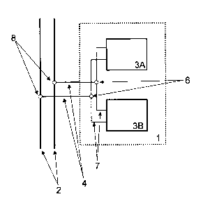
3 The figures show:
4 - Figure 1 the function diagram of a field device after assignment of
the address "0"
- Figure 2 the function diagram of a field device according to the present
invention after
6 assignment of an address other than "0"
7 - Figure 3 a schematic of a field device according to the present
invention,
8 - Figure 4 the state machine of a microprocessor according to the
present invention
9 - Figure 5 a converter having a motor as a field device according to
the present invention.
11 Figure 1 shows the function diagram of a field device 1 according to the
present invention if it
12 has been assigned the address "0." This is the case, for example, if field
device 1 is newly
13 installed in the delivery state or is re-installed in the AS interface
network after a servicing.
14
Field device 1 is connected to an AS interface line 2 via a connection line 4
and a connection 8
16 at a connection point. It participates in the AS interface network via this
connection line 4 as
17 though connection lines 4 were connected via inner lines 5 to a slave 3
having a standard
18 profile, for example, the profile S-7.F.F. Here, slave 3 and inner lines 5
are virtual, that is, field
19 device 1 simulates the function illustrated.
21 With the aid of the address "0," a master that is also connected to the AS
interface line may
22 now detect field device 1 as a new participant and assign a free address to
it, in the manner
23 typical of AS interfaces, as is described in DE 197 43 981 Al, for example.
Alternatively, this
24 address assignment may be carried out with a conventional addressing
device.
26 Figure 2 shows the function diagram of a field device 1 according to the
present invention if this
27 has been assigned an address other than "0." This may be the case, for
example, if field device
28 1 was detected by a master as a new participant and occupied with a free
address.
29
Field device 1 is connected to an AS interface line 2 via a connection line 4
at a connection 8 in
31 a connection point. In contrast to the case illustrated in Figure 1, it
participates in the AS
32 interface network via this connection line as a bus participant of the bus
system as though
33 connection lines 4 were connected via inner lines 7 and an inner branching
6 to two slaves 3A
34 and 3B. Advantageously, these slaves have different profiles, for example,
slave 3A the profile
21826128.1 8
CA 02653020 2008-11-12
1 S-7.A.7 for a quick binary and thus bit-oriented input and output, and slave
3B profile S-7.A.5
2 for additional digital and thus byte-oriented input and output.
3
4 The AS interface network is now operated in the expanded addressing mode,
and slave 3A
responds to the address of field device 1 in the A cycle, while slave 3B
responds to the address
6 of field device 1 in the B cycle.
7
8 Field device 1 thus simulates the connection of two slaves 3A and 3B to the
AS interface
9 network, slave 3A using the address of field device 1 as A address, while
slave 3B uses this
address as B address. Thus, a logical slave at address "0" becomes two or more
logical slaves
11 having profiles that may be predefined arbitrarily if the address is not
"0."
12
13 In an additional exemplary embodiment according to the present invention,
field device 1
14 simulates the connection of three, four or more slaves via connection line
4 if the address "0"
was not assigned to it. For the simulation of more than two slaves, more than
one address is
16 assigned to the field device, which are able to be used in the expanded
addressing method
17 analogously to the example from Figure 2, or an addressing mode is used,
which has three,
18 four, or more different cycles according to the type of the expanded
addressing mode.
19
Figure 3 shows an exemplary embodiment of a field device according to the
present invention.
21 A field device 1 is connected via connection lines 4 to an AS interface
line 2 and includes a
22 conventional slave IC 10, that is, an integrated circuit, and a
microprocessor 11. Slave IC 10 is
23 operated in the transparent mode and thus relays the data obtained from AS
interface line 2 via
24 connection lines 4 to microprocessor 11 via an internal data line 12 and
relays data received
from microprocessor 11 via an additional internal data line 14 to AS interface
line 2.
26 Additionally, this microprocessor 11 obtains from slave IC 10 the clock
signal via an additional
27 internal data line 13. The state machine of at least one AS interface slave
is represented in the
28 firmware of microprocessor 11, that is, the finite machine, which models
all possible states of
29 the AS interface slaves and the permitted transitions between these states.
Such state
machines are described in A. Hunt and D. Thomas: State Machines, IEEE Software
31 November/December 2002, p 10-12. Thus, two or more logical slaves are able
to be
32 implemented in microprocessor 11, and microprocessor 11 may simulate a
predefined number
33 of logical slaves depending on the assigned address, which is transmitted
from an addressing
34 device or the master via slave IC 10.
21826128.1 9
CA 02653020 2008-11-12
1
2 Figure 4 illustrates schematically the state machine of a microprocessor 11
as it may be
3 implemented in Figure 3. After a RESET signal 31 or in the delivery state,
microprocessor 11 is
4 in a first mode 30, in which it is assigned an address via standard
addressing signals 32 from
the AS interface bus and enters a state 33 of a second mode. This transition
may be brought
6 about by a reversing logic. The second mode includes this state 33 and
additional states 34,
7 which at least include the possible states of two logical slaves 3A, 3B. In
particular, state 33
8 therefore describes two logical slaves that may be operated in the expanded
addressing mode,
9 an each one [sic] in one of the two cycles and using the address assigned by
standard
addressing signal 32. Between these states 33, 34 transitions 35 are brought
about through
11 bus commands, data from sensors or actuators connected to the
microprocessor, or through
12 sending commands to actuators, as necessary and typical for the
implementation of the at least
13 two logical slaves 3A, 3B.
14
Figure 5 shows a use according to the present invention of a field device from
Figure 1 through
16 4. The field device is a converter 50, which is connected to an
electromotor 52 and which
17 controls or regulates it. Converter 50 is furthermore connected to a field
bus 54, an AS interface
18 bus, for example, more exactly one connection line 55 connecting a slave 58
included by
19 converter 50 to field bus 54 via a connecting point 53. Slave 58 is thus
integrated in converter
50; it is operated in the transparent mode. A microprocessor, which is
designed as control 56 of
21 converter 50, takes on the data forwarded by the slave according to the
array in Figure 3 and
22 processes it with the aid of a state machine stored in it as shown in
Figure 4. Control 56 is
23 simultaneously used for the control or regulation of motor 52, which is
functionally typical for a
24 converter, to wit, through the control of a power electronics 60 connected
to the latter.
Microprocessor 11 from Figure 3 is thus advantageously integrated into control
56 of converter
26 50, which is necessary anyway and which is therefore present. Actuators 62
and sensors 64, 66
27 are connected to control 56 directly or via an additional bus 68 and are
possibly integrated in
28 motor 52, as shown exemplarily for sensor 66. Converter 50 is thus designed
as a field device,
29 as is advantageous for applications of the decentralized technology.
31 In particular, means are integrated in converter 50 that allow for a use of
converter 50 as a bus
32 participant. The provision according to the present invention of two
logical slaves by a
33 corresponding state machine in control 56 particularly advantageously makes
it possible on the
34 one hand for binary data for the control of actuators 62 or sensors 64, 66
to be exchanged
21826128.1 10
CA 02653020 2008-11-12
1 between field bus 54 and converter 50, and on the other hand for byte-
oriented data, for
2 example, in the form of parameters for converter 50 or of commands for
operating motor 52 or
3 in the form of information about the state of converter 50 or motor 52, to
be transferred.
4
In an additional exemplary embodiment according to the present invention,
instead of the AS
6 interface bus, another field bus, in particular CAN, CAN-Open, DeviceNet,
Profibus,
7 INTERBUS, Ethernet, Wireless-LAN, EIB, LCN [is provided].
8
21826128.1 11