Note: Descriptions are shown in the official language in which they were submitted.
CA 02653842 2008-11-27
WO 2007/142960 PCT/US2007/012726
Laser Scanning Digital Camera With Simplified Optics and Potential for
Multiply
Scattered Light Imaging
STATEMENT REGARDING FEDERALLY SPONSORED RESEARCH
The work leading to the invention received support from the United States
federal
government under National Institutes of Health Grant No. EB002346. The federal
government may have certain rights in this invention.
BACKGROUND OF THE INVENTION
The human retina is susceptible to damage from a variety of environmental
factors,
including laser light impact and other trauma, as well as disease. Once
damaged, the cells
responsible for capturing light energy and transducing it into a neural
signal, the
photoreceptors, do not regenerate. In fact, none of the neural cells of the
retina can yet be
made to readily regenerate in the adult human. When damage is severe enough,
there is
permanent vision loss in an area. Healthy photoreceptors do not migrate long
distances
toward the damaged area to replace damaged ones.
If the affected region is in the central macula, known as the fovea, then the
ability to
see fine detail, read at rapid rates, or recognize objects at great distances
may be lost. The
peripheral areas of vision do not have sufficient sampling density to perform
these tasks to
the same degree. Thus, early detection and treatment of potentially sight-
robbing damage are
crucial in maintaining central vision.
One of the chief problems in early detection of damage has been the difficulty
of
imaging a small area of retina. The macula presents a small target-6000
microns. The
portion that is necessary for seeing damage that precludes observation of fine
detail and
reading is even smaller, about 600 microns. To examine this latter portion
properly, it is
1
CA 02653842 2008-11-27
WO 2007/142960 PCT/US2007/012726
desirable to image the central 20 degrees of the macula with sufficient
magnification and
contrast to determine whether an individual is at risk for permanent vision
loss.
The ophthalmoscope or fundus camera has traditionally been used to view and
image
the retina. Originally, these devices flooded the retina with white light.
Subsequent devices
have used selective wavelengths that have been found suitable for viewing or
imaging
particular structures or contrast between structures. Regardless of the
wavelength of light
used, many of the past devices used flood illumination, producing images of
the retina that
often are subject to poor contrast due to long range scatter. The long range
scatter problem
was identified to occur, not only from out of plane tissues, but also from the
biological tissues
that are inherently scattering, especially those within and near the retina.
One well-known method of reducing the long range scatter problem is to replace
a
flood illumination source with a scanning illumination source. Some research
has suggested
that the use of a double scanning optical apparatus that scans both incident
and reflected light
using a horizontal scanning element may be desirable. Scanning with such an
element can be
performed by a rotating multifaceted polygonal reflector, and a vertical
scanning element,
such as a reflecting galvonometer. Such an instrument is able to provide a two-
dimensional
output representative of reflection characteristics of the eye fundus. See,
e.g., US Pat. Nos.
4,768,873 and 4,764,005, as well as US Pat. No. 4,768,874 each disclosing a
laser scanning
ophthalmoscope in which a line beam is scanned across an eye. Such
improvements have
greatly increased the contrast of the images produced, but typically require
expensive, heavy
equipment that must be operated by a specialist.
Improvements on the scanning illumination source technology have been embodied
in
the use of advanced reflectometry techniques with a scanning laser
ophthalmoscope ("SLO")
as developed by the inventor, Ann Elsner, and colleagues. See, for example,
Elsner A.E., et
2
CA 02653842 2011-04-05
al., Reflectometry with a Scanning Laser Ophthalmoscope, Applied Optics, Vol.
31, No.
19 (July 1992), pp. 3697-3710. The SLO is advantageous for quantitative
imaging in that
a spot illumination is scanned in a raster pattern over the fundus, improving
image
contrast significantly over flood illumination. The inventor's SLO technology
can further
eliminate unwanted scattered light by using confocal apertures such as a
circle of variable
diameter or annular apertures, depending on the desired mode. Once the light
is returned
through the confocal aperture, the desired light can then be transmitted to a
detector.
However, the optics used in confocal apertures can increase the complexity of
the system,
and high quality optics are an added expense. Therefore, a method for reducing
or
eliminating unwanted scattered light in a more cost effective manner would be
greatly
appreciated.
Further improvements to increase contrast in retinal imaging systems include
the
extensive use of near infrared light as an illumination source, in lieu of
other wavelengths
or color images, as developed by the inventor and colleagues and described in
Elsner,
A.E., et al., Infrared Imaging of Sub-retinal Structures in the Human Ocular
Fundus,
Vision Res., Vol. 36, No. 1 (1996), pp. 191-205; Elsner, A.E., et al.,
Multiply Scattered
Light Tomography: Vertical Cavity Surface Emitting Laser Array Used for
Imaging
Subretinal Structures, Lasers and Light in Ophthalmology, 1998; Hartnett, M.E.
and
Elsner, A.E., Characteristics of Exudative Age-related Macular Degeneration
Determined
In Vivo with Confocal and Indirect Infrared Imaging, Ophthalmology, Vol. 103,
No. 1
(January 1996), pp. 58-71; and Hartnett, M.E., et al., Deep Retinal Vascular
Anomalous
Complexes in Advanced Age-related Macular Degeneration, Ophthalmology, Vol.
103,
No. 12 (December 1996), pp. 2042-2053. Combining infrared imaging with SLO
allows
the use of reflectometry techniques to view the eye rapidly and noninvasively
because
3
CA 02653842 2011-11-09
infrared light is absorbed less than visible light and scatters over longer
distances. Further, when
implemented with scanning laser devices, infrared and near infrared imaging of
sub-retinal
structure in the ocular fundus has been able to reveal sub-retinal deposits,
the optic nerve
head, retinal vessels, choroidal vessels, fluid accumulation,
hyperpigmentation, atrophy, and
breaks in Bruch's membrane-features that have proven difficult or impossible
to observe
with flood illumination devices. In addition, because infrared illumination is
absorbed by the
tissues less than other wavelengths, much less illumination from the source is
required to create a
high contrast image.
The improvements noted above, and methods for successfully imaging small
retinal
features were combined in United States Patent No. 7,331,699 and PCT
Application No. WO
03/039332. In addition, discussions of using the techniques for detecting and
localizing such
features are described in the publications of the inventor and colleagues:
Elsner, A.E., et al.,
Infrared Imaging of Sub-retinal Structures in the Human Ocular Fundus, Vision
Res., Vol. 36,
No. 1 (1996), pp. 191-205; Elsner, A.E., et al., Multiply Scattered Light
Tomography:
Vertical Cavity Surface Emitting Laser Array Used For Imaging Subretinal
Structures, Lasers
and Light in Ophthalmology, (1998); Elsner, A.E., et al., Foveal Cone
Photopigment Distribution:
Small Alterations Associated with Macular Pigment Distribution, Investigative
Ophthalmology & Visual Science, Vol. 39, No. 12 (November 1998), pp. 2394-
2404;
Hartnett, M.E. and Elsner, A.E., Characteristics of Exudative Age-related
Macular
Degeneration Determined In Vivo with Confocal and Indirect Infrared Imaging,
Ophthalmology, Vol. 103, No. 1 (January 1996), pp. 58-71; and Hartnett, M.E.,
et al., Deep
Retinal Vascular Anomalous Complexes in Advanced Age-related Macular
Degeneration,
Ophthalmology, Vol. 103, No. 12 (December 1996), pp. 2042-2053.
4
CA 02653842 2011-04-05
The systems and techniques described in the inventor's previous patent
applications introduced
a moderately priced, portable system that provided a high contrast, digital
image of the eye that
could be used by non-specialists, such as paramedics or other individuals in
the field. However,
creating a system that is even less expensive, uses standard digital imaging
technology,
includes fewer high precision optics to obtain a high contrast image would be
greatly
appreciated in the art.
In addition, studies have shown that the multiply scattered light images, that
are used
to reveal structures in the deeper retina, can provide more detailed images
that provide
additional diagnostic utility. Further, the use of the infrared spectrum can
be used to image
the retina without dilation of the patient's pupils, and the added potential
for using multiply
scattered light, particularly in cases in which the target of interest falls
below a highly
reflective layer, allow visualization of features difficult to see otherwise.
However, previous
scanning devices, including those embodied in the patent applications
submitted by the
inventor and her colleagues, do not readily utilize this method for producing
an image
without scanning not only the light illuminating the target, but also scanning
the light
returning from the target to the detector, which requires considerable care.
Therefore, a
moderately priced, portable digital retinal imaging device that is capable of
producing
multiply scattered light images would be greatly appreciated in the art.
Existing devices specifically designed for screening of retinal disease that
use flood
illumination with bright lights of shorter wavelengths, and typically acquire
single images at
slow rates, have been shown recently to provide an unacceptable percentage of
gradable
images in the hands of technicians (Zimmer-Galler I, Zeimer R. Results of
implementation of
the DigiScope for diabetic retinopathy assessment in the primary care
environment. Telemed
J E Health. 2006 Apr;12(2):89-98), regardless of the duration of training
(Ahmed J, Ward TP,
5
CA 02653842 2008-11-27
WO 2007/142960 PCT/US2007/012726
Bursell SE. Aiello LM. Cavallerano JD, Vigersky RA. The sensitivity and
specificity of
nonmydriatic digital stereoscopic retinal imaging in detecting diabetic
retinopathy. Diabetes
Care. 2006 Oct;29(10):2205-9.) As discussed above, the embodiments of the
present
application address the issue of inconsistent use in the eye field. Other
issues addressed by
embodiments of the present application include onboard pre-processing of image
and
instrument parameter data for quality assurance and ease of use, addressing
the issue of
alignment of the instrument with respect to the target (e.g., small pupils and
addressing and
other issues regarding the anterior segment of the eye). The present
application further
addresses the prior art issue of failing to capture the images of the best
existing quality, and
failing to operate the instrument with optimal parameters.
Therefore, a moderate cost, portable retinal imaging device that provides for
the use
of a scanning laser device operating with near infrared illumination and which
can allow for
multiply scattered light would be appreciated in the art. Further, such a
device that would
allow for increased ease of use by allowing a greater field of view than just
20 deg visual
angle, greater field of view without sacrificing spatial resolution, as well
as utilizing a non-
proprietary system for producing and saving the digital image, would be
greatly appreciated.
SUMMARY OF THE INVENTION
The present application relates to a device designed as an improved digital
retinal
imaging device. In particular, the present application relates to a laser
scanning digital
camera ("LSDC") intended to be smaller and/or lower in cost than previous
devices, while
retaining a user-friendly format that allows a non-professional to obtain a
high quality digital
retinal image that can be easily stored, transmitted, or printed. In addition,
according to
another embodiment of the present application, the improved digital retinal
imaging device
may be used as a general imaging device or to improve image contrast in
microscopy.
6
CA 02653842 2008-11-27
WO 2007/142960 PCT/US2007/012726
Further, according to another embodiment of the present application, the
additional aperture
configurations and image processing capabilities provide a means for providing
multiply
scattered light images, which are useful for detecting structures that hidden
under highly
reflective tissue (e.g., deep retinal or choroidal disease underlying the
vitreo-retinal interface
and nerve fiber layer). In addition, according to certain embodiments of the
present
application, the device allows for increased illumination and/or light return
at the edges of the
field of view, thereby allowing for a more consistent, high contrast image to
be produced.
Finally, according to certain embodiments of the present application, a system
and device
allow for an increase in field size over previous embodiments, thereby
allowing quality
images to be taken even if the user is not adept at accurately aligning the
imaging device with
the eye.
Therefore, according to one aspect of the present application, the device is
suitable for
providing screening for eye diseases or triage for trauma and can readily
interface with
modem computer technology for remote or telemedicine applications. The device
is able to
operate in extreme heat or cold, when wet, while on a moving surface, and in a
cordless,
battery-powered mode. The device can be manufactured relatively inexpensively
at
significantly less cost than conventional scanning laser ophthalmoscopes.
According to one embodiment of the present application, the device includes an
illumination source, a scanning arrangement, a detection arrangement, a beam
separation
arrangement, and a controller. The scanning arrangement is disposed on an
illumination path
from the illumination source to a target and is operative to scan light passed
through a slit in
the illumination path across a desired focal plane of the target, e.g., the
retinal plane, through
an entrance more narrow than the desired focal plane, e.g., the pupil. The
detection
arrangement is disposed to receive light remitted from the target and
operative to produce an
7
CA 02653842 2008-11-27
WO 2007/142960 PCT/US2007/012726
image. The beam separation arrangement is disposed on a return path from the
target
separated from the illumination path and is operative to receive light
remitted from the target
and to direct remitted light on a detection path to the detection arrangement.
The beam
separation arrangement is configured to space the illumination path and the
return path
sufficiently apart to reduce reflections from sources out of the desired focal
plane and
sufficiently closely to obtain an image of a sufficient desired resolution.
According to one
embodiment, a controller is in communication with the illumination source, the
scanning
arrangement, and the detection arrangement.
In one embodiment, the device differs from previous instruments in that it
features
scanning of one or more light sources, one of which is preferably near
infrared, at a much
reduced cost. The device optionally includes on board digital memory or
another storage
device, such as is used in a digital camera. The instrument is stand-alone in
one embodiment,
and a personal computer is not required to operate the device. Further
optionally, the data are
transmitted to a computer, memory device, or other device including via
wireless broadcast.
A laptop and consumer grade software may be used to access the images if a
computer is
used. In addition, existing or large patient record systems, such as an
electronic medical
record system that can use image data are also a potential means of
distribution or storage of
data.
In one embodiment, the device is minimized in weight or mass and is portable,
so that
it is suitable for use outside of specialized ophthalmological offices and
laboratories.
According to certain embodiments, the device can operate solely on batteries.
The device of
the present application is optionally motorized for remote access, using
either DC operation
or AC operation, as power supply permits. The device can be made to draw its
power though
8
CA 02653842 2008-11-27
WO 2007/142960 PCT/US2007/012726
a single cable, such as through a computer. The computer can be a laptop or
personal data
assistant, which is consistent with use as a portable device.
According to one embodiment of the present application, the digital imaging
device is
operable to provide a high contrast image by using an electronic aperture in
the plane of the
target or in a plane conjugate to the target, in either the input or detection
pathway, or both.
Optionally, the digital imaging device is further capable of providing
multiply scattered light
images by positioning the input and detection apertures in the plane of or
near to the target,
but offset with respect to each other. Alternatively, a multiply scattered
light image may be
obtained by positioning the input and detection apertures conjugate to the
target, but offset
with respect to each other, as described in further detail below. A multiply
scattered light
image provides diagnostic information not readily seen in the reflectance
image, and may be
accomplished by using a rolling shutter feature of a CMOS image array
(discussed in further
detail below) to sample an image line by line. This method leads to a high
contrast image or
a multiply scattered light image according to certain embodiments of the
present application
as discussed in further detail below.
The contrast of an image obtained through the method and/or device of the
present
application can provide details about structures such as retinal blood vessels
that may be
useful as screening or diagnostic data. Near-infrared illumination may be used
to image the
retinal blood vessels, thereby eliminating the need for short wavelength
sources which
require higher power and lead to pupil constriction unless medication is used
to dilate the
pupil. Therefore, the method and device of the present application provide a
more
comfortable experience for the patient, as well as a higher quality image that
may prove more
useful for diagnosis of diseases such as diabetic retinopathy and age-related
macular
degeneration. If more than one wavelength of illumination is used in the
device of the
9
CA 02653842 2011-04-05
present application, each wavelength can correspond to differing amounts of
blood
absorption, thereby allowing hemorrhages and other vascular features to be
visualized in the
comparison image.
According to another aspect, there is provided a digital retinal imaging
device
comprising:
a. an illumination source;
b. a scanning element operable to move a portion of an illumination pathway
created by the illumination source with respect to a target;
c. at least one slit within the illumination pathway of the illumination
source;
and
d. a two dimensional complementary metal-oxide-semiconductor ("CMOS")
detector chip having a rolling shutter functionality.
According to a further aspect, there is provided a digital retinal imaging
device
comprising:
a. an illumination source and scanning element operable to move the
illumination source with respect to a target;
b. a detector array operable to detect and build a first image data set
relative
to the target, and further operable to detect and build a second image data
set
relative to the target;
c. a processor operable to utilize the first image data set and the second
image data set such that each line comprising the first image data set is
compared to a corresponding line on the second image data set in a weighted
manner such that a sharpened image is created.
According to another aspect, there is provided a digital imaging device
comprising:
a. an illumination source and a mechanism to cause a scanning motion of the
illumination with respect to a target;
CA 02653842 2011-04-05
b. a CMOS array operable to select one or more leading lines or lagging lines
with respect to the alignment with an optical axis of a beam from the
illumination source;
c. a processor operable to combine the one or more leading lines and lagging
lines selected and detected to create a multiply scattered image.
According to a further aspect, there is provided a device for digital retinal
imaging,
comprising:
a. an illumination source that fluoresces when excited, and operable to
produce an illumination pathway;
b. a first detector array within the illumination pathway operable to detect
wavelengths of irradiated energy reflected from a target within the
illumination pathway;
c. a barrier filter operable to reject selected wavelengths such that only
selected wavelengths reach the detector.
DESCRIPTION OF THE DRAWINGS
Fig. 1 is a schematic diagram of an eye showing selected tissues and the
retinal plane
as a target focal plane as distinguished from the highly reflective and more
anterior optical
planes;
Fig. 2 is a schematic diagram of a prior art optical imaging system, and upon
which
the present application is an improvement thereof;
Fig. 3 is a schematic diagram illustrating an embodiment of the optical
imaging
system of the present invention incorporating one scanning element;
Figs. 4a and 4b are schematic diagrams illustrating an embodiment of a slit
aperture
used in the illumination pathway, and further illustrating the use of a CMOS
detector array
10a
CA 02653842 2011-04-05
utilizing a rolling shutter function to operate as an aperture in the
detection pathway to limit
sampling prior to the detector such that light primarily in the plane of focus
of a target in a
conjugate optical plane;
Figs. 5a and 5b are schematic diagrams illustrating an embodiment of a slit
aperture
in the illumination pathway to control intensity of the illumination light,
and also illustrating
a CMOS detector array utilizing a rolling shutter function to operate as an
aperture in the
detection pathway to limit sampling prior to the detector to light primarily
in the plane of
focus of a target in a conjugate optical plane;
Fig. 6 is a schematic diagram illustrating an embodiment of the optical
imaging
system of the present application incorporating one scanning element and an
electronic input
10b
CA 02653842 2008-11-27
WO 2007/142960 PCT/US2007/012726
aperture as a slit aperture, and also illustrating a rolling shutter function
as an aperture
provided by electronic means in the detection pathway to alter sampling;
Fig. 7 is a schematic of a combination of input and detection pathway
apertures to
provide confocal imaging, multiply scattered light imaging by means of off
axis illumination,
multiply scattered light imaging by means of two or more off axis detection,
by utilizing two
or more off axis detection components.
Fig. 8 is a schematic showing the combination of input and detection pathway
apertures along with processing to provide confocal imaging, image sharpening,
and multiply
scattered light imaging.
Fig. 9 is a detailed drawing showing one configuration of a roughly 40 deg
field of
view digital imaging device.
DETAILED DESCRIPTION OF THE INVENTION
The present application relates to a small, portable lightweight instrument or
device of
low cost particularly suitable for examining the retinal and subretinal layers
of the eye 10 (see
Fig. 1) for abnormalities. The device is noncontact and does not require drops
to dilate the
pupil of the eye in order to obtain a retinal or sub-retinal image. Referring
to Fig. 1, the plane
of focus 12 of the device includes the vitreoretinal interface and the retinal
nerve fiber layer,
which have the greatest amount of light return of the several sublayers of the
retina 14. This
area of greatest light return is helpful in finding the plane of focus, but
presents a problem
when trying to image through that area of the retina 14. When a human retina
14 is imaged,
light from an illumination source is passed through a slit aperture to produce
a line source and
scanned across a desired focal plane in the eye after passing through the
entrance pupil 16 of
the eye. Light enters through one or more portions of the pupil (see exemplary
illumination
path 18) and is remitted and collected through other portions (see exemplary
detection path
11
CA 02653842 2008-11-27
WO 2007/142960 PCT/US2007/012726
20), which minimizes the collection of unwanted light that is reflected from
other planes 22,
such as the lens 24 and cornea 26, that would be on the same optical axis if
the illumination
and detection pathways were coincident. Slit scanning of the illumination onto
the target,
discussed further below, reduces the amount of target area illuminated at a
time, thereby
reducing the amount of unwanted scatter from both nearby and distant
structures, which are
not illuminated simultaneously with the light illuminated by the slit, thereby
providing a
higher contrast image.
According to one embodiment, the light from the desired focal plane is
collected and
stored digitally in electronic or magnetic form and/or transmitted to a remote
site if needed.
The footprint of the optical components can be minimized and the device is
optionally
operable by DC battery power. Optionally, the main controls are few and
simple, primarily a
power switch, a focusing mechanism, a mechanism to increase or decrease the
light level of
the illumination source that may be under operator control or automatic, a
mechanism to
initiate acquitistion of images, and a mechanism to control the storage or
transferal of the
images.
Fig. 2 depicts generally an optical imaging system according to the present
application. One or more scanning elements 30 direct the light to and, in some
embodiments,
from a target 32 to decrease the unwanted scattered light that would result
with flood
illumination. This system includes an illumination source and beam shaping
optics,
illustrated collectively at 34, for directing incident light at the scanning
element 30, which
then directs the light through a beam separation element 36, then at the
target 32. The
intended target for the present device is within the eye, although the device
can be used with
other targets. An illuminated portion on the target 32 remits light via a beam
separation
element 36 to components along a detection pathway, illustrated schematically
at 38, where
12
CA 02653842 2008-11-27
WO 2007/142960 PCT/US2007/012726
an image of the target is formed, and light energy is changed to electrical or
magnetic energy,
for purposes of image capture or image storage. The collected image is then
shown on a
display 40 and/or stored on a storage device 42 in communication with the
components on
the detection pathway 38. The image can additionally or alternatively be
transmitted either
by storage media, cables, or wireless communication to a database 48 or to a
display,
computer, personal digital assistant, or other digital or analog device 44 for
the purposes of
examining the target 32.
Control electronics or mechanical adjustments, illustrated schematically at
46, allow
the end user or an automatic process to control the illumination source 34,
the scanning
1 o element 30, the detection pathway components 38, the display 40, and the
database 48, as
well as devices such as alignment or focusing monitors, synchronization
circuitry,
transmission using wires or wireless methods, additional image monitors, image
capture or
recording devices, and image storage devices that are interconnected with
them. These
resulting images can be fed into the database of image data 48, or used
without reference to
the database. The database of images 48 may be used via components 44 for
telemedicine,
training, and distance education concerning the status or health of the
target, as the user of
this instrument may be remote from a decision maker or may be unskilled in the
arts of image
acquisition or image interpretation of this type of image. The database can
also contain
normative, classification, or quantitative data and decision-making procedures
concerning the
outcome of the data.
The separation element 36 can be any type of separation element, such as a
beam
splitter with the reflective portion intersecting the beam of light and
directing it towards
target 32, while the more transmissive portion passes the light toward the
detection pathway
38, shown schematically in Fig. 2. The beam separator can also work such that
the
13
CA 02653842 2008-11-27
WO 2007/142960 PCT/US2007/012726
transmissive portion intersects the beam of light directed towards the target,
but reflects the
light returning from the target. A beam separator that permits only a minimal
amount of
spatial overlap between the light directed towards the target 32 and the light
remitted from
the target, and similarly the entrance pupil to the target, provides the
benefit of minimizing
the collection of light from reflective surfaces that are not in the plane of
the target. When
the human eye is the target 32, the light enters in one or more portions of
the pupil of the eye,
and is remitted and collected from primarily other portions of the pupil, as
discussed above in
conjunction with Fig. 1. The beam separator 36 can have one or more reflective
or
transmissive portions. These reflective and transmissive portions can be made
of reflectors of
a relatively permanent nature, or can be made of elements that separate the
beams by means
of polarization properties of the light directed towards and away from the
target. With a
mirror beam splitter, the light entering the eye can have the greater loss of
transmission
through the beam splitter, to preserve more of the light returning from the
eye. The beam
separator can be controlled by known electro-optic devices such as liquid
crystal display
("LCD"), spatial light modulator, or polarizing elements. With a polarizing
beam splitter,
additional polarization elements can be used to reduce unwanted reflections
from the anterior
segment. The beam separator can use elements positioned mechanically, thereby
controlling
the position or amount of the light towards or away from the target. The beam
separator can
contain reflective or transmissive elements that are only partially
reflective, such as a 90/10
2o beam splitter. When the target is the human eye, the preferred embodiment
includes a
separation element that can make use of a small and powerful illumination
source 34, with a
relatively lesser return from the eye.
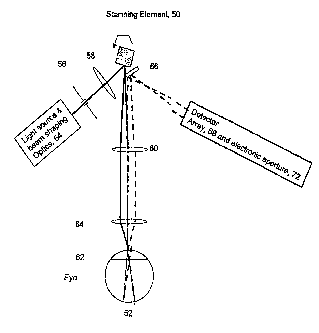
Fig. 3 illustrates an embodiment, which describes a group of configurations,
in which
a single scanning element 50 directs light from a light source and shaping
optics 54 to a target
14
CA 02653842 2008-11-27
WO 2007/142960 PCT/US2007/012726
52 but not the light remitted from the target 52. The light from an
illumination source 54
undergoes beam shaping and is brought to a focus in a plane conjugate with the
target 52 at a
slit aperture 56. According to one configuration, illumination from an
illumination source 54
utilizes beam shaping optics well known in the art that change illumination
from quasi-
Gaussian to a slit output. This change in illumination may be accomplished by
using a
cylindrical lens in the illumination pathway prior to the slit 56. However, if
edge emitting
illumination devices or other linear devices are used, a cylindrical lens may
prove
unnecessary. Slit aperture 56 is illustrated in more detail in Figs. 5-8, and
further described
below. As can be seen in Fig. 3 and Fig. 9, slit 56 has a long axis orthogonal
to the plane of
the figure.
In Fig. 3, the light passing through slit aperture 56 is directed by a
focusing element
58 onto the scanning element 50. The scanning element 50 rotates or oscillates
to reflect the
light sequentially across the target in a direction perpendicular to the long
axis of slit aperture
56. Throughout the figures, solid lines exiting the scanning element 50
indicate a scan path
for the illumination, and broken or dashed lines indicate detection pathways.
From the
scanning element 50, the light is then directed by one or more focusing
elements 60, through
a narrow angle of entrance, (e.g., the pupil) 62, to a focus at the target 52
(e.g., the retinal
plane). Fig. 3 illustrates the entrance and focal planes schematically only;
see Fig. 1 for
greater detail. The light at slit aperture 56 is in an optical plane conjugate
to the target 52.
The light at scanning element 50 is in an optical plane conjugate with the
plane of the narrow
angle of entrance 62. A focusing element 64 is preferably mounted for movement
in an axial
direction to allow focusing of the light on the target 52. When imaging a
target without a
lens (e.g. a target other than the human eye with a functional lens), focusing
element 64 is
optionally a set of lenses suitable for focusing on the target 52.
CA 02653842 2008-11-27
WO 2007/142960 PCT/US2007/012726
As noted above, scanning the light across the target through a slit aperture
(and
scanning again in the detection pathway if this is performed, described
further below) aids in
decreasing unwanted scattered light in the resulting image. The scanning can
be
accomplished in a variety of ways well-known in the art. For example, a mirror
component
may be mounted to a rotating or oscillating element, a magnetic device, a
spring, a torsion
rod, or other mechanically controlled device such as a solenoid, or a gravity
controlled
device. The scanning element can be activated in any suitable manner, such as
by a button or
lever press, a sliding switch, a toggle switch, or a knob rotation by the
operator. In one
embodiment, the scanning element is preferably driven by a battery operated DC
motor,
which is an inexpensive configuration and allows the device to be portable. In
one
embodiment, a rotating element that rotates in one direction, such as a DC
motor may be
used. Such a motor may be selected to be quiet in operation and operate with
little disruption
from environmental vibrating.
Light returning from the target 52 is separated from light striking the target
at beam
separation element 66. In the embodiment shown in Fig. 3, separation element
66 is
illustrated as a mirror that does not intersect the light directed towards the
target 52 on the
illumination pathway. The mirror is located on the return pathway to intersect
and thereby
reflect the light remitted from the target 52 on the detection pathway to a
detector array 68.
The separation element 66 may also comprise a beam splitter with the
reflective portion
intersecting the beam of light directed at the target 52, with the
transmissive portion directing
light remitted from the target, or any other combination of elements as
described concerning
Fig. 2 above to separate the light from the illumination pathway from that
remitted from the
target 52 and direct the remitted light towards the detection pathway.
Separation element 66
optionally contains additional mirror surfaces to direct the light in a
direction convenient with
16
CA 02653842 2008-11-27
WO 2007/142960 PCT/US2007/012726
respect to the configuration of the other components, thereby allowing
crowding of
components near the target 52 to be reduced. Further, additional mirror
surfaces may be used
and configured to reduce component crowding near mounting surfaces of focusing
elements
60 and 64, or to prevent components from interfering with the motion of either
focusing
element 64 or scanning element 50 by spatially separating the light directed
towards the
target 52 from the light returning from the target, unwanted, direct
reflections from focal
planes not in the plane of the target can be eliminated by minimizing the
spatial overlap at
beam separator 66. With respect to the target, the illumination is directed at
the target from a
slightly different position than is the detection pathway from the remitted
light so that there is
minimal spatial overlap between the detection and illumination pathways,
thereby
minimizing any unwanted reflections of optical elements, including those often
found in
association with the target such as the cornea and lens of the human eye when
the retina is the
target (see Fig. 1).
The separation element 66 may comprise a partially or fully reflective surface
that
does not intersect the light directed towards the target 52. The reflective
surface may
comprise a mirror or a beam splitter with the reflective portion not
intersecting the beam of
light directed at the target, as shown. The separation element can also be any
number of
other separation elements, such as a beam splitter with a reflective portion
intersecting the
beam of light directed towards target and a transmissive portion including a
mirror that
reflects less than 100% of the light towards the target or a transmissive
portion intersecting
the beam of light directed towards the target and the reflective portion
allowing the light from
the target to pass.
According to one embodiment of the present application, further decrease of
light
from unwanted planes can be obtained by directing the light on the detection
pathway from
17
CA 02653842 2008-11-27
WO 2007/142960 PCT/US2007/012726
the target 52 to a two-dimensional detector array 68 comprising a
complementary metal-
oxide-semiconductor chip ("CMOS") (referred to as a "CMOS detector array").
The CMOS
detector array operates in such a way that it acts as a "rolling shutter"
because an image is
formed by digitizing in an iterative line-by line fashion. Thus, as a beam of
light is directed
onto the CMOS detector array, only one small line or region of the image is
read or exposed
at any given time. Therefore, only light in phase with the particular line
being read or
exposed by the CMOS detector array is collected by the CMOS, thereby causing
the digital
image of the target to be "built" one line at a time. Optionally, if a more
advanced CMOS
detector can be used, allowing more than one line can be built simultaneously,
and providing
10, additional benefits and functionality discussed more thoroughly below. The
use of the
CMOS in lieu of a charge coupled device chip ("CCD chip") as used in previous
embodiments creates multiple unexpected benefits. While it was previously
thought that
synchronizing the rolling shutter feature of the CMOS detector array with the
scanning slit
aperture would be difficult, thereby increasing costs in production of the
device, it has been
found that use of the CMOS detector array itself acts as a confocal aperture
due to its rolling
shutter function, thereby eliminating the need for several expensive focusing
and other
elements that were necessary in the detection pathway in earlier embodiments.
In addition, it
was found that the use of the CMOS detector with a rolling shutter feature
significantly
reduces or eliminates blooming of an image, and further allows several
additional
functionalities to be present in the device that were not present in previous
embodiments.
According to another embodiment of the present application, an optional
electronic input
aperture is substituted or added to allow adjustment of the width of the slit
that is scanned, as
well as the width of the slit that is detected through the detection pathway.
18
CA 02653842 2008-11-27
WO 2007/142960 PCT/US2007/012726
In addition, the use of a CMOS detector array allows one to eliminate elements
between beam separator 66 and detector array 68. This allows for a complete
change of the
geometry of the device, because the rolling shutter feature reduces the need
for a third
scanning face and facets needed during the acquisition of each image. The
elimination of
these components allows for a reduction in optical aberrations that affect the
resultant image,
and further allow for an increased field size imaged by the device. For
example, the present
embodiment allows for a field of view 1.5 to 2 times wider than the twenty
degree (20 ) field
size of the previous embodiments without otherwise significantly altering the
design of the
device. A greater field of view of the device translates into a more user
friendly imaging
system, because an operator does not need to align the device with the eye as
exactly as he or
she would be required with a device that was more limited in field size.
Yet another functionality achieved through the use of a CMOS detector array
with a
rolling shutter feature is the ability to use scattered light imaging,
increased sampling in the
case of low signal, and image sharpening. For example, if the CMOS array is
read line by
line, it is possible to select a leading line or a lagging line in precise
alignment with the
optical axis of the illumination beam. When the illumination beam is digitally
imaged, using
the leading or lagging line or both together, a scattered image results. In
one embodiment,
two or more lines are digitally imaged in close succession to one another, or
even
simultaneously. Imaging these two or more lines allows for an overall image
with a more
precise image of a moving target, such as an eye, and allows reduction or
elimination of
shadowing from detection that is asymmetric. With non-moving targets, two
images are
acquired sequentially and then combined to provide a multiply scattered image
without the
use of advanced CMOS hardware. In addition, the input and detection apertures
can be
adjusted relative to each other to provide increased illumination control,
more or less
19
CA 02653842 2008-11-27
WO 2007/142960 PCT/US2007/012726
scattered light, and correction, of poor illumination or return at the edges
of the field. An
electronic shutter can operate with sufficient speed to alter the illumination
pathway within
each line of the image when necessary as discussed further below. Optionally,
more than one
line in the CMOS detector can be activated to allow the detection of more
light, with or
without the additional aperture.
Using the imaging method described above, one embodiment of the present
application allows for image sharpening when two or more lines adjacent to the
on-axis line
on the CMOS output are subtracted from the on axis line. Optionally, the two
lines may be
subtracted in a weighted manner. While it has been known in the art to use
image processing
with high contrast laser images to create such image sharpening, the image
processing has
always been done after the image was created. The present embodiment of the
device allows
the sharpening and image processing to occur while the target is being imaged,
thereby
allowing the operator to see the sharpened image at the time the target is in
front of him or
her. Therefore, since the sharpened image is able to be viewed by the operator
while taking
the image, the operator can determine whether additional images need to be
taken to ensure
that a quality image results.
According to yet another embodiment of the present application, a bi-
directional scan
is utilized, wherein multiple lines are detected and imaged sequentially (or
otherwise) in
differing directions. For example, a first scan sequentially detects and
images lines toward
the left of the starting position while a second scan sequentially detects and
images lines
toward the right of the starting position. Optionally, both the first and the
second scan occurs
simultaneously, and timing software is used to create multiply scattered light
images from
these scans.
CA 02653842 2008-11-27
WO 2007/142960 PCT/US2007/012726
Utilizing a CMOS detector array 68 to detect and build an image has the
additional
advantage over previous embodiments in that images obtained with a device
according to the
present application are optionally stored to memory media that is common-even
in the retail
consumer market. For example, experiments utilizing certain embodiments of the
present
application utilized flash memory cards and digital capture cards in a typical
personal
computer processor or digital camera. It will be appreciated that several
other conventional
or non-conventional storage media well known in the art may be used to acquire
images
detected by the CMOS detector array. Yet another advantage to using a CMOS
detector
array in lieu of a CCD chip is that the CCD vertical resolution is decreased
by a factor of 2 in
each field, because the CMOS detector array is not interlaced as is the case
with interlaced
CCD chips. Progressive scan chips do not have the reduction of vertical
resolution, and along
with CMOS chips are preferred when target motion such as eye movements are of
concern
because sequential scanning and similar schemes allow an image to be built up
with adjacent
structures sampled at more similar points in time, compared with interlaced
schemes that
acquire odd lines, and then even lines. Additionally, interlaced CCD chips
require a 30 Hz
frame rate, whereas CMOS chips operate at a lower sampling rate, thereby
allowing
improvement of signal to noise ratio. Further, use of a CMOS detector array
instead of a
CCD chip has resulted in reduction of-stray light from the several reflective
surfaces required
in the CCD embodiments, including those that allow the collection of light
before and after
the time period contributing to the image, with the CMOS embodiment thereby
increasing
detection of a higher proportion of light related to the target and improving
image quality
over sample and hold systems.
Returning now to Fig. 3, in cases in which a CMOS with a rolling shutter
serves as
the two dimensional ("2D") detector array 68, the reading of the data line-by-
line in a
21
CA 02653842 2008-11-27
WO 2007/142960 PCT/US2007/012726
sequential manner serves as an aperture 72 to limit the unwanted stray light.
Only the light
striking the line being read contributes to the image, which is in a manner
analogous to only
the light passing through a slit aperture reaching the target. As the CMOS
chip is in a plane
conjugate to the retinal plane, use of its inherent sampling scheme
constitutes a confocal
aperture, thereby reducing optical crosstalk spatially and increasing image
contrast.
In cases in which the 2D detector array 68 has a sample and hold or other
strategy that
does not include timed line-by-line sampling to limit the area sampled at a
given time, then a
separate electronic aperture may be introduced to serve as detection pathway
aperture 72
shown in Fig. 4. An LCD array that is pixel-by-pixel or line-by-line
addressable and changes
from transparent to opaque may be placed in close proximity so that the light
in the detection
pathway is limited spatially, and the area that is transparent corresponds to
that being
illuminated by the scan across the 2D array 68. As the scan progresses, the
transparent area
sweeps along in corresponding manner. However, this method requires another
element to
control for timing the sweeping action of the transparent area, unlike the
CMOS rolling
shutter method. According to one embodiment, a separation element 66 may be
used to
reduce pupil plane, or non-conjugate plane, reflections significantly. For
targets that are
stationary, or targets that can tolerate more light and thus could be scanned
with high
intensity and high speed, this objective may be removed.
For purposes of microscopy or fluorescence measurements in the eye, the
electronic
detection pathway 72 may optionally be made so narrow as to allow optical
sectioning or
wide enough to incorporate as much signal as possible, and may be configured
as to include
or exclude fluorescent barrier filters.
The rotation of scanning element 50 shown in Fig. 3 is in sufficient synchrony
to
allow line-by-line correlation of the illumination beam as it is scanned.
Therefore, the
22
CA 02653842 2008-11-27
WO 2007/142960 PCT/US2007/012726
position of the of aperture 72 is reasonably synchronized with scanning
element 50. This may
be accomplished either via open loop and calibration or closed loop methods
well known in
the art.
Figs. 4a and 4b further demonstrate a certain embodiment of the slit aperture
56
conjugate to the retinal plane in the illumination pathway and the electronic
aperture
conjugate to the retinal plane in the detection pathway. As shown in Fig. 4a,
at a first time,
light passes through slit 56, travels through the instrument, and the linear
beam of light 71 is
swept across the electronic aperture 72. As shown in Fig. 4b, at a second time
equal to the
first time plus an additional time, the linear beam of light 71 has moved to a
second position
on electronic aperture. Unwanted light from planes outside the target area, as
well as light
that has scattered across the target, is reduced by the use of aperture 72. As
stated above, the
rolling shutter function of the CMOS chip has this property inherent in its
operation.
Alternatively, according to another embodiment of the present application, a
mechanical,
electronic, or other shutter with a movable transparent area may be used in
close proximity to
the 2D detector array, allowing another 2D detector array such as a CCD, video
camera, or
other detector array to be used. The transparent area may be readily moved in
devices such as
LDC displays.
Figs. 5a and 5b illustrate that the width of slit 56 may be adjusted readily,
and in a
more rapid manner when it is electronic than when it is mechanical. As shown
in Fig. 5b, a
wider slit allows more light to enter the imaging system, thereby increasing
image intensity.
The relative widths of slit 56 and detection pathway 72 determine the sampled
region, and
increase or decrease the depth of field. Very narrow elements in slit 56 and
detection pathway
aperture 72 lead to a small volume of light sampled at the detector, and
therefore optical
sectioning and high contrast in the plane of focus, as shown in Fig. 5a. Wider
elements, such
23
CA 02653842 2008-11-27
WO 2007/142960 PCT/US2007/012726
as that depicted in Fig. 5b, allow a large volume of light to be sampled and a
larger depth of
field more readily useful in the moving eye. More scattered light is collected
in the
configuration shown in Fig. 5b, and this scattered light information can be
useful in revealing
structures not otherwise seen.
Fig 6. depicts a method for producing scattered light imaging with a
relatively wide
slit 56 in the illumination pathway made by any means that transmits light
such that a wider
area of the target is illuminated and the light returning is captured by a
confocal aperture in
the detection pathway 72 that is offset from the main illumination axis, shown
by the dashed
lines beneath detection pathway aperture 72. Detection pathway aperture 72
acts as an
1 o electronic aperture that is inherent in the CMOS shutter. Specifically,
detection pathway
aperture 72 acts as an electronic aperture by assigning a column on the chip
to actively obtain
image data that are advanced or delayed from the main illumination position on
the target.
The position(s) and width(s) are readily modified with ancillary electronic
apertures, but, in
the rolling shutter (line-by-line read out) on a CMOS chip, there must be on-
board processing
or post-processing to incorporate any functions other than a delay or advance
of image
capture via the synchronization. This method produces multiply scattered light
imaging, but
results in asymmetric illumination and detection, which can lead to shadows in
the image that
are difficult to distinguish from absorptive structures. Symmetric
illumination can be
obtained by combining two images, each having a displaced read-out from the
illumination,
2 o but in opposite directions from the illumination axis. This is not a
disadvantage with
nonmoving targets when relatively high light levels are used, and when two
images may be
taken is close succession. However, when moving targets are imaged, an
alternative
embodiment utilizes two detector arrays (such as CMOS detectors)
simultaneously, with
24
CA 02653842 2008-11-27
WO 2007/142960 PCT/US2007/012726
independent shutters, with one detector array allowed to lead the light
source, and the other
lagging behind.
Turning now to Fig. 7, according to yet another embodiment of the present
application, another method for producing scattered light imaging utilizes a
patterned input
illumination by introducing two or more transparent regions to the slit 56 in
the illumination
pathway and using the detection pathway aperture 72 as a confocal aperture. In
this example,
the central or on-axis portion of slit 56 is opaque and two transparent bars
flanking the central
portion of that slit. Light transmitted off axis is led through the instrument
to the target, and
the portion that returns on axis passes through the detection pathway aperture
72, which is on
axis. The on axis light returning from the target is largely scattered
multiple times off target
structures, and that light that is singly scattered from the illumination
pathway slits 56 is
blocked by the aperture. With an electronic aperture, this light arrives at
the wrong time to
pass through the aperture or be sampled by the rolling shutter action of CMOS
chip 68.
Fig. 8 illustrates sample combinations of slit 56 and aperture 72 with post
processing
to achieve confocal imaging, multiply scattered light imaging, and/or image
sharpening.
Processing may be accomplished by using either a detector array 68 with
onboard processing,
or digital or analog device(s) 42 for storage and comparison of the images,
thereby allowing
image comparison or computation. For example, as shown in Fig. 8, a multiply
scattered light
image is taken with the linear beam of light 71 taken at time A (referred to
as "line A"), and
linear beam of light 71 taken at time B (referred to as "line B"). Time A and
B may be the
same time, may be sequential, or may be at significant periods of time apart
from one
another. As an example, the scanning occurs progressively, with sampled lines
A and B, and,
illustratively there may be an additional line C (not shown), such that line B
is between line A
and line C on the detector array 68. By using the simple formula aB - b(A +
C), where a and
CA 02653842 2008-11-27
WO 2007/142960 PCT/US2007/012726
b are the weighting factors with variable sign and amplitude. To accomplish
highly flexible
confocal imaging, a is positive and b is negative and between 0 and 1, then a
portion of the
light received through A and C will be added to the light from B to form an
image, with A, B,
C, and any further lines together serving as a confocal aperture of adjustable
width and with
the possibility to capture a variable portion of the scattered light not
passing through B,
optimized according to imaging task. To accomplish image sharpening, if a is
positive and b
is positive but between 0 and 1, then this formula is used to subtract a
portion ranging from 0
to 100% of the amount of light in A + C, thereby removing the scattered light
from an image
based on B without further need for adjustment of slit 56, accomplishing
image. sharpening.
Optionally, this method may be generalized to more lines than A through C, and
additional
weighting factors, allowing the full flexibility needed for each imaging task.
For multiply
scattered light imaging, weighting factor a is negative or a factor less than
1, and b is
negative, so that more total weight is assigned to data passing through lines
A and C. Again,
additional lines, including those lines further removed from B, and
corresponding weighting
factors may be used to provide flexible imaging according to the target and
imaging task. For
weak multiply scattered light signals, proportionally more weight may be
needed to be given
to achieve an image.
The quality of the beam in imaging is important, and a slit can be formed by
using
only a cylindrical lens in beam shaping portion of element 54 and by slit 56
in Fig. 3, but
using both elements improves energy efficiency via element 54 and the slit 56
allows for
more precise sampling than does using only by element 54. Optionally, light at
the slit 56 is
in an optical plane conjugate to the plane of the target 52. Further,
optionally, the slit can be
generated by a transmissive or reflective spatial filter, as well as an
electronic one, such as a
26
CA 02653842 2008-11-27
WO 2007/142960 PCT/US2007/012726
spatial light modulator or LDC device, as described above. Additionally, the
beam quality
and slit may be optimized for a specific imaging task.
The position of the target plane is manipulated by the movable lenses or other
focusing elements, for instance lens 64 shown in Fig. 3. In one exemplary
embodiment, the
dimensions of the input pupil to the target 52 are small, no more than 2.5 mm
in diameter.
This permits use of the device in brightly illuminated surroundings or with
older people in a
remote setting. The size of the target to be imaged, when the human eye is the
target, is from
about 6 mm to about 12 mm, differing from highly magnified experimental
instruments, but
providing a field of view of about 200 to about 40 visual angle as in
conventional
ophthalmic cameras.
As the input and exit pupils are limited to a total of about 2 mm to about 2.5
mm, light
efficiency is a concern, particularly when the pupil is not dilated. According
to one
embodiment of the present application, scanning is done in one dimension
unlike the majority
of commercial devices, which scan in two dimensions. An improvement in signal
to noise
ratio can be achieved by reducing the speed of scanning. Unlike prior art
commercial devices,
which do not scan, an improvement in light efficiency may be obtained and an
improved
image quality is obtained by scanning.
A criterion in the design of a device according to the present application is
to preserve
a substantial amount of light, thereby allowing a maximum amount of light to
reach the
detector from the eye. Using such a criterion in design allows significantly
better imaging,
particularly since retinal imaging according to the present application is
often performed
through a pupil that is not dilated-thereby creating a condition that would be
considered to
be "light-starved" in other systems. In addition, the scanning device can
operate slowly near
the range of about 1 HZ to about 30 Hz, rather than the typical devices used
for retinal
27
CA 02653842 2008-11-27
WO 2007/142960 PCT/US2007/012726
imaging such as a continuously moving galvonometer or rotating device that
operates at
about 25 Hz to about 60 Hz. The lower frequency range also allows for less
power
consumption and a mechanically less sophisticated device to be used for
scanning. The slow
scan can be done such that, when the scanning device is activated by the
operator, the
scanning can be done with a single or limited number of sweeps across the
target.
While the foregoing describes several embodiments of a device according to the
present application, it will be appreciated that several other considerations
may be taken to
alter the application of the device, or to alter configurations of the device.
For example, in
another embodiment using a limited number of scans, reduced resolution is used
during one
or more frames to assist with light level, target positioning, and focusing
using faster data
acquisition, and then higher resolution is used for one or more good quality
still frames.
Many two dimensional arrays used in consumer electronics now permit operation
in more
than one mode. Similarly, detector arrays offer more than one resolution.
Thus, scanning and
acquisition speed, light level, and gain can be traded off against resolution,
as will be
appreciated by those skilled in the art.
It will be appreciated by those in the art that the small pupil size and small
device size
impose constraints on the field of view, which is most likely to be
approximately about 20
to about 40 with optical resolution that supports a digital resolution of
approximately 512
pixels x 512 pixels or 640 pixels x 480 pixels up to a I megapixel detector. A
large depth of
field is preferred for use with human patients, and the device may have
intentionally limited
confocal sectioning capabilities. A large depth of field reduces the need for
a large input
beam at the pupil, which allows for better axial resolution. Reduction of out
of focus light
minimizes artifact from anterior segment optics. An aperture in the plane
confocal to the
retinal plane is optionally used according to one aspect of the present
application. Further,
28
CA 02653842 2008-11-27
WO 2007/142960 PCT/US2007/012726
polarization optics are optionally used. Another way to provide sufficiently
long path lengths,
large depth of field, and good image quality is to use a telescoping frame or
further fold
mirrors. The path lengths can be extended by mirrors on or near the exterior
portions of the
frame that are moved, or on another movable component. Therefore, the present
device
according to the application avoids a disadvantage in many prior art designs-
having a high
f-number final lens in a position such that the pupil plane reflection is
sampled in the retinal
plane. Therefore, the present device does not produce images which result in a
bright,
unwanted reflection in the image of the retina.
In the -device according to the present application, the focusing mechanism is
optionally kept simple to minimize complexity of use, size, and weight.
Focusing may be
achieved by increasing or decreasing the relation of retinal and pupil planes
(the desired focal
plane and the entrance plane) by the use of one or more movable mirrors and/or
lenses, such
as shown in Fig. 3. These components may be operable by either mechanical or
electrical
control. In one embodiment, a movable lens or lens array is provided, as well
known in the
art. The moving mirror or lens can be operated manually by, for example, a
rotating knob
operated by a single finger or thumb, by grasping a rotatable lens housing, in
a manner
similar to a camera, by a slide switch, or any other mechanical positioning
device known in
the art. Optionally, the moving mirror or lens can be motorized, preferably
using a battery-
powered DC motor. Optionally, an AC motor can be used if there is a connection
to an
external AC power supply.
According to one aspect of the present application, proper focus can be found
through
visually inspecting images on a display; by using an indicator to locate the
brightest reflection
returning from the target (without necessarily having to provide visualization
of the data); or
by using lower resolution images, or a small number of images acquired more
rapidly, up to
29
CA 02653842 2008-11-27
WO 2007/142960 PCT/US2007/012726
video rate, to find the focus quickly, after which an image having a better
resolution is
provided. The focus can be a manual mechanism or an autofocus mechanism well
known in
the art. Finally, the focus can be determined based on all or a portion of the
image.
According to one aspect of the present application, the device may include a
display
on which the user can see the image, such as a liquid crystal display (LCD).
However,
because an onboard LCD adds weight, may be fragile, and draws current, it may
be desirable
in some embodiments to eliminate a display and provide only a focus indicator.
As noted
above, when the retina is in focus, this layer provides the greatest light
return throughout the
visible spectrum and near infrared. Therefore, according to one aspect of the
present
application, an image can be focused by positioning the image on the anterior
segment to
decrease this signal, and the focal plane to sample the retina adjusted to the
maximum
brightness. Thus, while an image is useful for focusing, with a large depth of
field, an
indicator may optionally be used. The indicator may be a display, a light when
a criterion is
reached, a light that gets brighter or dimmer corresponding to the amount of
light received, a
dial, a digital read-out panel, a sound, a needle display, or any other
element that can provide
a signal to the user that focus has been obtained.
The device may optionally include a display for viewing the image after its
acquisition. The display may be a liquid crystal display (LCD) or other
suitable display
device. The image data may be transferred by USB, IEEE 1394, a wireless
protocol, or other
connection to a device or computer, as is well known in the art. The device
may further
optionally include one or more onboard memory devices, either in the
integrated circuits or a
removable memory device or film that can be transferred to an external viewing
device such
as indicated at 44 in Fig. 2. The data may be transmitted by either wire or
wireless methods
to a receiving device, such as a computer, personal desk assistant, cell
phone, or other device.
CA 02653842 2008-11-27
WO 2007/142960 PCT/US2007/012726
According to yet another embodiment of the present application, to view
structures in
a plane not conjugate to the retina of the eye, modifications can optionally
be made by a
focusing assembly as shown by lenses 60 and 64 in Fig. 3. A further lens or
mirror assembly
may be added, existing lens or mirrors removed, or other lenses or mirrors
substituted for the
focusing assembly, as will be appreciated by one of ordinary skill in the art.
These structures
include the anterior segment of the eye, but are not limited to ocular
structures and could
include skin or any other biological or non-biological structure. The narrow
entrance pupil
and the separation of illumination and detection pathways distinguish this
design from an
optical confocal microscope device intended for optical sectioning with the
highest axial
resolution, although the embodiments shown in Figs. 3-8 allow for an
instrument with some
optical sectioning capability, i.e. an instrument that could be used as.a
microscope or general
purpose imaging device of modest resolution and rejection of out of plane
remitted light. The
focusing elements as shown can optionally be used to provide an image that
enlarges the
view of a target, and further enlargement of an image for viewing occurs
largely
electronically, thus broadening the potential uses beyond that of the human
retina or eye as a
whole. According to one aspect of the present application, the scanning of the
illumination
source with respect to the target provides an image of higher contrast than
does typical flood
illumination or illumination from existing and external sources such as
daylight, and in this
way broadens the potential uses of the device beyond the scope of the human
retina or eye.
According to one aspect of the present application, there are several
structures in the
anterior segment of the human eye that may be imaged by using ancillary or
substituted
focusing elements that are not in the focal range of the digital retinal
imaging device of the
present application. For example, the device according to the present
application could be
used to image corneal trauma or disease, results from corneal surgery or
refractive laser
31
CA 02653842 2008-11-27
WO 2007/142960 PCT/US2007/012726
surgery, a foreign body in or on the eye, a chemical injury or burn, iris
neovascularization,
exterior ocular injuries, bums, contact lens fit, external inflammation,
infectious disease, tear
duct problems, lid lesions, pterigeum, scleral or iris vessel problems, or
other data needed to
document the emergency or health status of a patient.
In addition, it should be noted that the device as described may be optionally
housed
in a casing. Further optionally, controls, such as an on-off switch and a
focusing control, may
be accessible through the casing. The casing may be rugged and lightweight and
encloses all
the optical and electronic components described above. In addition, a head or
chin rest can
be optionally provided, and may be configured to allow a patient to hold the
eye in a steady
manner in alignment with the device. The head or chin rest may be operable to
telescope to
form a readily packed and carried portable device. In another embodiment, the
head or chin
rest can be folded to form a compact footprint. A further embodiment has a
casing that is held
by the user in a manner similar to a consumer digital camera or video game. A
viewfinder
may be provided for locating the eye. A control on the casing can act as a
toggle switch for
off and on and for various modes or resolution of image acquisition.
A number of embodiments of the present device have been built and tested to
determine the feasibility of obtaining acceptable eye images safely and under
battery power
with the capability of transferring images to a remote source. A number of
embodiments were
tested using a model human eye, as known in the art. The model eye was used to
determine
that the device is able to operate and obtain an image using an acceptable
amount of light that
is consistent with eye safety. The relative amount of light in the model eye
has been
calibrated to the human eye and is known.
An embodiment similar to that described above in Figs. 2 and .3 was built and
tested
on a human eye, after obtaining required regulatory approval. Suitable images
of the retinal
32
CA 02653842 2008-11-27
WO 2007/142960 PCT/US2007/012726
plane of a human eye were obtained at an appropriate resolution, having good
contrast, and
with no strong reflections from the corneal planes. Features known to be
unique to the
particular human eye tested were recognizable.
This application is particularly applicable within the fields of
ophthalmology,
optometry, emergency services, military ocular screening, ocular screening in
any mass
situation, health care workers providing diagnoses at locations remote from
eye care
specialists, telemedicine, and eye examination by persons without specialty
eye care skills,
such as pediatricians, ER technicians, or family practitioners. A primary
application of the
device is for use by, for example, emergency personnel, when there is a
suspicion of trauma
to the eye. In such situations, it can be helpful to know if an individual
with a suspected eye
injury can be allowed merely to rest for a period of time or if, instead, the
patient requires
further emergency treatment. A further application is the remote or mass
screening for
potential eye disease by personnel who are not primarily specialists in the
eye, such as
pediatricians or family practitioners, and also including workers who have
minimal medical
experience and lack instrumentation or computer expertise. The device has a
minimum of
controls, which provides simplicity in operation, so that a high degree
of.training is not
required to operate the device.
In contrast to the present invention, current commercially available scanning
laser
ophthalmoscopes are too large and expensive for use as a portable device in
the field. Further,
these devices are complex and require a user to be highly trained both in
using the device and
in reading the resulting ophthalmic images. The striking image quality of the
large SLOs and
the sectioning capabilities of tomographic devices, which spoil the signal to
noise ratio, are
not needed in the present device.
33
CA 02653842 2008-11-27
WO 2007/142960 PCT/US2007/012726
In other embodiments of the present application, a device may utilize 3 or
more light
sources to illuminate the target with different wavelengths that will enhance
the visibility of
certain features. Imaging can optionally be performed with a device having
one, two, three,
or more such light sources, with each source differing to provide unique and
beneficial
properties, such as a different wavelength, increased power, or different
polarization
properties. Light sources can optionally be controlled by the control
electronics 46 (see Fig.
2), for example, to turn on and off, to operate in a steady state mode or a
flash mode, or to
control intensity of the light, as discussed further below. The light from
each illumination
source can optionally undergo beam shaping prior to being directed towards
additional
elements in the optical imaging system.
According to yet another embodiment of the present application, light from
illumination sources can be directed with turning mirrors, and then combined
into a single
beam with beam combining elements, in a manner known in the art, published by
the
inventor. See, e.g. Elsner et al, 1992. Such combining elements can be
reflective and
transmissive elements; can be dichroic mirrors to take advantage of the
wavelength
differences of the illumination sources; or they can reflect or transmit
according to
polarization properties of the illumination sources. According to one
embodiment, each of
the illumination sources is combined to the next by a pair of beam combining
elements. For
example, a first element, such as a mirror, steers the beams and a second
element combines
the two beams and further steers one or the other beam. The position of the
combining
elements can be configured to minimize the space taken by the device or light
efficiency,
rather than configured for ease of optical alignment.
According to one aspect of the present application, intensity of the light
from the
sources may be controlled in any suitable manner if desired, such as to
decrease the level
34
CA 02653842 2008-11-27
WO 2007/142960 PCT/US2007/012726
down from the FDA approved level for continuous viewing. The intensity of the
light can
also be controlled electronically, via neutral density filter or color filter,
mechanically, in
which case slit 56 in Fig. 3 represents an adjustable slit or iris diaphragm
that may be
controlled mechanically. The illumination control device may thus be operated
mechanically
or electronically, such as with a finger operated screw. The intensity of the
light can also be
increased or decreased with a polarizing element. Alternately, adjustment of
the intensity of
the illumination light uses electronic control from the control electronics,
such as that
depicted in Fig. 2, an ancillary detector or the output from the detector
array 68 in
communication with the light sources or the intensity control element to can
be used adjust
power, voltage, or current. A detector gain control can be used as well to
increase or
decrease contrast.
In an exemplary embodiment using three illumination sources, such as shown in
Fig.
4 of the prior patent family, illumination sources included a Helium-Neon
("HeNe") laser at
543 nm, a diode laser at 830 nm, and a vertical cavity surface emitting laser
("VCSEL") at
850 nm. Illumination sources such as Diode lasers and VCSELs can readily be
operated using
direct current and can thereby be operated by one or more batteries. Battery
operation allows
the optical imaging device to be portable and used in remote locations. By
using two or more
sources that differ in the amount of absorption of features of interest, such
as the blood in a
hemorrhage, it is possible to use image comparison as in Fig. 8 to enhance the
detection of
such features.
In this embodiment, the VCSEL is of unusually small size for an illumination
source
in an optical imaging instrument, as VCSELs are typically used in
communications and
optical computing, not optical imaging instruments. The footprint of the
device using this
source is thus more compact, and the weight is reduced compared to
conventional imaging
CA 02653842 2008-11-27
WO 2007/142960 PCT/US2007/012726
devices. The energy efficiency of the VCSEL, being unusually high, as well as
the
possibility of utilizing direct current such as from a battery, also assists
in reducing the
weight and footprint of the present imaging device. This diameter of the laser
element of a
VCSEL can be as small as 50 microns, plus the associated housing and beam
shaping
elements that are larger; the total package except for the power supply is
approximately the
size of a small integrated circuit or transistor in a can mount. In this
context, the VCSEL is
merely one more electronic component in the circuit. The high energy
efficiency permits the
output to be in the low mW range when using a single battery, such as a 9 V
battery plus
current limiting circuitry.
Diode laser illumination source is of an intermediate size and provides an
intermediate footprint and weight, and also supports the possibility of
battery operation and
remote use. Any infrared or near infrared source having an appropriate size,
energy
efficiency, power density, beam quality, and weight can be used as an
illumination source to
replace the sources described above. As sources with high coherence lead to
interference
artifacts in the slit that is scanned, these are less desirable unless these
unwanted artifacts can
be reduced so that there are not illumination differences along the length of
the scanned slit.
Superluminescent diodes are one type of source that can be used to provide low
coherence.
When the target is the human eye or other substance that remits near infrared
or
infrared light, the target can be viewed with a safe and (where applicable)
comfortable
amount of illumination, using illumination sources either a laser diode or a
VCSEL. A near
infrared source is important for penetrating thin blood layers and the lens
with cataractous
changes. Near infrared sources, when used to image the retina, do not lead to
constriction of
the human pupil, thereby providing sufficient illumination to use the imaging
device in a non-
mydriatic manner, with either flashed or steady-state illumination. An
illumination source
36
CA 02653842 2008-11-27
WO 2007/142960 PCT/US2007/012726
with near-infrared wavelength having a beam of acceptable quality produces an
image of
acceptable quality when used in a scanning system, such as those depicted in
Figs. 2 and 3.
The imaging device can be limited to use with a near infrared source for use
in an
environment of daylight, room light, or other visible wavelength light by
positioning a filter
blocking the visible wavelength light, using any suitable position, where the
light is
approximately in a plane optically conjugate with the plane of target 52 of
Fig. 3, such as
between the target 52 and a focusing lens 64 in Fig. 3.
According to one embodiment, the illumination source 54, as depicted in Fig.
3, can
be of a shorter wavelength than sources in the near IR range. Examples
include, but are not
limited to, HeNe lasers, wavelength sources such as lamps and light emitting
diodes of
sufficient power density and beam quality to permit scanning of a slit of
uniform intensity
across the target, as would be known by those of skill in the art. In the eye
and other
biological tissues, the use of a shorter wavelength, specifically in the range
of 514 to 594 nm,
enhances the contrast of structures containing blood, but can lead to
constriction of the
human pupil. However, it was recently found that with sufficient contrast,
these features are
visible in near infrared light, possibly to a greater extent than that needed
for screening for
disease. For the detection pathway to utilize a modest cost detector array, it
is necessary to
use a sufficiently bright source to provide an image despite this
constriction. However, a
light source of short wavelength can be used in a flashed mode, following
alignment of the
target and the imaging device using a near infrared illumination source. An
example in the
human eye is the detection or management of diabetic retinopathy. Similarly,
for reflectance
or fluorescence imaging, a light source of one wavelength range can be used
for alignment
prior to imaging to prevent excessive light exposure, thermal changes, or
photobleaching. In
37
CA 02653842 2008-11-27
WO 2007/142960 PCT/US2007/012726
the eye three examples are fluorescein angiography and fluorophotometry in the
retina and
vitreous, and fluorescein staining for assessment of tear film quality for the
anterior segment.
In one embodiment, a laser scanning digital camera device features the ability
to scan
one or more light sources. Further each light source is specifically designed
for detection of
target characteristics according to a specific configuration of wavelength,
beam shaping,
illumination aperture, spatial or temporal modulation of the beam,
polarization content, or
structured illumination. By way of nonlimiting example, if scanning with a
slit, structuring
the illumination with a square aperture is optionally used to provide even
illumination across
the image. When even illumination is provided, target detection at any
location within the
field of view is possible.
According to one embodiment of the present application, the electronic
aperture is
synchronized in a closed loop manner with the active period of the detector.
This loop may
be closed by prior calibration, in situ calibration, or while operating the
device. The
synchronization may be determined by a master signal, the scanning element, or
the detector.
In one embodiment, the master signal may be generated by a read-out of the
position of the
scanning element. The position signal may be generated when the light from the
moving
scanning element reaches a detector, and this signal can indicate the
beginning of the image
or the position within the image for even more precise control, with the
detection of light
returning from the target synchronized with respect to the position on the
target of the
illumination. This allows the device to obtain images while using
exceptionally low cost
optical elements that serve as mirrors in the scanning element, since the
scanning slit overfills
the target pathway in the direction perpendicular to the scan and the timing
in the direction of
the scan is variable in a rapid and accurate manner. Synchronization of the
scanning element
38
CA 02653842 2008-11-27
WO 2007/142960 PCT/US2007/012726
to the target that is performed on portions of the image provides rapid
flexibility of aperture
position.
According to another embodiment of the present application, the digital image
device
is operable to provide a high quality image by using a series of images
acquired in succession
rapid enough to allow the adjustment of position of the target and instrument
with respect to
each other. In addition, according to certain embodiments, the images are
assessed for
quality and improved by the adjustment of parameters used in image
acquisition. The
adjustment is made more readily when the series of images is acquired in rapid
succession.
The adjustment is made by software, electronic circuitry, or the operator, or
a combination
thereof. Optionally, the digital imaging device is further capable of
providing onboard or
embedded control of parameters. The same control mechanism is optionally in
communication with electronic circuitry or a computer with sufficient memory
to allow
storage of images so that selection of the highest quality images can be
performed
immediately after acquisition. In a moving target such as an eye, or one that
is changing over
time, this provides a greater probability that an image of acceptable quality
is obtained. In
the embodiment with a unskilled user, the acquisition of images can be
adjusted to
incorporate sufficient time and number of images, and requiring little action
on the part of the
user, to improve the chance of acquiring suitable images. The control
mechanism can have
the capability of processing aspects of the image to assure quality control.
The control
mechanism is optionally capable of performing processing on the images and
then displaying
and storing these images.
According to one embodiment of the present application, the digital imaging
device is
operable to provide high contrast of features that may be used to identify a
target or portions
of the target that allow improved detection of the target itself, particularly
in the case of a
39
CA 02653842 2008-11-27
WO 2007/142960 PCT/US2007/012726
moving or changing target, or regions of interest within the target. In the
embodiment, a
wider field of view for imaging the retina is possible, and more precise
localization of the
regions within the retina becomes possible because two main features, such as
the fovea and
the optic nerve head, are now potentially within the field of view with
sufficient spacing that
localization is improved over identifying a single feature that is used in
current high rate
retinal tracking devices with and without polarization. In the embodiment with
polarized light
illumination, there is the potential for using the macular birefringence and
the optic nerve
head birefringence to identify two points within the retinal image of
sufficient spacing to
localize retinal features. The use of the electronic aperture further improves
the detection of
the macular and the optic nerve head birefringence by rejecting unwanted
scattered light that
does not contain polarized light information, but allowing sufficient light to
be detected to
provide a robust signal.
In the embodiment with reflected light illumination, there is the potential
for using the
macular and the optic nerve head features to identify two points within the
retinal image of
sufficient spacing to localize retinal features. The use of the electronic
aperture further
improves the detection of the macular and the optic nerve head features with
sufficient
contrast by rejecting unwanted scattered light that reduces image contrast,
but allowing
sufficient light to be detected to provide a robust signal.
In the embodiment with polarized light illumination, there is the potential
for using
the macular birefringence and the optic nerve head birefringence to identify
two points within
the retinal image of sufficient spacing to localize retinal features. The use
of the electronic
CA 02653842 2008-11-27
WO 2007/142960 PCT/US2007/012726
aperture further improves the detection of the macular and the optic nerve
head birefringence
by rejecting unwanted scattered light that does not contain polarized light
information, but
allowing sufficient light to be detected to provide a robust signal.
According to another embodiment of the present application, one or more
optical
channels can added to the digital device to provide images using illumination
differing in
wavelength, beam shaping, illumination aperture, spatial or temporal
modulation of the beam,
polarization content, or structured illumination. The additional optical
channels provide the
possibility of viewing with the wider field and low cost digital device, with
a flexible
electronic aperture, and simultaneously providing an image with different
information
content or providing a visual stimulus or alignment beam. In one embodiment,
the visual
stimulus is used to direct the position of the retina. Additionally, the
stimulus is optionally
used to elicit a response for diagnostic or experimental use with humans or in
situ use in
biological preparation. In one embodiment, the wide field with the scanned
slit illumination
is of sufficiently long near infrared wavelength, low power, and low duty
cycle to be
rendered nearly invisible to the human eye. Such conditions do not interfere
with a visual
stimulus or lead to heating in the retina or a biological preparation, but
provide localization of
the stimulus or illumination impinging on a preparation.
Fig. 9 illustrates an embodiment, which describes a group of configurations,
in which
a single scanning element 50 directs light from one or more light sources and
shaping optics
54 to a target 14 but not the light remitted from the target 14. The light
from an illumination
source 154 undergoes beam shaping by lens 155 and passes through square
aperture 156 to
ensure even illumination in one dimension when passing through cylindrical
lens 157 and a
slit aperture 56 , conjugate with the target 14. These elements 154, 155, 156,
and 157
together correspond to element 54 in Fig. 2. According to one configuration,
illumination
41
CA 02653842 2008-11-27
WO 2007/142960 PCT/US2007/012726
from an illumination source 54 utilizes beam shaping optics well known in the
art that change
illumination from quasi-Gaussian to a slit output. This change in illumination
may be
accomplished by using a cylindrical lens in the illumination pathway prior to
the slit 56.
However, if edge emitting illumination devices or other linear devices are
used, a cylindrical
lens may prove unnecessary. Slit aperture 56 is illustrated in more detail in
Figs. 5-8, and as
described above. As can be seen in the figures, slit 56 has a long axis
orthogonal to the plane
of the figure.
In Fig. 9, the light passing through slit aperture 56 is directed by a
focusing element
58 onto the scanning element 50. The scanning element 50 rotates or oscillates
to reflect the
light sequentially across the target in a direction perpendicular to the long
axis of slit aperture
56. Throughout the figures, lines exiting the scanning element 50 indicate an
illumination
path. From the scanning element 50, the light is then directed by one or more
focusing
elements 60, here shown as a movable lens 164 to focus the light through a
narrow angle of
entrance, (e.g., the pupil) 62 in Fig. 3. The light is further focused by
focusing elements 161
and 162, corresponding to 64 in Fig. 3, and bright the light to a focus at the
target 14 (e.g.,
the retinal plane). Fig. 9 illustrates the entrance and focal planes
schematically only; see
Fig. 1 for greater detail. The light at slit aperture 56 is in an optical
plane conjugate to the
target 14. The light at scanning element 50 is in an optical plane conjugate
with the plane of
the narrow angle, just anterior to the lens 24, shown in Fig. 3 as a narrow
angle of entrance
62. A focusing element 164 is preferably mounted for movement in an axial
direction to
allow focusing of the light on the target 14. When imaging a target without a
lens (e.g. a
target other than the human eye with a functional lens), focusing element 164
is optionally a
set of lenses suitable for focusing on the target 14, along with additional
lenses 161 and 162.
The wide field of view illustrated in Fig. 9 is improved by the use optical
design specialized
42
CA 02653842 2008-11-27
WO 2007/142960 PCT/US2007/012726
for wide field, illustrated here as a Kellner type of ocular mounted near the
eye, formed by
optical elements 161 and 162, or the use of an ophthalmic-lens that is
aspherical. In addition,
the wide field of view requires sufficiently large diameter lenses or mirrors
to allow a free
zone that passes the weak signal returning from the human eye, in particular
focusing element
164.
As noted above, scanning the light across the target 14 through a slit
aperture (and
scanning again in the detection pathway if this is performed, described
further below) aids in
decreasing unwanted scattered light in the resulting image. The scanning can
be
accomplished in a variety of ways well-known in the art in addition to the
method in Fig. 9.
In the optical pathway between scanning element 50 contains one or more
separation
elements 66, 266, and 366, to direct additional optical pathways in or out of
the main
pathway. Separation element 66 in Fig. 9 corresponds to separation element 66
in Fig. 3, and
may consist of various reflecting or transmitting configurations. Separation
element 266
introduces a second optical channel of illumination. An illumination source
254 and its beam
shaping optics 255 may differ in wavelength, power, spatial or temporal
properties, beam
shape, focus, polarization characteristics or any of a number of other
properties. Light from
illumination source 254 is focused by focusing element 255 and directed
towards a target by
separation element 266, passing through focusing elements 164, 162, and 161.
Light from illumination sources 354 is directed towards the target, starting
from a
position outside the main optical pathway, shown here as directed towards the
anterior
segment of the eye and not towards target 14.
Light returning from the target 14 is separated from light striking the target
at
separation element 66. In the embodiment shown in Fig. 9, separation element
66 is
illustrated as a mirror that does not alter the course of the light directed
towards the target 14
43
CA 02653842 2008-11-27
WO 2007/142960 PCT/US2007/012726
on the illumination pathway, but instead directs the light returning from
target 14 into a
detection pathway, illustrated as solid and darker gray lines. The light
remitted from the
target 14 in the detection pathway is focused by a focusing element 74 and
directed to a
detector array 68. The focusing element shown here is a mass produced and
inexpensive
camera lens, a double Gauss, but for our monochromatic images a lens of less
complexity is
also suitable. The detector array 68 is conjugate to the plane of the target
14. As in Fig. 3, a
wide range of combinations of separation elements 66 also comprise a beam
splitter with the
reflective portion intersecting the beam of light directed at the target 14,
with the transmissive
portion directing light remitted from the target, or any other combination of
elements as
described concerning Fig. 2 above to separate the light from the illumination
pathway from
that remitted from the target 14 and direct the remitted light towards the
detection pathway.
Separation element 66 optionally contains additional mirror surfaces to direct
the light in a
direction convenient with respect to the configuration of the other
components, thereby
allowing crowding of components near the target 14 to be reduced. Further,
additional mirror
surfaces may be used and configured to reduce component crowding near mounting
surfaces
of focusing elements 160, 161, and 164, or to prevent components from
interfering with the
motion of either focusing element 164 or scanning element 50 by spatially
separating the
light directed towards the target 14 from the light returning from the target,
unwanted, direct
reflections from focal planes not in the plane of the target can be eliminated
by minimizing
the spatial overlap at beam separator 66. With respect to the target, the
illumination is
directed at the target from a slightly different position than is the
detection pathway from the
remitted light so that there is minimal spatial overlap between the detection
and illumination
pathways, thereby minimizing any unwanted reflections of optical elements,
including those
44
CA 02653842 2008-11-27
WO 2007/142960 PCT/US2007/012726
often found in association with the target such as the cornea and lens of the
human eye when
the retina is the target (see Fig. 1).
The separation element 66 may comprise a partially or fully reflective surface
that
does not intersect the light directed towards the target 14. The reflective
surface may
comprise a mirror or a beam splitter with the reflective portion not
intersecting the beam of
light directed at the target, as shown. The separation element can also be any
number of
other separation elements, such as a beam splitter with a reflective portion
intersecting the
beam of light directed towards target and a transmissive portion including a
mirror that
reflects less than 100% of the light towards the target or a transmissive
portion intersecting
the beam of light directed towards the target and the reflective portion
allowing the light from
the target to pass.
According to one embodiment of the present application, further decrease of
light
from unwanted planes can be obtained by directing the light on the detection
pathway from
the target 14 to one or more two-dimensional detector arrays 68 comprising a
complementary
metal-oxide-semiconductor chip ("CMOS" or "CMOS detector array"). The detector
array
68 is in synchrony with the illumination timing and of a suitable sensitivity
at the wavelength
or wavelengths of light returning from the target to allow detection of light
returning from the
target. The detector array 68 may detect light returning from the target from
illumination
source 154 or 254. A similar detector array 368 detects the light that is
returned from a
target, such as the ocular lens 24 or pupil 16, directed by separator element
366, and focused
by focusing element 374 onto detector 368.
The combination of illumination sources and beam shaping optics shown in Fig.
9
may be incorporated with further devices such as polarization generation
devices, temporal or
spatial filters, and position manipulators to use the scanning engine and
flexible electronic
CA 02653842 2008-11-27
WO 2007/142960 PCT/US2007/012726
aperture to build imaging devices for not only reflected and multiply
scattered light, but also
structured illumination for enhanced detection of targets and stereogrammetry,
polarimetry,
fluorescence imaging, and stereo imaging.
A target image provides a variety of features, and to localize these better
than
methods using rotation or translation about a single point, two references may
be used. The
macula and the optic nerve head are two such major features that can be used
to localize or
stabilize features in the retina, for the birefringence signal radiating from
the macula and the
birefringence signal from the nerve fiber bundles radiating from the optic
nerve head.
The illumination striking the target may be patterned, and a pattern such as
stripes
provides a convenient method for generating the pattern. Illumination sources,
such as those
shown as 154 or 254 in Figure 9, can be temporally modulated to produce
stripes as they
sweep across the target 14. Use of a Vertical Cavity Surface Emitting Laser as
an
illumination source provides the capability for rapid modulation without
additional wear and
tear, as do Light Emitting Diodes and other modulatable sources or sources
fitted with
15' temporal modulating devices such as choppers or shutters.
When operating the LSDC in closed loop mode, the scanning element 50 in Figs.
2
and 9 can be operated as either the master or the slave. One method of
synchronization, is to
use the a motor encoder on scanning element 50 in Figs. 2 and 9. The encoder
can be used
either as a signal to provide a master signal for synchronization or as a
signal to provide
improved scanning element 50 positioning and rate.
In one embodiment of synchronization of the image acquisition by detector
array 68
to the scanning element 50, the scanning element 50 serves as the master, and
the detector
array 68 synchronized to it by means of a Start of Scan with a fixed point,
ancillary detector.
In a point scanning system, a Start of Scan is typically used for
synchronization in one
46
CA 02653842 2008-11-27
WO 2007/142960 PCT/US2007/012726
direction, but must be further synchronized with the scanning element in the
orthogonal
direction, and does not readily offer the possibility of lessening the
tolerances on the position
and timing of the components in a unitary scanning element 50. In a slit
scanning system,
such as that shown in Figs. 2 and 9, this allows lower cost in an obvious
manner. The start of
scan also permits timing out the illumination source 154 or 254 for safety and
power
efficiency. In one embodiment, the start of a scan has a series of components
and signals,
with the scanning element consisting of a polygon mirror on a DC motor,
serving as the
master for the synchronization. The detector can be a pin diode, or other
detector, placed at
the edge of the retina plane A digital trigger signal may optionally formed. A
delay may also
added, which can be made adjustable by means such as a potentiometer, to allow
for variable
offset of the illumination reaching the position of the diode. This allows
adjustment of image
acquisition to be in synchrony with the illumination slit, or to be offset to
provide multiply
scattered light imaging. A start of scan signal can be formed, which can be
TTL, and the start
of scan signal is sent to the sensors.
In one alternative method of synchronization of the scanning element 50 in
Figs. 2
and 9 as the master, a detector array, such as a two dimensional CMOS detector
can be used,
rather than a single point detector. The position of the CMOS detector is
adjacent to the
retinal plane, with the advantage that the alignment to the detector array
used in imaging is
straightforward, and potentially of lower cost than adding an additional
circuit. The frame
rate of this synchronization method can be made very high, an advantage in
that the
synchronization can be made more precise. The gain of the detector array, such
as when
using a CMOS detector, is readily controllable, unlike the typical Start of
Scan with the fixed
point detector. The arrival of the illumination slit is detected at the
leading edge of the image
and then checked to maintain it within the appropriate region of interest,
mandated by the
47
CA 02653842 2008-11-27
WO 2007/142960 PCT/US2007/012726
position to be acquired by the electronic aperture. A Start of Scan signal is
determined from
the predicted arrival of illumination at the leading edge of the image, then a
line trigger is
generated for image acquisition at the appropriate time for each line or group
of lines on the
detector array.
The description above pertains to several illustrative embodiments of the
invention.
Many variations of the invention may be envisioned by one skilled in the art.
Accordingly,
such variations and improvements are intended to fall within the compass of
this disclosure.
The invention is not to be limited by what has been particularly shown and
described, except
as indicated by the appended claims. The aim of exceptionally low cost, low
power
requirements, smaller size, and ease of use can be applied beyond the use in
the eye field.
For instance, it will be appreciated that embodiments of the present
application can be used as
a general imaging instrument, a microscope, or an endoscope. The embodiments
for eye
applications include diabetic retinopathy, age-related macular degeneration,
macular hole,
epiretinal membrane, glaucoma, contact lens problems, ocular inflammation,
infectious
diseases, ocular trauma, and other conditions. An all-in-one device with
increased ease of use
that allows simultaneous or nearly simultaneous images of both the anterior
segment and
posterior segment of the eye that are readily viewed, stored, or transmitted
would be greatly
appreciated.
Further, embodiments of the present application can also be used as a general
imaging
2o device, or for microscopy, to improve image detection of targets and
potentially decrease the
light level needed for image formation. When used with a scanning element,
certain of the
above embodiments efficiently use light and decrease the potential for
unwanted scattered
light. For the purpose of developing imaging applications, it is not often
known with certainty
how much light will be collected from the target and the characteristics of
that light. The
48
CA 02653842 2008-11-27
WO 2007/142960 PCT/US2007/012726
electronic aperture capability, in an optical plane conjugate to the target
plane, helps control
the sampling of light. The aperture allows the detection of reflected or
multiply scattered
light to varying degrees in a rapid manner and without mechanical parts.
Similarly, the
electronic aperture can be rapidly adjusted to emphasize contrast, such as by
reducing the
aperture size to detect mainly reflected light, or increase signal-to-noise
ratio, such as by
increasing aperture size to obtain more total light. Thus, the electronic
aperture provides
more flexibility in sampling the light, which allows an optimal setting to be
determined for a
naive user for each application. A user or instrument developer can select the
setting in an
unusually flexible and rapid manner, according to the needs of each
application. One such
use is in the field of infectious disease, in which dark field imaging has
already been shown
to be advantageous for the detection of malaria because it allows unstained
blood to be tested
(Jamjoom GA. Dark-field microscopy for detection of malaria in unstained blood
films. J
Clin Microbiol. 1983 May;17(5):717-21.) The use of an embodiment of the
present
application optimized to take dark field imaging has the advantage of less
handling of blood
or other substances that may pose additional health and safety issues, as well
as requiring less
expertise and equipment in slide preparation. A device that detects important
targets such as
blood-borne diseases requiring less expertise and cost would be greatly
appreciated.
Further, additional embodiments include optimizing the illumination light to
detect a
target for use with the electronic aperture. This optimization may take place
in the selection
of wavelength, beam shaping, illumination aperture, spatial or temporal
modulation of the
beam, polarization content, or structured illumination. This allows use for a
broad range of
applications and rapid, less expensive prototyping for applications. Such a
low cost device
that is flexible and easy to use, and far lower in cost than producing and
aligning a series of
mechanical apertures, and can be optimized readily according to the
application and the
49
CA 02653842 2008-11-27
WO 2007/142960 PCT/US2007/012726
illumination source, and has equivalent or improved detection of a target,
would be greatly
appreciated.
Yet another embodiment of the present application includes having more than
one
pathway for detection of light, each of which can utilize the electronic
aperture. The
additional detection pathways can differ in plane of focus, angle of incidence
or regard,
wavelength detection or filtering, sensitivity or gain, temporal or spatial
properties,
resolution, or polarization properties. Additional detection pathways allow
optimization at
reduced cost in instrumentation such as an all-in-one device for anterior and
posterior
segment of the eye, simultaneous confocal fluorescence and reflectance
imaging, confocal
multispectral imaging, stereo in the plane of choice, simultaneous detection
of reflected and
multiply scattered light, polarization imaging, and imaging techniques that
require synchrony
with target excitation or two or more detection channels. Such a device allows
a more
flexible means for providing near simultaneous observation of directly
backscattered and
multiply backscattered light than described in US patent 6,236,877 and related
work. As
such, a low cost device that is flexible and easy to use, or that can be
optimized readily
according to the application, and has equivalent or improved detection of a
target due to the
use of two or more detection pathways would be greatly appreciated.