Note: Descriptions are shown in the official language in which they were submitted.
CA 02654209 2012-04-05
Method, System, and Apparatus For Controlling An Electric Motor
Inventor: George I. Boyadjieff
John J. Hurst
Field
The present invention relates generally to appliances and equipment utilizing
an electrical
13 motor, and is more particularly related to methods, systems, and apparatus
for controlling an
electric motor for the conservation of energy.
Background
Power factor measures the ratio of average power to the apparent power in an
electrical
load. Power factor ranges from a value of 0 (where the impedance of the load
is purely reactive)
to 1 (for a purely resistive load). In practice, the power factor of
electrical devices ranges
somewhere between 0 and 1, and the closer this value is to unity, the more
efficiently energy is
consumed by the device and the less power is wasted. Therefore, for consumers
of electricity
that employ highly reactive loads (e.g. electrical induction motors), it is
desirable that steps be
taken to adjust the power factor of their apparent load to improve performance
and avoid wasting
1
CA 02654209 2012-04-05
enormous amounts of power. For example, a mill that consumes 100kW from a 220-
V line with
a power factor of 0.85 will require 118kW of apparent power supplied. But if
the power factor is
improved to 0.95, the apparent power supplied drops to 105.3kW. Many utility
companies
require such consumers to take affirmative steps to adjust power factor.
Large factories are not the only environments to benefit from improvement in
power
factor. AC motors are present in many different electrical appliances and
equipment from
compressors to elevators, and since they are usually inductive in their input
impedance, they
often present a less than desirable power factor rating, especially under
light load conditions or
during certain periods of load variance. To improve the power factor in AC
motors, controllers
to have been developed and are generally known in the art. Examples include
U.S. Patent No.
4,459,528, entitled "Phase Detector for Three-Phase Power Factor Controller"
(Nola '528); U.S.
Patent No. 4,266,177, entitled "Power Factor Control System for AC Induction
Motors"
(Nola '177); and U.S. Patent No. 5,821,726, entitled "Balanced and
Synchronized Phase
Detector for an AC Induction Motor Controller" (Anderson),
In general, the power factor mitigation approach taken by many AC motor
controllers is
accomplished by sensing the phase difference between the current and voltage
phasors and then
using a controller to adjust the actuation of thyristors in each AC motor
phase to attempt to
reduce the voltage and current phase lag. In an ideal implementation, if the
phase between the
current and voltage phasors can be brought to zero, the load looks resistive
to the power supply,
and therefore, the power factor would approach unity. While unity power factor
is not entirely
practically achievable, small improvements in power factor can make
substantial differences in
power consumption.
Many different approaches to improving power factor in electrical motors have
been
15 developed over the years. For instance, U.S. Patent No. 4,052,648 (entitled
"Power Factor
2
CA 02654209 2012-04-05
Control System for AC Induction Motors" (Nola '648)) describes a power
reduction system for
less than fully loaded induction motors. The phase
angle between current and voltage (motor power factor) is controlled. In the
Nola '648 system,
the motor power factor is controlled as a function of the difference between a
commanded power
factor signal and the operating power factor through control of thyristors
connected to the motor.
U.S. Patent No. 4,266,177, entitled "Power Factor Control System for AC
Induction
Motors" (Nola '177), is a system adapted to respond to conditions where motor
loads are
abruptly changed (e.g., by increasing the speed of full motor voltage turn-
on). In the Nola '177
system, a phase comparison is made by combining the voltage and current
derived square wave
signals and generating a series of pulses equal in time width to the phase
angle between motor
current and voltage. The variable width of the pulse is changed to a variable-
amplitude DC
signal whose amplitude is proportional to the phase difference. The phase
difference signal is
compared with a command voltage signal representing a desired minimum power
factor of
operation. The resulting difference signal, a circuit error signal, is then
used to control the on
time of a triac in series with the winding of the induction motor to maintain
motor operation at
the selected power factor. This has the effect of significantly reducing the
power input to a less
than fully loaded motor.
Inherent in changing these pulses into a DC signal is the necessity to filter
the pulses to
produce a smooth DC signal. This is accomplished, for instance, by using an
analog integrator.
Analog integrators, by their very nature, can create a time lag between the
actual change in phase
angle and the change the controller sees. This lag can be quite significant
compared to the
motor's ability to respond to a change in load. As a result, designs such as
those shown in U.S.
Patent No. 4,266,177 may require additional circuitry to cancel this time lag
during periods
where the motor's load suddenly increases.
3
CA 02654209 2008-12-02
WO 2007/143570 PCT/US2007/070250
U.S. Patent No. 5,821,726 addresses the response to large increases in motor
load. The
speed of response to a change from lightly loaded to fully load conditions
could be inadequate to
prevent motor stalling or vibrations, especially when the minimum power factor
command
setting is relatively high. For example, although the Nola system(s) responded
fairly quickly,
further improvements could be made to respond to large abrupt load changes
such as those in oil
well pumps, motor generator sets, stamping machines, refrigerator compressors,
and the like.
The filtering of the pulse train to create a smooth DC signal can compromise
the response
of the controller. High efficiency motors connected to controllers may also
enter into
undesirable periods of excessive vibration due to the controller's inability
to respond to these
high efficiency motors.
It would be desirable to provide a fast responding controller that has the
capability to
improve the control of the phase lag in induction motors and hence the amount
of energy saved.
It would also be desirable to provide a controller that is capable of working
with a broad variety
of electrical appliances that contain induction motors thereby improving power
factor and start-
up characteristics. It would also be desirable to provide a power factor
improving controller that
is programmable and may be customized to particular loads and operating
conditions.
Summary
The present invention provides systems and methods for control of a motor. A
phase
detector is coupled to a power supply. The output of the phase detector is
synchronized to a zero
crossing of a motor current of the motor and a zero crossing of the line
voltage. A digital
microprocessor coupled between the output of the phase detector and a
rectifier driver senses a
first time at which a phase of the motor voltage is crossing zero volts and a
second time at which
a phase of the motor current is crossing zero current. The digital
microprocessor determines the
difference in time between the first and second times and uses the difference
in time to calculate
4
CA 02654209 2012-04-05
a phase lag of the motor. The digital microprocessor uses the phase lag to
calculate a firing time of a rectifier to
command power efficiently to the motor.
In one aspect, the present invention resides in a system, comprising: a power
supply; a phase detector coupled
to the power supply, said phase detector having a first phase detector output,
said first phase detector output
being synchronized to a zero crossing of a motor current; and a second phase
detector output; said second
phase detector output being synchronized to a zero crossing of a line voltage
of said power supply; a rectifier;
and a digital microprocessor connected to the first and second phase detector
outputs and the rectifier; said
digital microprocessor sensing a first time at which a phase of the line
voltage crosses zero; sensing a second
time at which a phase of the motor current crosses zero; calculating a
difference between the first and second
times; calculating a phase lag of the motor based on said difference; and
calculating a firing time of the
rectifier based on said phase lag.
In another aspect, the present invention resides in a system, comprising: a
power supply;
a phase detector coupled to said power supply, the phase detector having a
first phase detector input coupled to
a first non-inverting input of a first operational amplifier via a second
voltage divider and a second inverting
input of a second operational amplifier via a third voltage divider, a second
phase detector input coupled to the
first inverting input of the first operational amplifier via a first voltage
divider, and a phase detector output that
includes an output of the first operational amplifier and an output of the
second operational amplifier, wherein
the first amplifier output is synchronized to a zero crossing of the motor
current and the second amplifier
output is synchronized to a zero crossing of the line voltage; and a digital
microprocessor coupled between the
phase detector output and a rectifier driver, wherein the digital
microprocessor determines a phase lag of the
current and voltage of the motor by calculating the time difference between a
switching state of the first
operational amplifier and a switching state of the second operational
amplifier, and calculates, based on the
determined phase lag, a firing time for the rectifier driver.
In a further aspect, the present invention resides in a method for control of
a motor, comprising the steps of:
using a digital microprocessor, sensing a first time at which a phase of the
motor voltage is crossing zero; using
the digital microprocessor, sensing a second time at which a phase of the
motor current is crossing zero; using
the digital microprocessor, determining the difference in time between the
first and second times; using the
5
= CA 02654209 2012-04-05
digital microprocessor, using the difference in time to calculate a phase lag
of the motor; and using the digital
microprocessor, using the phase lag to calculate a firing time of a rectifier.
Brief Description of Drawing Figures
FIG. 1 is a block level diagram illustrating a controller system for a motor
in accordance with
an exemplary embodiment of the present invention;
FIG. 2 is a schematic of a phase detection circuit (PDC) in accordance with an
exemplary
embodiment of the present invention;
FIG. 3 is the waveform input and output of the PDC seen in FIG. 2;
FIG. 4 is a set of motor curves relating phase angle to firing angle of the
depicted thyristors
in accordance with an exemplary embodiment of the present invention;
FIG. 5 is a block level diagram of a controller system algorithm in accordance
with an
exemplary embodiment of the present invention; and
FIG. 6 is a flowchart illustrating a method for controlling a motor in
accordance with an
exemplary embodiment of the present invention.
Detailed Description
The present invention includes a controller system having a digital
microprocessor to provide
power factor adjustment in motors.
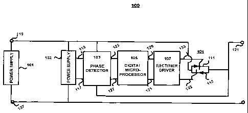
Referring to FIG. 1, an exemplary block diagram-level embodiment is
illustrated for a
controller system 100 to improve efficiency of the operation of a motor (not
shown) by controlling the
power factor of the motor. While a single phase implementation (e.g., single-
phase motor) is
illustrated, those of skill in the art appreciate that multiple stages may be
used to control multi-phase
motors (such as three-phase motors).
The system 100 includes a power supply 101, a power supply 102, a phase
detector 103, a
digital microprocessor 105, a rectifier driver 107, and a rectifier 109. The
power supply 101 is
connected to the phase detector 103 to provide a line voltage 119 via
5a
CA 02654209 2008-12-02
WO 2007/143570 PCT/US2007/070250
a first phase detector input to the phase detector 103 and the power supply
101 is also
connected to a ground 137. The phase detector 103 is also coupled to a motor
terminal
voltage 121 of the motor via a second phase detector input. The phase detector
103 is
coupled to the digital microprocessor 105 to provide signals synchronized to a
zero
crossing of the motor current and a zero crossing of the line voltage 119 to
the digital
microprocessor 105. The digital microprocessor 105 uses the synchronized
signals to
calculate a phase lag of the motor, and hence, the firing time of the
rectifier driver 107.
The rectifier driver 107 fires or turns on the rectifier 109 to command power
to the motor.
A second power supply 102 provides a lower level of the line voltage 119 and
motor terminal voltage 121 into the phase detector 103, where the lower levels
of the line
voltage 119 and the motor terminal voltage 121 of the motor are coupled
respectively to
an input 115 (e.g., +15 Volts) and an input 117 (e.g., -15 Volts) of the phase
detector 103.
The line voltage 119 is also coupled to an input to the rectifier 109. The
first phase
detector output 125 is synchronized to a zero crossing of the motor current
and the
second phase detector output 127 is synchronized to a zero crossing of the
line voltage
119. The first and second phase detector outputs of the phase detector 103 are
coupled to
the digital microprocessor 105. The digital microprocessor 105 senses a first
time at
which a phase of the motor voltage is crossing zero volts and a second time at
which a
phase of the motor current is crossing zero current. Since the digital
microprocessor 105
has an internal clock, the digital microprocessor 105 easily determines the
first and
second times. The digital microprocessor 105 determines the difference in time
between
the first and second times and uses the difference in time to calculate a
phase lag of the
motor. The digital microprocessor 105 uses the phase lag to calculate a firing
time of the
rectifier 109. The firing time varies with at least one of the phase lag and a
load of the
motor.
6
CA 02654209 2008-12-02
WO 2007/143570 PCT/US2007/070250
A first and second output 129 and 131 of the digital microprocessor 105 are
respectively coupled to a first and second input 133 and 135 of the rectifier
driver 107
(e.g., a Silicon Controlled Rectifier (SCR) driver). The first and second
outputs 129 and
131 are synchronized to the zero voltage crossing from the phase detector 103.
The
rectifier driver 107 may be of modern design or similar to those used in the
Nola and
Anderson controllers (discussed above) and may drive any type of thyristors
such as
SCRs and triacs. The rectifier driver 107 controls one or more rectifiers 109
(such as one
or more thyristors 111 and 113 (illustrated in the Nola and Anderson
controllers
discussed above)). The rectifier driver 107 fires the rectifier 109, so that
the motor
terminal voltage 121 will be provided to the motor.
Using the digital microprocessor 105 to determine the motor's phase lag
between
voltage and current and control the rectifier driver 107 permits the
controller system 100
to decrease the phase lag of the motor, which substantially maximizes the
power factor.
Thus, the digital microprocessor 105 can accurately calculate the phase lag of
the motor,
and hence, the firing of the rectifier 109 to efficiently supply power to the
motor.
FIG. 2 illustrates the phase detector 103. Phase detector 103 can be an analog
circuit (e.g., such as the phase detectors used in the Nola and Anderson
controllers). The
phase detector 103 includes one or more voltage dividers to provide voltage
and current
input and one or more operational amplifiers for amplification and conversion
of the
voltage and current waveforms into square waves. The motor terminal voltage
121 is
coupled to a first inverting input 207 of a first operational amplifier 215
(also referred to
as U1) via a first voltage divider 201. The line voltage 119 is coupled to a
first non-
inverting input 209 of the first operational amplifier 215 via a second
voltage divider 203
and a second inverting input 211 of a second operational amplifier 217 (also
referred to
7
WO 2007/143570 CA 02654209 2008-12-02PCT/US2007/070250
as U2) via a third voltage divider. A second non-inverting input of the second
operational amplifier 217 is coupled to ground 137.
The voltage dividers, such as those illustrated with the 50 K ohm and 7.5 K
ohm
resistors, reduce the voltage from a power supply voltage level of the motor
to an
operational amplifier level(s). While these particular resistor values
illustrate an
exemplary embodiment, those of skill in the art clearly recognize that
differing amounts
of voltage adjustment or resistor values may be used depending on the
operating
environment. Differing or additional filter components may be provided to
further
condition the input signals of the first and second operational amplifiers 215
and 217.
The first voltage divider 201 obtains input from the motor terminal voltage
121 and it
feeds to the inverting terminal of the first operational amplifier 215. The
second voltage
divider 203 obtains input from the line voltage 119 and feeds to the non-
inverting
terminal of the first operational amplifier 215. The third voltage divider
circuit obtains
its input from the line voltage 119 and provides a signal to the second
operational
amplifier 217.
A capacitor 221 is coupled between the inverting terminal and the non-
inverting
terminal of the first operational amplifier 215. A capacitor 223 is coupled
between the
non-inverting terminal of the first operational amplifier 215 and the ground
137.
Capacitors 221 and 223 filter noise from the line voltage 119 and the motor
terminal
voltage 121.
The first operational amplifier 215 compares the motor terminal voltage 121 to
the line voltage 119. The first operational amplifier 215 is configured with a
positive
feedback via a resistor 219 (such as the 470 K ohm resistor illustrated). The
positive
feedback causes the first operational amplifier 215 to act as a comparator
with hysteresis.
A first amplifier output (the first phase detector output 125) of the first
operational
8
CA 02654209 2008-12-02
WO 2007/143570 PCT/US2007/070250
amplifier 215 is a square wave synchronized to the phase lag of the motor
current. A
second amplifier output (the second phase detector output 127) of the second
operational
amplifier 217 operates as square wave generator that produces square waves
synchronized to the zero crossings of the line voltage 119. The first
amplifier output 125
of the first operational amplifier 215 is synchronized to a zero crossing of
the motor
current and the second amplifier output 127 of the second operational
amplifier 217 is
synchronized to a zero crossing of the line voltage 119.
Alternatively, the first voltage divider 201 can be replaced by a current
transducer
(not shown). The current transducer also replaces the resistor 219 and the
second voltage
divider 203 coupled to the first operational amplifier 215. As such, the
current transducer
can measure the zero crossing of the current of the motor.
The digital microprocessor 105 is coupled between the phase detector output of
the first and second amplifier outputs 125 and 127 and the rectifier driver
107. The
digital microprocessor 105 determines a phase lag (e.g., a phase angle
difference) of the
IS current and voltage of the motor by calculating the time difference
between a switching
state of the first operational amplifier 215 and a switching state of the
second operational
amplifier 217, which produces an instantaneous signal of phase lag. The phase
lag is
used in order to control the firing of the rectifier driver 107. Thus, the
firing of the
rectifier driver 107 fires the rectifier 109 to supply power to the motor.
FIG. 3 illustrates nominal waveforms for the line voltage 119 and the motor
current produced by the output of the system 100 together with the
corresponding outputs
of the first and second operational amplifiers 215 and 217.
To understand how phase is detected, it is helpful to consider the output of
the
first operational amplifier 215. When the thyristors 111 and 113 are switched
off (zero
motor voltage), the difference between the inverting and non-inverting
terminals of the
9
WO 2007/143570 CA 02654209 2008-12-02PCT/US2007/070250
first operational amplifier 215 is equal to the line voltage 119 sensed.
However, when
the thyristors 111 and 113 are turned on, the voltage difference between the
line and
motor terminals will be very low. When the sensed line voltage 119 (non-
inverting
input) is greater than the sensed motor voltage (inverting input), the output
of the first
operational amplifier 215 is +15 volts. This occurs, for example, during the
positive half-
cycle of line voltage 119 when the thyristors 111 and 113 are off indicated by
zero
current. The positive output of the first operational amplifier 215 combined
with the
positive feedback increases the line voltage 119 sensed, such that the first
operational
amplifier 215 will not change state until the sensed motor voltage (inverting
input) is
significantly greater than the sensed line voltage 119. This does not occur
until the
thyristors 111 and 113 are again off during the negative half cycle of line
voltage 119.
Therefore, the output of the first operational amplifier 215 will be positive
from the time
the thyristors 111 and 113 turn off on the positive half-cycle of line voltage
119 until the
thyristors 111 and 113 again turn off on the negative half-cycle of line
voltage 119. This
waveform is illustrated in FIG. 3 as the first operational amplifier 215.
The second operational amplifier 217, on the other hand, senses only the line
voltage 119 and changes state from positive to negative as the line voltage
119 changes
from positive to negative.
Consequently, the digital microprocessor 105 (or a microcontroller or digital
signal processor) can be used to determine the phase angle by calculating the
time
difference between the switching state of the first operational amplifier 215
and the
switching state of the second operational amplifier 217. This produces an
instantaneous
signal of phase angle. The phase detection algorithm is:
y = (Ti T2) x K Equation No. 1
10
CA 02654209 2008-12-02
WO 2007/143570 PCT/US2007/070250
Where Ti = time current crosses zero
T2 = time voltage crosses zero
K = 360 degrees divided by the time of one voltage cycle in
milliseconds for the difference between Ti and T2 expressed in milliseconds
= phase lag in degrees
The phase lag is used to calculate the firing (on and off times) of the
thyristors
111 and 113.
The digital microprocessor 105 (or a microcontroller or digital signal
processor)
can be used to determine a phase error signal associated with the phase lag by
calculating
the time difference between the switching state of the first operational
amplifier 215 and
the switching state of the second operational amplifier 217. The phase error
detection
algorithm is:
(OD - OFB) x K = X Equation No. 2
Where OD = desired phase angle in milliseconds
OFB = zero crossing time of motor current minus zero crossing
time of motor voltage in milliseconds
K = 360 degrees divided by the time of one voltage cycle in
milliseconds (e.g., for 60 cycle voltage, 360 degrees is divided by a time
16.667
milliseconds)
X = phase error signal in degrees
11
CA 02654209 2008-12-02
WO 2007/143570 PCT/US2007/070250
While K in Equation No. 1 is expressed in time (more generally), K in Equation
No. 2 is expressed in milliseconds. The phase error signal is used in system
100 to
control the firing (on and off times) of the thyristors 111 and 113.
For example, FIG. 4 depicts curves 4a through 4e as a typical set of motor
characteristics
relating phase angle to when thyristors 111 and 113 are turned back on, a time
referred to as the
firing angle. Illustrated in FIG. 4 is a straight line extending upward and to
the right, where an
equation describing this line is:
y = Ax -B Equation No. 3
Where X = the measured phase angle (which can be 7 in Equation No. 1)
A = the gain (e.g., the gain is 4 in FIG. 4)
B = an offset ((e.g., the offset is 128 in FIG. 4)
y = the firing angle
Curve 4a, with a vertical portion having a phase lag of about 50 degrees is
shown for a
fully loaded motor (100%); whereas, the curve 4e with the vertical portion
having a phase lag of
about 75 degrees is illustrated for an unloaded motor (0%). The curves in
between (at 4b, 4c,
and 4d) are illustrative of motor loads in between the fully loaded and
unloaded motor
operational ranges (75%, 50%, and 25% loaded, respectively).
In an exemplary embodiment in curves 4a through 4e, the thyristor 111 (or
thyristor 113)
is commanded to turn off at a zero voltage crossing. However, because there is
current passing
through thyristor 111, thyristor 111 cannot turn off until this current goes
to zero. At some time
after the zero voltage crossing, this current goes to zero (e.g., the phase
lag time). At this time,
the thyristor 111 turns off (unless thyristor 111 was commanded to fire on by
the controller
system 100 before this zero current crossing). If thyristor 111 was commanded
to fire on by the
12
CA 02654209 2008-12-02
WO 2007/143570 PCT/US2007/070250
controller system 100 before this zero current crossing, then thyristor 111
stays on. When the
firing time is less than the phase lag time, the thyristor 111 stays on and
the phase lag stays
constant.
For firing times greater than the phase lag, the thyristor 111 will turn off
at the zero
current crossing (phase lag) and back on at the firing time. This will cause
the motor to receive
zero volts while the thyristor 111 is off. The average voltage over the full
cycle will be lower
and the phase lag will be less (i.e., higher power factor). By increasing the
firing time above the
point where phase and firing time are equal at a given load, the curves 4a
through 4e of FIG. 4
are generated. Curves 4a through 4e represent the motor's characteristics or
the relationship of
phase to firing time for the motor.
For example, it is desirable to have close to full voltage for full load, as
in curve 4a, and
minimum phase lag for no load, as in curve 4e. In this example, the system 100
outputs a firing
angle of about 50 degrees at full load, in curve 4a, and about 110 degrees at
no load, in curve 4e.
Unfortunately, firing at 110 degrees for no load, the motor shuts down because
the motor does
not have enough voltage to run. At a firing angle of 100 degrees and no load,
the phase will be
about 57 degrees, and at a firing angle of 55 degrees the phase will be about
46 degrees. Using
these two points, the desired firing angle can be calculated (e.g., using
Equation No. 3). For a
load of curve 4d, the system 100 will fire where the line represented by
Equation No. 3 crosses
the curve 4d. The system 100 controls the motor at the intersection of the
line represented by
Equation No. 3 and the current load curve. When the load changes, the phase
angle moves to the
new intersection of the new load curve and the line represented by Equation
No. 3. This is
closed loop feedback control in that as the input (which is phase) changes,
the output changes
automatically. Equation No. 3 can be adjusted by those skilled in the art
using closed loop
feedback control principles to stabilize the system 100. For example, if
Equation No. 3
13
CA 02654209 2008-12-02
WO 2007/143570 PCT/US2007/070250
approached a vertical straight line (where y = 20x -1000), the feedback
control system of the
motor would be unstable.
Equation No. 3 describes one exemplary embodiment of an algorithm for
controlling the
phase angle of the motor of the system 100. The algorithm for controlling the
phase angle may
be adjusted by varying the constant 128 and the gain 4. One exemplary
implementation of the
algorithm for controlling the phase angle is illustrated in FIG. 5.
FIG. 5 illustrates a block diagram for one embodiment of the phase angle
control
algorithm implemented in the digital microprocessor 105 illustrated in FIG. 1.
The phase angle
control algorithm may be adjusted by varying the constant 128 and the gain 4,
such as in
Equation No. 3. Put another way, the exemplary embodiment in FIG. 5 calculates
the firing time
in milliseconds in part by solving Equation No. 3, but various other equations
can be used.
System 100 controls the firing of the thyristors 111 and 113 by using the
digital microprocessor
105 to calculate a time derived phase angle (e.g., the output of step 505 in
Figure 5 and Equation
No. 1) and uses this phase angle in the digital microprocessor 105 to
calculate a thyristor firing
time using Equation No. 3.
For example, a zero crossing time of the voltage of the motor is calculated by
the digital
microprocessor 105 (such as in milliseconds) (step 501). A zero crossing time
of the current of
the motor is calculated by the digital microprocessor 105 (such as in
milliseconds) (step 503).
The digital microprocessor 105 calculates the difference in time between the
zero crossing times
of the motor current and motor voltage (step 505). This difference in time is
used to calculate a
phase lag between the voltage and current of the motor (e.g., difference in
time multiplied by
21.6 degrees/milliseconds) (step 507). The digital microprocessor 105
multiplies this phase lag
by a gain (e.g., 4 from Equation No. 3) (step 509). The digital microprocessor
105 uses this
phase lag from step 509 with an offset (e.g., subtract 128 degrees from the
phase lag from step
509) (step 511) to calculate a firing angle of the rectifier driver 107 (e.g.,
a firing angle in
14
WO 2007/143570 CA 02654209 2008-12-02 PCT/US2007/070250
degrees) (step 513). The offset of 128 degrees comes from Equation No. 3. The
digital
microprocessor 105 uses the firing angle from step 513 and multiplies it by
0.046 (step 515) to
convert the firing angle from degrees to milliseconds. The firing angle in
milliseconds is used
with the zero crossing time of the voltage of the motor to calculate the
firing time of the rectifier
driver 107 (e.g., such as in milliseconds) (step 517).
One voltage sine wave is 360 degrees and 0 degrees is at the zero crossing. A
firing
angle of 90 degrees occurs at the peak of such a sine wave. The firing time is
in milliseconds.
For a 60 cycle AC voltage, one sine wave is 16-2/3 milliseconds from start to
finish. For a firing
angle of 90 degrees, the firing time is 1/4 of 16-2/3 milliseconds (or 4.166
milliseconds). The
it) 21.6 degrees/milliseconds comes from 360 degrees divided by 16-2/3
milliseconds. The 0.046
comes from 16-2/3 milliseconds divided by 360 degrees.
It can be appreciated that those skilled in the art may modify the numbers
associated with
the algorithm as well as the elements of the system 100 such as adding a
Proportional Integral
Differential (PID) controller or other similar control devices to optimize the
system 100 and
compensate for instability if desired. Thus, use of the aforementioned
approach along with the
improved detection of phase lag (power factor) using the digital
microprocessor 105 is one
exemplary embodiment of the present invention.
FIG. 6 illustrates a method for power factor control of a motor including
sensing the zero
crossings of the voltage and current of the motor to determine a time
difference to calculate a
phase lag of the motor. This method includes running the power of the motor
fully for a number
of cycles (X) to get the motor up to full operating speed (step 601). A
determination is made to
detect a zero crossing of the voltage of the motor (step 603). Using the
digital microprocessor
105, a first time at which a phase of the motor voltage is crossing zero volts
is sensed. A timer
or timing loop in the digital microprocessor 105 is started upon detecting the
zero voltage
crossing of the voltage of the motor (step 605). A determination is made to
detect a zero
15
CA 02654209 2008-12-02
WO 2007/143570 PCT/US2007/070250
crossing of the current of the motor (step 607). Using the digital
microprocessor 105, a second
time at which a phase of the motor current is crossing zero current is sensed.
The first and
second times are used to calculate the phase lag of the motor (step 609).
Using the digital
microprocessor 105, the difference in time between the first and second times
is determined.
Using the digital microprocessor 105, the difference in time is used to
calculate a phase lag of the
motor. The firing angle is calculated based on the phase lag of the motor
(step 611). The firing
angle determines when to fire the rectifier driver 107, and consequently the
rectifier 111 (step
613). Steps 603 through 613 are repeated to provide power factor control of
the motor by
sensing the zero crossings of the voltage and current of the motor to
determine the time
difference to calculate the phase lag of the motor. Thus, using the digital
microprocessor 105,
the phase lag is used to calculate a firing time of a rectifier 109, where the
firing time varies with
at least one of the phase lag and a load of the motor.
The present invention has been described with reference to specific exemplary
embodiments. However, it will be appreciated that various modifications and
changes can be
made without departing from the scope of the present invention. The
specification and figures
are to be regarded in an illustrative manner, rather than a restrictive one,
and all such
modifications are intended to be included within the scope of present
invention.
Benefits, other advantages, and solutions to problems have been described
above with
regard to specific exemplary embodiments. However, the benefits, advantages,
solutions to
problems, and any element(s) that may cause any benefit, advantage, or
solution to occur or
become more pronounced are not to be construed as critical, required, or
essential features or
elements. As used herein, the terms "comprises", "comprising", "including", or
any variations
thereof, are intended to cover a non-exclusive inclusion, such that a process,
method, article, or
apparatus that comprises a list of elements does not include only those
elements but may include
other elements not expressly listed or inherent to such process, method,
article, or apparatus.
16
WO 2007/143570 CA 02654209 2008-12-02PCT/US2007/070250
Further, no element described herein is required for the practice of the
invention, unless
expressly described as "essential" or "critical".
17