Note: Descriptions are shown in the official language in which they were submitted.
CA 02654453 2008-12-05
WO 2007/140537 PCT/AU2007/000802
PRODUCTION OF MICROFLUIDIC DEVICES
USING LASER-INDUCED SHOCKWAVES
CROSS REFERENCE TO RELATED APPLICATIONS
This application claims priority from US provisional patent application number
60/811,437, filed on 7 June 2006 the entire contents of which are incorporated
herein
by reference. This application also claims priority from Australian
provisional patent
application AU 2006903098 filed on 7 June 2006, the entire contents of which
are
incorporated herein by reference.
This application also claims priority from International (PCT) application
PCT/IB2006/003311, filed on 22 November 2006, the entire contents of which are
incorporated herein by reference. This application also claims priority from
International (PCT) application PCT/AU2007/000012, filed on 11 January 2007,
the
entire contents of which are incorporated herein by reference. This
application also
claims priority from International (PCT) application PCT/AU2007/000061, filed
on 24
January 2007, the entire contents of which are incorporated herein by
reference.
This application also claims priority from International (PCT) application
PCT/AU2007/000062, filed on 24 January 2007, the entire contents of which are
incorporated herein by reference. This application also claims priority from
International (PCT) application PCT/AU2007/000435, filed on 10 April 2007, the
entire contents of which are incorporated herein by reference.
FIELD OF THE INVENTION
This invention relates generally to manufacturing methods and devices for
laser machining single or multilayer materials. The field of this invention
also extends
to the manufacture of components relating to food and pharmaceutical, medical,
invitro diagnostic, and microfluidic devices and packaging.
BACKGROUND OF THE INVENTION
The present invention reiates generally to manufacturing methods and devices
for laser machining materials. Typically laser processing of devices has been
in the
areas of laser cutting, surface machining, surface treatment, and laser
welding. Laser
cutting typically involves cutting entirely through a substrate; surface
machining
techniques selectively remove parts of a substrate; physical surface treatment
1
CA 02654453 2008-12-05
WO 2007/140537 PCT/AU2007/000802
involves melting or etching the surface, whereas chemical surface treatment
typically
operates below the ablation threshold to modify the surface properties; and
laser
welding typically involves selectively melting the interfacial material
between two
surfaces, and can be performed by either direct surface exposure, or through
the use
of transmission or reverse conduction welding for joining internal surfaces.
Scanned
beam systems are known for all methods and lithographic systems have been used
for structuring and surface modification depending on the energy density,
material
properties, resolution, and throughput required.
Applications for the laser processing of multilayer materials typically
involve
the removal of outer layers of material, such as the stripping of insulation
off wires or
exposing electrodes on printed circuit boards, or welding via transmission and-
reverse conduction methods.
Transmission laser welding operates by one material being transparent to and
the other material being an absorber of the irradiated laser wavelength. This
allows
the laser beam to selectively heat between the two materials producing
localised
welding when the heat rises above the glass transition temperature. For
integration
into the production environment, the main limitations are processing times,
and
limitation of compatible materials and number of layers that can be processed.
Reverse conduction welding operates in a similar manner to transmission
layer welding except that the heat is generated by laser absorption at a
backplane.
The polymer films clamped above the absorbing layer conduct the heat from its
surface and locally melt. Due to uniform heat conduction within the polymers
which.
limits spatial resolution, the technique is only suitable for thin films and
relatively
large structures.
More recently specific laser absorbers, such as Clearweld , have been used
for bonding. In practice this material is difficult to apply to mass
production of micro-
machined substrates and produces a slightly opaque weld that can reduce the
appeal of a product or interfere with the operation, for example, sensor
response, of
some devices.
Lasers have also been used for micromachining substrate surfaces. These
techniques usually employ ultraviolet (UV) lasers, typically excimer lasers,
which can
produce fine anisotropically etched structures down to one micron.
Unfortunately
such systems are expensive and relatively slow to process material. More
recently,
focus has been on the use of shorter wavelength UV lasers that can machine
2
CA 02654453 2008-12-05
WO 2007/140537 PCT/AU2007/000802
channels down to 100 m, depending on the material thickness. Unfortunately
such
systems provide a large heat-affected zone that limits fine structures, such
as those
required for microfluidic geometries. In a similar manner, infrared (IR) YAG
and CO2
lasers have been demonstrated for microfluidic channel fabrication for large
structures only (in the order of hundreds of microns).
The challenge in incorporating such technologies into manufacturing
processes relates to the time required for the laser to complete its machining
process
as well as the quality morphology of the resulting cut or machined surface.
The reference to any prior art in this specification is not, and should not be
taken as, an acknowledgement or any form of suggestion that the prior art
forms part
of the common general knowledge.
SUMMARY OF THE INVENTION
The invention provides methods for laser structuring of single and multi-
layered materials. The invention includes apparatus, methods and products.
The method, apparatus and devices of the present invention have many
advantages, including in various embodiments, for example:
- a smaller heat affected zone
- improved structure feature size
- improved structuring accuracy
- improved structuring precision
- simplified fabrication of parts with unsupported structures
- use of cheaper lasers such as IR YAG and C02 lasers for
microstructuring
- parallel processing
In a first aspect of the invention, there is provided a method for
manufacturing
at least part of a device comprising a substrate wherein at least one laser is
used to
alter a portion of the substrate during the manufacturing process. Certain
embodiments provide such a method for manufacturing at least part of a
multilayered
device comprising use of at least one laser to alter at least one layer of
said part
during the manufacturing process.
In a second aspect of the invention, there is provided, an apparatus for
manufacturing at least part of a device comprising a substrate, the apparatus
comprising at least one laser source to produce a laser beam to alter at least
one
3
CA 02654453 2008-12-05
WO 2007/140537 PCT/AU2007/000802
portion of the substrate during the manufacturing process. Certain embodiments
provide such an apparatus for manufacturing at least part of a multilayered
device
comprising at least one laser source to produce a laser beam to alter at least
one
layer of said part during the manufacturing process.
In a third aspect of the invention, there is provided a part of a device
manufactured according to the process or using the apparatus of the present
invention.
In a fourth aspect of the invention, there is provided a device manufactured
according to the process or using the apparatus of the present invention.
Some preferred embodiments are particularly adapted to manufacture of
specialist devices, such as microfluidic devices.
Any suitable laser with any suitable characteristics may be used in the method
or apparatus of the present invention. For example, in some embodiments, a
variety
of wavelengths are utilized and in others, a plurality of laser beams.
In embodiments which comprise a plurality of laser beams, the laser beams
may for example improve the formed structure and / or simplify the
manufacturing
process. In some embodiments, the plurality of laser beams use at least one
part of
the same alignment system. The plurality of laser beams may interact with each
other or be used in ways which enhance the overall processing. Thus, for
example,
the plurality of laser beams may operate at least partially simultaneously or
they may
operate optionally at least partially concurrently or at least partially
intermittently. The
plurality of laser beams may also be operated with one or more timing
characteristics.
In some embodiments, the laser beam energy is increased which may for
example enable faster processing. Thus in some embodiments, the increased
laser
beam energy enables alteration of the dominant processing mechanism, which is
optionally one or more of thermal melt, plasma formation, ablation by bond
cleavage
and subsequent volume expansion, and multi-photon bond dissociation.
Embodiments with a plurality of laser beams may also enable simplified
manufacturing processing, for example by reducing cost, improving alignment,
increased speed of processing, and optionally for example when a plurality of
beams
use parts of the same alignment system.
In some embodiments, a first laser beam and a second laser beam work in
conjunction with one another. In one such embodiment, a first laser beam forms
a
melt and a second laser beam removes material, optionally by laser induced
4
CA 02654453 2008-12-05
WO 2007/140537 PCT/AU2007/000802
shockwaves and optionally by a pulsed laser beam. In another embodiment, a
first
laser beam increases bond or lattice energy to an excited state and a second
laser
beam removes material, optionally with an increased energy density. In a
further
embodiment, a first laser beam removes material and a second laser beam alters
surface morphology, optionally by inducing surface reflow for reshaping,
debris
minimisation, crystallinity changes, and/or surface chemistry alteration. In
some
embodiments a first laser beam having a first wavelength is used to target a
first
portion of substrate and a second laser beam having a second wavelength is
used to
target a second portion of substrate. In some of these embodiments applicable
to
multilayered devices, the first laser targets a first layer and the second
laser targets a
second layer. In other embodiments, the first laser beam targets a particular
chemical bond in the substrate and a second laser beam having a second
wavelength is used to target a different chemical bond in the substrate.
In some embodiments which comprise a plurality of laser beams, the beams
may be combined prior to falling incident on a portion of substrate or a
layer.
Combination of the beams may be by any suitable method, for example, by using
an
optical element, such as a mirror or lens. In some embodiments, the plurality
of laser
beams originally arise from the same source.
The material to be lasered may be of any suitable form. Some preferred
embodiments comprise the use of an additive in a layer to alter the effect of
a laser
beam on that or another layer. Thus, for exampie, the additive may affect and
optionally improve radiatiori absorption at the laser's wavelength. Equally,
however,
it may increase transmission of a laser beam through the substrate and
consequently
indirectly affect the substrate or layer below. Some embodiments comprise the
use
of a portion of substrate (which may for example, be a layer) with an
absorption and /
or reflection characteristic to influence the effect of the laser. The
characteristic may
be of any suitable form, for example, it may allow selective machining of an
absorbing portion of substrate (which may for example, be a layer).
Other suitable aspects of the material to be lasered may be provided, altered,
or optimised. For example, the material may comprise a thermally conductive
portion
(which may for example, be a layer) for improved structure formation.
Various thermal techniques may also be used as part of the present invention,
For example, heat may be reduced or guided to provide improved structure
geometry
or reduce the effect of the machining process on the surrounding materials and
5
CA 02654453 2008-12-05
WO 2007/140537 PCT/AU2007/000802
structures.
Various masking techniques may also be used as part of the present
invention. Thus, one embodiment comprises the use of a masking component
between the laser source and a portion of substrate (such as a layer) to limit
or alter
exposure to the laser beam on an area of the substrate or layer. The mask or
masking component may take any suitable form, for example, in applications
relating
to multi-layer devices, the masking component may itself be a portion of the
substrate or a layer.
The present invention may also be used to increase throughput, for example
by providing parallel processing. In some such embodiments a masking component
may contribute to alignment of parts during manufacture. In some embodiments a
masking component provides greater spatial resolution. The masking component
may perform one or more functions, such as for example: conducting heat away
from
an area on a portion of substrate, such as a layer, (b) protecting a surface
from
debris, and / or (c) supporting one or more structures during processing.
The present invention may be further optimised with the use of an optical
component to alter or focus the laser beam. The optical component may take any
suitable form, for example it may comprise one or more lenses, prisms or other
refractive, diffractive or reflective elements. In some embodiments, the
optical
component simplifies alignment of parts during processing. The optical
component
may perform one or more functions such as for example, altering one or more of
the
frequency, intensity, direction, duration or timing of the laser beam.
In some embodiments of the present invention, a portion of substrate such as
a layer may be removed during or after the manufacturing process. The use of
such
a removable portion of substrate or layer, in some situations referred to as a
sacrificial portion or sacrificial layer, can add further benefits to the
present invention.
In some embodiments which comprise such a portion of substrate or layer which
is
removed, the removed portion may perform one or more of the following
functions:
protect a surface from debris, thermal conduction, support cut out or free
standing
structures, focus or mask a beam, allow a secondary machining process to
occur.
The substrate material and / or layers the subject of the laser processing and
/
or manufacturing of the present invention may be of any suitable type. Thus,
for
example, they may comprise one or more of polymer, metal, metal oxide, metal
foil,
paper, nitrocellulose, glass, silicone, photo-resist, ceramic, wood or fabric.
6
CA 02654453 2008-12-05
WO 2007/140537 PCT/AU2007/000802
The process flow of a method and apparatus according to the present
invention may be arranged in any suitable manner. In some embodiments, the
process utilizes an at least semi-continuous web while in others, the process
is not
web-based.
The method and apparatus of the present invention is also particularly suited
to the use of additional non-laser processing steps which may occur before,
during or
after a laser step. Any suitable non-laser step may be used in conjunction
with the
present invention. Thus, in some embodiments, a non-laser process step
comprises
one or more of injection molding, micromilling, die cutting, hot foil
stamping,
stamping, embossing, thermoforming, print-head deposition, photolithography,
coating, curing. In some embodiments, a non-laser processing step comprises a
pre-treatment process, which may for example reduce the heat affected zone
from
the laser machining process. A pre-treatment process according to the present
invention may comprise any suitable steps, thus for example, it may comprise
one or
more of: providing cooling or heat sinking to parts of the material, or
modifying the
material's surface or bulk properties to alter the thermal conductivity or
absorption
characteristics.
In some embodiments, there is further provided a post-treatment process
which may for example optionally structure, cure, surface treat, coat or
render one or
more parts.
The application of thermal energy, or heat is one example of a non-laser
processing step which may have particular benefits. In one embodiment, one or
more of the area of the substrate or layer to be laser treated, the local area
on the
substrate or a tool may be heated to improve material flow around a tool. Any
suitable tool may be used, for example, it may be an embossing tool. In one
embodiment, a laser beam is scanned over an area to be embossed. Such scanning
may occur at any suitable timed, for example prior to, during or after
embossing.
In some embodiments, a structure is formed by selectively applying a laser to
a defined area of a substrate or layer to thereby weaken it. Such a process
step may
be used to make a wide variety of useful structures, for example, burst
valves,
tearing guides, perforations, meshes, etc. Some embodiments utilise the laser
to
alter the barrier properties of a portion of substrate or layer by selective
application of
the laser. This may occur by any suitable means, for example a series or
network of
perforations through a portion of substrate or layer.
7
CA 02654453 2008-12-05
WO 2007/140537 PCT/AU2007/000802
A laser treatment step according to the present invention may occur at any
suitable stage. For example, a component part of a device to be manufactured
in
accordance with the invention may be laser treated prior to or after assembly
of the
device. In some embodiments, assembly of a multilayered device comprises laser
treatment. This may occur for example where assembly comprises a laser-
treatment
bonding step which may for example comprise laser assisted bonding of layers.
Precision alignment is a very important part of certain embodiments of the
present invention. In some embodiments, the method or apparatus comprises the
use of one or more alignment marks, notches, grooves, or edge guides for
alignment.
Some embodiments also comprise the use of a control system. Any suitable
control
system may be used, for example it may comprise one or more of: mechanical
sensor feedback, optical sensor feedback, part translation and / or laser
scanning
adjustment.
Throughout this specification (including any claims which follow), unless the
context requires otherwise, the word `comprise', and variations such as
`comprises'
and `comprising', will be understood to imply the inclusion of a stated
integer or step
or group of integers or steps but not the exclusion of any other integer or
step or
group of integers or steps.
BRIEF DESCRIPTION OF DRAWINGS
Figures 1A and 1B are schematic representations of examples of
combinations of multiple laser beams.
Figure 2 is a schematic representation of a card or sheet production system.
Figure 3 is a schematic representation of a web or continuous production
system.
Figure 4 is a schematic representation of a combined laser and embossing
process.
Figure 5 is a schematic representation of a simultaneous laser and embossing
process.
Figure 6 is a schematic representation of laser structuring in multilayer
devices
with and without heat conductive layers.
Figure 7 is a schematic representation of selective laser machining of layers
in
a multilayer device.
Figure 8 is a schematic representation of the use of reflective lasers during
8
CA 02654453 2008-12-05
WO 2007/140537 PCT/AU2007/000802
laser machining in a multilayer device.
Figure 9 is a schematic representation of examples of microfluidic fabrication
by laser machining.
Figure 10 is a schematic representation of an example of a microfluidic device
=
fabricated through a transparent layer by laser machining.
Figure 11 is a schematic representation of the use of masking on a multilayer
device for laser processing.
Figure 12 is a schematic representation of the use of optical components on a
multilayer device for laser processing.
Figure 13 is a schematic representation of the use of protective layers during
the laser machining process.
Figure 14 is a schematic representation of examples of burst valve formation
by laser machining.
Figure 15 is a schematic representation of an example of a tear structure
machined into a multilayer device.
Figure 16 is a schematic representation of an example of modification of a
multilayer device for controlled barrier layer properties.
DETAILED DESCRIPTION OF THE INVENTION
It is convenient to describe the invention herein in relation to particularly
preferred embodiments relating to food and pharmaceutical, medical, invitro
diagnostic, and microfluidic devices and packaging. However, the invention is
applicable to a wide range of situations and products and it is to be
appreciated that
other constructions and arrangements are also considered as falling within the
scope
of the invention. Various modifications, alterations, variations and or
additions to the
construction and arrangements described herein are also considered as falling
within
the ambit and scope of the present invention.
As used herein, the term "fluid" refers to either gas or liquid phase
materials.
As used herein, the term "microfluidic" refers to fluid handling,
manipulation, or
processing carried out in structures with at least one dimension less than one
millimetre. As used herein, the term "beam" or "ray" refers to more than one
photon
travelling in a substantially similar direction. Laser machining techniques
used in the
present invention include, but are not limited to, scanned beam and
lithographic
9
CA 02654453 2008-12-05
WO 2007/140537 PCT/AU2007/000802
systems. Laser and material interactions used in the present invention may be
of any
suitable type, and may for example include photo-thermal, photo-chemical
processes
or combinations of the two.
The laser beam incident on the substrate or material may be from a single
laser or a plurality of lasers. Where multiple laser beams are combined to
machine
the work-piece, the beams may operate simultaneously or with different timing
characteristics. For example laser beams may operate at the same or different
wavelengths irradiating the same area either, alternatively, concurrently, or
simultaneously at different switching frequencies.
Various improvements are made possible by combining multiple beams, such
as for example, increasing beam energy density to provide faster processing.
In
addition, a combination of multiple beams increases beam energy density which
enables alteration of the dominant processing mechanisms, such as thermal
melt,
plasma formation, ablation by bond cleavage and subsequent volume expansion,
and multi-photon bond dissociation. Furthermore, a combination of multiple
beams
may simplify manufacturing implementation by reducing alignment issues and by
increasing the speed of processing when the beams are delivered using the same
alignment mechanism. Some examples include: alignment mechanisms may be in
the form of the laser beams using separate optical paths and a common
alignment
controller, or the beams may share a common optical path, such as where the
laser
beam guiding stage is common to both beams. An example of this would be where
galvo mirror scanners or x-y driven output optics are common to both laser
beams.
Such improvements in manufacturing are particularly important for micro-
structuring
to avoid the use of additional costly alignment systems, which would also
introduce a
further tolerance requirement associated with the error in beam placement
between
the multiple alignment systems. A further advantage of using multiple beams is
that
it enables the use of multiple processing methodologies which mean faster
processing and improved structure formation. This may be done in various ways,
for
example:
o Melt formation from a first laser beam and material removal by laser
induced shockwaves from a second laser beam. Examples include the
combination of a continuous laser beam for melt formation with a pulsed
laser beam to induce material removal.
o Using a first laser beam to increase bond energy and a second laser beam
CA 02654453 2008-12-05
WO 2007/140537 PCT/AU2007/000802
to remove material. The first laser beam increases bond or lattice energy
to an excited state, but does not increase energy density to the point that
the bonds dissociate. The second laser beam, which has greater photon
energy is used to induce bond dissociation and therefore removal of
material.
o Material removal by a first laser beam and surface morphology alteration
by a second beam. The second beam may for example induce surface
reflow for reshaping, debris minimisation, crystallinity changes, and/or
surface chemistry alteration. Either laser beam may use thermally or.
ablative mechanisms.
o A first laser beam induces a material change, such as crystallinity, bond
chemistry, or surface morphology, and a second laser beam removes
material. For example the first laser beam may increase the absorption
characteristics of the material to the second laser beam, or alternatively be
used to selectively reduce the absorption characteristics of the material to
the second laser beam.
o Use of laser beams with different wavelengths to target different
processing materials. Thus, for example, different bond or vibrational
energies may be targeted in the same material by different wavelengths, or
the different lasers may target different materials or layers when multiple
materials are processed, as with multilayered devices.
In one embodiment, multiple laser beams are combined prior to irradiating the
material; as shown in Figure 1A in which beams (3, 4) from two separate lasers
(1,2)
are combined by reflective mirrors (5,6,7,8) and lens system (9) to machine
the work-
piece (10). Figure 1 B illustrates an example in which a laser beam (12) from
a single
laser source (11) is split at the partially reflective mirror (13) into two
separate beams
(22,23) with one beam (22) being altered (in timing or wavelength) by the
altering
system (19), which could for example be a delay line, switched gate, or
frequency
multiplier, before being recombined through the mirror elements (15,16,17,18)
and
lens system (20) to machine the work-piece (21). Altering of the Laser beams
may be
by any suitable means, for example, (a) frequency, such as a frequency
multiplicatiori
as for example by a YAG Laser beam that has its fundamental frequency of
1.06pm
quadrupled to 266nm, or (b) duration, such as a continuous wave laser beam
that is
11
CA 02654453 2008-12-05
WO 2007/140537 PCT/AU2007/000802
switched to a pulsed waveform.
The laser machined structures may be fabricated on discrete parts or onto
reels of continuous material. Figure 2 shows one embodiment of a production
line
used to structure discrete parts or items such as cards. In this example the
laminated
material may be stamped in the system prior to lamination or be converted as a
separate process. The process depicts input/output hoppers (24,25) and a card
handling system that accepts cards (26) in ISO 7816 format material. The
processes
which are sequentially operating on the cards include: laser machining system
(27),
overlay laminating (28) of preformed laminates (32), embossing (29), topping
(30),
and finally programming or encoding (31).
An example of a production line for the fabrication of continuos parts, or
onto a
web, is illustrated in Figure 3. . In this example, the modular production
units depicted
are interspersed with material feed handlers (43) and include: forming stock
material
inputs (33), blister forming (34), filling (35), bonding (36), printing (37),
curing (38),
tension control (39), material guides and unwinds (40), laser structuring
through
composite materials (41), die cutting (42), and final part collection (44).
Structures produced according to the present invention may be cut, rendered
or divided into smaller parts.
In one embodiment of the invention, laser machined parts are bonded to other
components, which may or may not be a continuous substrate, and may or may not
be planar, and may be made of single or multiple components.
In another embodiment, the laser machining processes may be combined with
other structuring processes; such as injection molding, micromilling, die
cutting, hot
foil stamping, stamping, embossing, thermoforming, print-head deposition,
photolithography, coating, curing and other structuring methods.
The present invention may also be combined with other processes to facilitate
the laser machining process or improve the performance of laser machined
devices.
For example the present invention may be combined with one or more pre-
treatment
processes to reduce the heat affected zone from the laser machining process.
Such
pre-treatment may include providing cooling or heat sinking to parts of the
material,
or modifying the material's surface or bulk properties to alter the thermal
conductivity
or absorption characteristics. Post-treatment processes may also be used to
structure, cure, surface treat, coat or render the parts. For example
PCT/AU2007/000061 describes a combined laser embossing process that enables
12
CA 02654453 2008-12-05
WO 2007/140537 PCT/AU2007/000802
more rapid replication of embossed features than normal and hot embossing. By
pre-
treating the local area to be embossed with lasers, the local material is
altered, which
allows (a) lowering of the softening point (as is especially the case with
orientated
films), preheating of the exposed area, (b) material reflow and (c) in some
cases,
ablation from the embossed area.
After laser processing, and before stamping, the area of the film to be
treated,
the local area on the substrate or the tool may be heated to improve the
material flow
around the tool. The laser beam may expose the entire substrate surface or
just the
area to be embossed, as illustrated in Figure 4 in which a focused laser beam
(45) is
scanned over the embossed area (46) prior to embossing (49). The material in
the
embossing area (46) then forms around the embossing tool (47) during embossing
(50), replicating the tooling structure into the material (48) when the tool
(47) is
removed (51). Such a process allows the use of longer wavelength lasers than
the
expensive and slower UV excimer systems for fine structure formation. Unlike
their
excimer counterparts, such longer wavelength systems produce more thermal
damage and typically have larger focus spot sizes, which severely limits their
spatial
resolution for micro-structuring. By combining the laser machining process
with
embossing, finer and more accurately formed microstructures may be fabricated
than
with the laser alone, and larger structures may be formed than with embossing
alone.
Thereby providing a much faster and cheaper method than excimer laser
processing.
Similarly, the swarf and rough edges produced by the laser cutting processes
may
also be processed after structuring to improve channel performance.
The combination of other processes with laser process may occur either
simultaneously or in any order. In some embodiments, it occurs simultaneously.
For
example, in one embodiment an embossed material is laser machined during the
embossing processes. Whilst the embossing tool is pressed to the surface of
the
material, the laser irradiates the reverse side of the material to cause
localised reflow
around the tool to improve the speed of embossing, and or the replication of
the
structure from the embossing process. Processing in this manner also helps to
relieve some of the induced stresses in the material around the reflowed area,
which
is critical in microstructure formation where the induced stresses can cause
structure
deformation when the tool is removed. A material transparent to the lasing
wavelength is typically used to support the embossed material during such a
process. In an alternative arrangement, the laser absorbing layer may be a
thin layer
13
CA 02654453 2008-12-05
WO 2007/140537 PCT/AU2007/000802
located thermally close to the embossing area, and the substrate may be
transparent, so that upon laser irradiation the embossed area is heated by the
absorbing layer. Figure 5 illustrates a tool embossing into a surface prior to
irradiation (56), during irradiation (57), and then removal of the tool after
irradiation
(58). In these steps the material (53) being embossed is supported by a
carrier layer
(54) which is transparent to the laser beam (55), to enable irradiation of the
materia(
(53) whilst it is in contact with the embossing tool (52).
The use of alignment marks, notches, grooves, and or edge guides are
common approaches used for alignment in many manufacturing systems. In one
preferred embodiment of the process, the present invention uses control
systems to
facilitate alignment and provide quality control. Parameters in the control
system
include, but are not limited to, mechanical and/or optical sensor feedback
with part
translation or laser scanning adjustment for improved alignment.
In certain preferred embodiments of the invention, one or more materials may
include the use of specific absorber additives to improve the material's
absorption at
the laser's wavelength.
In certain preferred embodiments of the invention the device or component to
be laser processed is made of multi-layered materials. One or more layers of
the
material may have different heat conduction characteristics allowing improved
structure formation. For example, Figure 6 A illustrates laser beam (52)
cutting a
substrate material (53) with no addition of thermal conductive layers, and
Figure 4 B
shows the laser machining of a multilayer substrate with a thermally
conductive layer
(54) providing heat conduction during the machining process. This technique
can be
used to reduce and or guide the heat affected areas during the machining
process to
provide improved structure geometry or reduce the machining processes effect
on
the surrounding materials and structures (55).
In certain preferred embodiments of the invention the device or component to
be laser processed is made of multi-layered materials. One or more of the
layers of
the material may have different absorption characteristics allowing selective
machining of the absorbing layers, as illustrated in figure 7. Figures 7 A, B,
and C
show selective machining by the laser beam (56) of the top, middle, and bottom
layers, respectively, with different configurations of absorbing (57) and
transmission
(58) layers.
In certain preferred embodiments of the invention the device or component to
14
CA 02654453 2008-12-05
WO 2007/140537 PCT/AU2007/000802
be laser processed is made of multi-layered materials. One or more of the
layers of
the material may have different absorption and or reflection characteristics
allowing
the selective machining of absorbing layers. As illustrated in Figures 8 A and
B in
which the undercut structures (59) are machined by the laser beam (60) passing
through the substrate material (61) and being reflected by surface (62)..
In another preferred embodiment of the invention the multi-layered device or
component to be laser processed is machined prior to assembly. For example
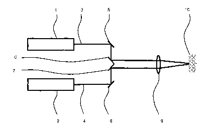
figure
9 A illustrates a microfluidic device manufactured by laser engraving the
substrate
(63) prior to bonding the top layer (64). In another example Figure 9 B
illustrates a'
microfluidic structure formed by cutting entirely through a layer (66) before
sealing
with substrates (65,67) above and below.
In another preferred embodiment of the invention the device or component to
be laser processed is machined after assembly into a multi-layered component
or
device. For example, Figure 10 illustrates channel formation in a microfluidic
device
by laser machining. In this example the top layer (69) is significantly
transparent to
the laser beam (68) and one or more of the lower layers (70) absorb
significant
amounts of the laser energy enabling the formation of internal structures such
as
vias, chambers and channels (71). Such a technique is also particularly useful
for
removing swarf, debris, and cut-out areas by using one or more of the layers
bonded
to the machined layer as a sacrificial layer and removing it after the
machining,
process. Alternatively the machining process may bond the machined layer to
its
adjacent layers, or improve the bonding of such layers, by localised melting
and
reflow induced by the laser machining process around the machined areas.
In another embodiment of the invention the device or component may
incorporate layers that act as masking components to guide the radiation onto
specific locations. This approach allows the use of larger laser beams to
create
smaller structures than normally achievable with the full beam exposure. The
use of
larger beam lasers and laser curtains may also be used to increase the
throughput of
the machining process by enabling parallel machining from the same laser beam.
Such a method also offers the advantage of decreasing the alignment
requirements
for the laser system by using a mask to provide tight tolerances. Such a
masking
system may also provide greater spatial resolution in a similar manner to
traditional
lithographic systems. Furthermore, such a masking system may also provide
manufacturing advantages if the mask is part of the manufactured component by
CA 02654453 2008-12-05
WO 2007/140537 PCT/AU2007/000802
simplifying alignment between features on a single device and between each
manufactured part. Furthermore the masking material may be used to (a) improve
the
thermal heat affected zone on the sample by conducting some of the heat away
from
the structured area, (b) protect the substrates surface from debris, and / or
(c)
support the machined structures during processing. Figure 11 depicts a mask
(71)
limiting the exposure of a material (72) to a relatively large laser beam or
curtain (73).
In another embodiment of the invention the device or component may
incorporate layers that use optical components, such as lenses, prisms or
other
refractive or diffractive features, to focus and / or redirect the radiation
onto specific
locations. This method also offers the advantage of decreasing the alignment
requirements for the laser system by using the optical components to provide
the
tight toierances required. Such optical components may provide greater spatial
resolution by focussing the radiation. In addition, such optical components
may also
provide manufacturing advantages by having the optical components as a part of
the
manufactured component and thus simplifying alignment between features on a
single device and between each manufactured part.
Figure 12 illustrates an example of optical components integrated onto a part
to focus the laser radiation. The example in Figure 12 A illustrates lenses
(74)
moulded onto the surface of a material (75) that is transparent to the laser
beam, the
focused radiation provides greater localised intensities that process a second
material (77) at a higher rate, or is above the ablation threshold, in
comparison to the
unfocussed radiation. Similarly the example of Figure 12 B shows a material
(78) that
is semi transparent to laser radiation (80) and at the high intensity points
where the
radiation is focused localised machining occurs (79).
In some embodiments of the invention, the mutilayer parts have layers
removed after the laser machining process, or after parts of the manufacturing
process. Extra layers may be used during the machining process for various
reasons,
for example to protect the surface from debris, act as a thermal conductor to
minimise the heat affected zone on the machined substrate, and support cut
out, or
free standing, structures as outline in US PCT/AU2007/000061. The layers may
also
be used during the machining process to focus or mask a beam, provide heat
conduction, or allow a secondary machining process to occur.
The example in Figure 13 illustrates protective layers being used to improve
the laser machining process. In this example the substrate (82) has two
protective.
16
CA 02654453 2008-12-05
WO 2007/140537 PCT/AU2007/000802
layers (81, 83), during the machining process all three materials are cut
entirely
through. Many machining processes cause deformation around the cut at the top
(84)
and boftom surfaces (85). By removing the outer sacrificial layers (81, 83)
the inner
substrate (82) is left with relatively clean surfaces (86, 87) and allows for
reduced
thermal damage in the surrounding area.
In one embodiment of the invention the selectively machined layer is used to
weaken the surrounding structure to form a burst valve. These burst valves can
be
made by partially machining through a layer of a multilayer device or entirely
machining through one layer and leaving a thin adjacent layer that may rupture
under
pressure. A layer can be selectively machined by using an adjacent
transparent, heat
conductive or reflective layer. Figure 14 illustrates burst valves in a
microfluidic
device fabricated by machining entirely through a layer with transparent
adjacent
layers. Figure 14 A shows an example of the formation of a burst valve (88)
between
two adjacent channels (89, 90), by laser machining (91) through substrate (92)
transparent to the laser radiation and etching an inner layer (93) leaving
only a thin
non-absorbing layer (94) of material that can be burst under pressure. Figure
14 B
illustrates a similar structure except that the burst valve is formed between
the
channel (95) and thermoformed liquid reservoir (96). For this liquid storage
example, the thin non-machined layer adjacent to, and in contact with, the
machined
layer may for example have improved barrier and chemical compatibility
properties in
comparison to the laser-absorbing layer.
In one embodiment of the invention the selectively machined layer is used to
weaken the surrounding structure to form a tearing guide. For example, Figure
15
illustrates a machined substrate (97) that provides a tearing line (98) for
packaging.
Where some of the structural layers are machined to provide a controlled
tearing line
for the user but still maintain the barrier properties of the packaging. The
dotted line
(99) down the centre of Figure 15 A represents the cross section line for the
image
shown in figure 15 B. Figure 15 B illustrates that the inner substrate (100)
is
perforated whilst the outer layers (101, 102) remain intact.
In one embodiment of the invention the selectively machined layer is used to
perforate selected layers of a multi-layer material to alter the barrier
properties of the
device. This technique provides the added advantage of allowing spatial
control of
the barrier properties on a multi-layer device such as packaging using the
same
materials and fabrication process for the entire package. In the following
example,
17
CA 02654453 2008-12-05
WO 2007/140537 PCT/AU2007/000802
shown in Figure 16, a two pack thermoformed tray (103) uses the same sealing
multilayer laminate but provides different barrier properties to each tray
(104,105)
from the machining process. The dotted line (110) down the centre of Figure 16
A
represents the cross section line for the image shown in figure 16 B. In this
example
the thermoformed tray (109) is sealed by the three laminate layers (105, 106,
107),
and the central layer (106) is perforated to alter the barrier properties to
one of the
tray containers.
18