Note: Descriptions are shown in the official language in which they were submitted.
CA 02654456 2008-11-27
WO 2007/149846 PCT/US2007/071543
OPTICALLY CONTROLLED SILICON CARBIDE AND RELATED
WIDE-BANDGAP TRANSISTORS AND THYRISTORS
BACKGROUND
Field
[002] This invention relates to advanced microelectronic (semiconductor)
devices and methods for fabricating the same, and in particular, to
microelectronic
devices containing a region of optically active material that permits the
device to be
closed with a pulse of light of one wavelength; and then opened with a pulse
of light of
a second wavelength.
BACKGROUND OF THE TECHNOLOGY
[003] The circuit shown in Fig. 1 is widely used in diverse applications where
the conversion of one voltage or current (usually DC) to a three phase AC
voltage or
current (or vice versa) is required [1]. Examples include motor drives for
electric
vehicles, industrial motors used in factories, and utility power conditioning
systems
such a static volt-ampere-reactive (SVAR) compensators and rectifiers and
invertors
used for high-voltage DC electric power transmission, two-switch and four-
switch
versions of this circuit (the "half bridge" and the "full bridge,"
respectively) are
common in power supply applications used throughout the defense and civilian
electronics industry.
CA 02654456 2008-11-27
WO 2007/149846 PCT/US2007/071543
[004] The circuit has six semiconductor switches that can be constructed in
many forms, including the bipolar junction transistor (BJT), the metal-oxide-
semiconductor field effect transistor (MOSFET), the insulated gate bipolar
transistor
(IGBT), the static induction transistor (SIT), thyristors of the silicon
controlled
rectifier (SCR) type, the gate-turn-off (GTO) type, or the static induction
type [2].
Many other variations of the above can be found in the prior art.
[005] The basic circuit building block found in Fig. 1 is the two-switch half-
bridge phase leg (see Fig. 2). Figure 2 also shows two disadvantages of this
prior art.
The first is commonly known as the "high-side gate driver" problem in which
the
upper switch S1 is electrically controlled by gate driver circuitry whose
common
connection is the load, and thus a floating gate drive is required. This
introduces
greater complexity and cost into the final system. The second problem is the
possible
introduction of incorrect gate signals which could cause improper operation of
the
half-bridge, possibly causing a failure to occur in either the circuit or the
load. The
source of these incorrect gate signals is commonly called "electromagnetic
interference" or EMI. EMI can come from many sources and can effect all
applications. But in military related systems, there is the additional threat
of
intentionally introduced EMI from enemy action. EMI can effect the operation
of any
and all switches in the circuit, including the low-side switch S2 in Fig. 2.
[006] Optically controlled circuits represent one remedy to both the high-side
gate driver problem and the EMI problem. Figure 3 illustrates another
embodiment of
the prior art that partially remedies the problem. The introduction of an
additional
circuit in the gate driver is called an optical receiver that allows a fiber
optic
connection between a central processor and any of the switches in the circuit
of Fig. 3.
The fiber optic link is generally much less vulnerable to EMI, if not immune.
2
CA 02654456 2008-11-27
WO 2007/149846 PCT/US2007/071543
Unfortunately, the problem of providing isolated electrical power to the
receiver and
the gate driver remains. And the gate driver circuitry is still potentially
vulnerable to
EMI. The former problem is especially troublesome whenever a long string of
devices
are connected in series to multiply the total blocking voltage of the stack,
as is often
the case in electric utility equipment.
[007] A typical response is to eliminate, if possible, the gate driver
circuitry
all together. The use of optically active switches is one solution. Figure 4
reveals
additional prior art in which optically active devices, usually optically
triggered
thyristors, are used because they do not need a gate driver to be switched on
or
"closed." Generally, optical radiation of a characteristic wavelength
generated by a
laser (but other sources of optical energy can be used) is conducted by
suitable means
(usually fiber optic cable) to the switch. Electron-hole pairs are generated
in the
portion of the switch that is illuminated such that the device switches into
conduction
[3]. The principal limitation is that the switch cannot usually be switched
off with
light, which accounts for the popularity of thyristors because they can
generally be
switched off by the external circuit through a process known as commutation.
This
limits the optically triggered thyristor, by far the most commonly used
optically active
switch used in power electronics, to applications where circuit commutation is
possible; however, in many applications commutation is not an option which
severely
limits the application of the prior art in optically active switches.
[008] Optically active BJTs, also known as phototransistors, are commonly
used in the microelectronics industry in devices such as "optical isolators"
(or "opto-
isolators" for short) and light detectors of various kinds and applications.
Phototransistors are rarely used in circuits like Fig. 1, but in principal
they could be.
Phototransistors of the prior art are a variation on the optically triggered
thyristor in
3
CA 02654456 2008-11-27
WO 2007/149846 PCT/US2007/071543
that electron-hole pairs are generated by a light source with a photon energy
that
exceeds the bandgap energy of the semiconductor used in the transistor. The
base of
the BJT is usually chosen to be the optically active medium. An advantage of
the
optically active BJT is that conduction through the transistor will continue
only for as
long as the light shines on the base of the BJT. When the light is removed,
the BJT
will stop conducting current and in due course the switch will turn off or
"open." The
problem is that the delay prior to switch off is generally determined by the
physics of
minority carrier storage in the base of the BJT which is generally slow for
BJTs that
have good optical gain [4]. The phototransistor can be made faster by
introducing
impurities that result in a short minority carrier lifetime (MCL) but this
negatively
impacts the optical gain. In most applications, the optical energy required to
initiate
and sustain conduction is an important figure of merit, where less is much
better.
[009] Similar problems arise in the development of semiconductor switches
intended to control large amounts of transient power, known as pulsed power
generators. These systems are generally found in defense and medical
applications.
Very fast switching is demanded by such applications [5], which has made
semiconductor device development by the pulsed power technical community
rather
distinct from that developed for applications in the conventional power
electronics
community. In the pulsed power community switches that close when illuminated
by
laser light and then open when the laser light is removed with a time constant
characteristic of the material are said to operate in the "linear mode" [6].
Linear-mode
switches can be characterized as "light-sustained" bulk photoconductive
closing and
opening switches. Such switches are similar in this respect to the
phototransistor
except that they are simpler in construction, often consisting of little more
than a block
of semiconductor, such as silicon or gallium arsenide, with a metal contact on
either
4
CA 02654456 2008-11-27
WO 2007/149846 PCT/US2007/071543
end to form Ohmic contacts for connecting the switch to the external circuit;
and their
size is typically much larger which reflects their completely different
application [7].
However, the disadvantageous trade-off in laser energy for switching speed
remains
the same [8].
[010] An alternative to the "light sustained" photoconductive switch is taught
by Schoenbach et al. in U.S. Patent 4,825,061 [9], which reveals a bulk
photoconductive device in which a laser pulse of one wavelength stimulates
persistent
photoconductivity which continues for up to many microseconds after the laser
pulse
of nanosecond duration has terminated [10]; and which can be terminated on
demand
by application of a second "quenching" laser pulse of longer wavelength [11].
Schoenbach et al. in `061 takes advantage of the optical quenching effect
which was
known by 1960 to be particularly strong in Gallium Arsenide doped with copper
[12].
The physics of infrared optical quenching in photosensitive semiconductors
like
copper-doped GaAs and CdS, the fundamental basis of `061, were adequately
understood by 1965 [13]. The teaching of Schoenbach et al. in `061 is limited
to the
use of these effects in a bulk photoconductive switch whose embodiment is
described
generally in [7] and [9] and is illustrated in Fig. 5. A substantial
literature, e.g. [14]
and [ 15], reveals that the teaching can be practically realized by a
photoconductive
switch intended for circuits like that shown in Fig. 6 and that are generally
utilized in
pulsed power applications, for example, as taught by Stoudt et al. in U.S.
Patent
5,864,166 [16]. All demonstrations of practical working devices have been
limited to
the bulk photoconductive switch taught by Schoenbach et al. in `061 and
fabricated
with the same core process of compensating silicon-doped GaAs with copper
(GaAs: Si:Cu) by thermal diffusion to make a bulk semi-insulating material
[17].
Indeed, no other practical teaching is contained in `061.
CA 02654456 2008-11-27
WO 2007/149846 PCT/US2007/071543
[011] The advantage of the GaAs:Si:Cu photoconductive switch, as compared
to the pulsed power switching prior art, is that it has high photoconductive
gain in a
material with short minority carrier lifetime, thus offering a much lower
consumption
of laser power to applications requiring current pulses with fast rise and
fall times and
a long and/or continuously variable duty ratio. However, as reported in [14]
only
relatively low average electric fields of the order of 3 kV/cm can be
controlled in
GaAs:Si:Cu bulk photoconductive switches because of a fundamental instability
that
leads to current filamentation [18], so to block large voltages and to conduct
large
currents, an extremely large active area is required with respect to the
conventional
semiconductor devices used in the power electronics industry. Therefore,
prohibitively large laser energy is required to apply the switch to power
electronics
applications. An additional disadvantage is that GaAs is generally a poor
choice for
power electronics due, among other reasons, to its low thermal conductivity.
Schoenbach et al. does not teach an embodiment that can be practically applied
to a
better choice of semiconductor for power electronics, such as silicon carbide.
SUMMARY
[012] In one aspect, the boron-related D-center is used to compensate shallow
donors in silicon carbide to produce an optically active material capable of
exhibiting
persistent photoconductivity induced by optical radiation in the yellow or
green
portion of the electromagnetic spectrum, and optical quenching of the same
persistent
photoconductivity with optical radiation of longer wavelength in the near
infrared to
red portion of the electromagnetic spectrum. All of the important polytypes of
SiC are
rendered with essentially the same properties by compensating shallow donors
with
the boron-related D-center, including but not limited to 3C, 4H, and 6H.
6
CA 02654456 2008-11-27
WO 2007/149846 PCT/US2007/071543
[013] In various embodiments, the optically active material formed by D-
center compensated SiC is incorporated into the appropriate active regions of
a variety
of microelectronic devices used in power electronics applications by selective
means.
These means include implantation of boron into silicon carbide substrate
material
and/or epitaxial material followed by the diffusion of boron resulting in the
creation of
D-centers in one-, two-, and three-dimensional device structures via high-
temperature
thermal treatment or via continued epitaxial growth.
[014] In one embodiment, the optically active material formed by D-center
compensated SiC is incorporated in the base of an optically controllable
bipolar
junction transistor (BJT).
[015] In another embodiment, the optically active material formed by D-
center compensated SiC is incorporated into the channel of optically
controllable
vertical and lateral channel junction field effect transistors (JFETs).
[016] In yet another embodiment, the optically active material formed by D-
center compensated SiC is incorporated into the channel of an optically
controllable
metal-oxide-semiconductor field effect transistor (1VIOSFET ).
[017] In yet another embodiment, the optically active material formed by D-
center compensated SiC is incorporated into the p-base of an optically
controllable
thyristor.
[018] In still another embodiment, the optically active material formed by the
D-center compensated SiC is incorporated into the channels formed in the p-
base of an
optically controllable static induction thyristor (also known as a field
controlled
thyristor).
[019] The microelectronic devices discussed above, as well as other
configurations apparent to others skilled in the art upon examination of these
7
CA 02654456 2008-11-27
WO 2007/149846 PCT/US2007/071543
teachings, can be incorporated into power electronics systems with the
advantages of
permitting pure optical control of both the closing and opening transitions of
the
switches with virtually infinite combinations of duty ratios of the closing
and opening
periods ranging from milliseconds for a single closing optical impulse to much
longer
if a regular sequence of closing optical impulses illuminate the device active
area so as
to replenish the persistent photoconductivity.
[020] Additional advantages and features will be set forth in part in the
detailed description that follows and in part will become more apparent to
those skilled
in the art upon examination of the following or upon learning of the practice
of the
invention.
BRIEF DESCRIPTION OF THE FIGURES
[021] FIG. 1 is a general illustration of the prior art in three-phase motor
drives.
[022] FIG. 2 is an illustration of the prior art in conventional half-bridge
circuits employing electrically controlled gate drivers and electrically
controlled
switches.
[023] FIG. 3 is an illustration of the prior art in conventional half-bridge
circuits employing optically controlled gate drivers and electrically
controlled
switches.
[024] FIG. 4 is an illustration of the prior art in optically controlled half-
bridge circuits employing optically stimulated or sustained switches.
[025] FIG. 5 is an illustration of the prior art in GaAs:Cu:Si photoconductive
switches (after Ref. [15]).
[026] FIG. 6 is an illustration of the application and results of using the
prior
art in GaAs:Cu:Si photoconductive switches in a pulsed power circuit (after
Ref. [15]).
8
CA 02654456 2008-11-27
WO 2007/149846 PCT/US2007/071543
[027] FIG. 7 is an illustration of the application of one or more embodiments
of the present invention in a half-bridge circuit.
[028] FIG. 8 is an illustration of the bandgap of the optically active
material
consisting of the 6H polytype of the silicon carbide semiconductor doped with
shallow
nitrogen donors and compensated with boron acceptors and boron-related D-
centers
(6H-SiC:B:N) and contained in one or more embodiments of the present
invention.
[029] FIG. 9 is an illustration of the cycle of photoconductivity possible in
an
optically active material made from SiC:B:N compensated with D-centers when
pulses
of electromagnetic radiation of two different wavelengths consecutively
illuminate the
optically active region of one or more embodiments of the present invention.
[030] FIG. 10 is a cross-sectional view of a vertical planar bipolar junction
transistor (BJT) containing an optically active region of SiC:B:N illuminated
from the
ends in accordance with an embodiment of the present invention.
[031] FIG. 11 is an illustration of the cycle of charge control possible in an
optically active material made from SiC:B:N compensated with D-centers when
laser
pulses of two different wavelengths consecutively illuminate the optically
active
region of the bipolar junction transistor illustrated in FIG. 10.
[032] FIG. 12 is a cross-sectional view of a vertical trench bipolar junction
transistor (BJT) containing an optically active region of SiC:B:N illuminated
from the
ends through lossy waveguides fabricated in the trenches in accordance with an
embodiment of the present invention.
[033] FIG. 13 is a cross-sectional view of a vertical trench bipolar junction
transistor (BJT) containing an optically active region of SiC:B:N illuminated
from the
top into lossy waveguides fabricated in the trenches in accordance with an
embodiment of the present invention.
9
CA 02654456 2008-11-27
WO 2007/149846 PCT/US2007/071543
[034] FIG. 14 is a cross-sectional view of a vertical channel junction field
effect transistor (JFET) containing an optically active region of SiC:B:N
illuminated
directly from the top in accordance with an embodiment of the present
invention.
[035] FIG. 15 is a cross-sectional view of a lateral channel metal-oxide-
semiconductor field effect transistor (MOSFET) containing an optically active
region
of SiC:B:N illuminated directly from the top in accordance with an embodiment
of the
present invention.
[036] FIG. 16 is an embodiment of the current invention in which the
optically active device shown in FIG. 14 is used to drive the gate of a
conventional
electrically gated power device.
DETAILED DESCRIPTION
[037] The present invention provides for a silicon carbide optically active
material used to create an entire class of power devices and integrated
circuits with
significant advantages in circuits requiring or benefiting from control by
pure optical
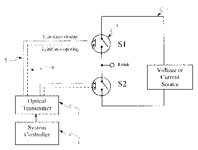
gating. An example of one such application is the circuit 1 shown in FIG. 7.
The
circuit is a half-bridge power circuit containing two transistor switches 2,
one in the
"high side" position and one in the "low side" position. A controller 3 drives
a source
of electromagnetic radiation 4 which can produce beams of electromagnetic
radiation
of one wavelength 5 and of a second wavelength 6 such that the first
wavelength is
less than the second wavelength. Both the high-side and the low-side switches
can be
illuminated with either of the beams in arbitrary sequences as determined by
the
controller. Such half-bridge circuits would have application by themselves in
various
electrical power supplies, or as output stages in integrated circuits. Or two
of them
could be connected together to form full-bridge circuits (not shown). Or three
of them
could be connected together to form three-phase circuits as illustrated in
FIG. 1. Or
CA 02654456 2008-11-27
WO 2007/149846 PCT/US2007/071543
other interconnections of these circuits could become apparent to those
skilled in the
art upon examination of the following or upon learning by practice of the
invention.
[038] The optically active material in some embodiments is based on silicon
carbide semiconductor from any of the known polytypes, the most common of
which
are 4H-SiC and 6H-SiC. However, 3C-SiC, 15R-SiC, as well as others will work
equally well. Silicon carbide is a class of semiconductors with wide bandgaps.
For
example, 4H-SiC has a bandgap of about 3.2 eV at T = 300 K, while 6H-SiC has a
bandgap of about 2.9 eV at T = 300 K. SiC is also an indirect bandgap
semiconductor.
The wide bandgap permits high-voltage and high-temperature operation at
characteristically low specific on-resistance as compared to narrow bandgap
semiconductors such as silicon or gallium arsenide. Also, SiC of any polytype
has an
advantageously large thermal conductivity (at least six times that of GaAs).
Thus, the
use of SiC devices is growing in applications requiring power semiconductor
devices,
such as the important power electronics industry.
[039] Specifically, the optically active material is SiC doped with shallow
donors, such as nitrogen or phosphorus, and compensated with boron acceptors
and
boron-related D-centers. A diagram of the bandgap 10 of an example ofthis
material
in 6H SiC is shown in FIG. 8. 6H-SiC has a conduction band 11 separated from
the
valence band 12 by an energy of 2.9 eV. The 6H-SiC material is doped during
growth
by nitrogen, which forms shallow donor levels 13 averaging 0.1 eV below the
conduction band. Either during growth, or most likely afterward, boron is
introduced
into the 6H-1-SiC. Boron forms two distinct types of impurity centers in SiC.
The
first is the boron acceptor 14 at about 0.3 eV above the valence band which is
formed
when a boron impurity atom substitutes onto a silicon vacancy site. The second
is the
D-center which forms when a boron atom substitutes onto a silicon vacancy site
that is
11
CA 02654456 2008-11-27
WO 2007/149846 PCT/US2007/071543
part of a larger complex of native point defects, such as the so-called carbon
vacancy
Vc. The D-center is definitely deeper in the bandgap than is the boron
acceptor and
any particular SiC polytype can contain concentrations of both boron acceptors
and D-
centers. The D-center has been well studied both with optical spectroscopic
means
and by thermal spectroscopic means. The result is reported as an optical
activation
energy of 0.73 eV above the valence band and a thermal activation energy
ranging
from 0.58 to 0.63 eV above the valence band [19]. FIG. 8 illustrates one
resolution of
this discrepancy by use of the two-level model found in Ref. [19] in which a D-
center
ground state 15 is located at 0.73 eV above the valence band while a second
excited
state of the D-center 16 is located at about 0.58 eV above the valence band.
The
observed difference between the optical and thermal activation energies
associated
with electron and hole capture at the D-center are predicted by this model.
The
material can be optically active when either shallow donor states outnumber
the sum
of the boron and D-center acceptor states (leaving the material n-type when in
thermal
equilibrium), or when the opposite is true (leaving the material p-type when
in thermal
equilibrium).
[040] FIG. 9 illustrates the cycle of photoconductivity that can be excited by
optically active SiC:B:N material. FIG. 9 (a) shows the equilibrium p-type
material in
its highly resistive state in which little or no conductivity is observed.
Virtually all of
the nitrogen donor states are positively charged and thus contain a trapped
hole 20.
Virtually all of the boron acceptor states and many of the D-center states are
negatively charged and thus contain a trapped electron 21. The remaining
neutral D-
center states contain a trapped hole 20.
[041] FIG. 9 (b) shows the material when illuminated by electromagnetic
energy with wavelength less than 580 nm. Photons with this energy (>2.14 eV)
will
12
CA 02654456 2008-11-27
WO 2007/149846 PCT/US2007/071543
excite process 30 in which electrons are photoionized from the D-center ground
state
15, leaving a free electron 22 and a trapped hole in the neutral D-center. As
long as
the wavelength exceeds 500 nni, there will be not be electron photoionization
of the
boron acceptor. Photons with this energy will also excite process 31 in which
trapped
holes are photoionized from the D-center ground state leaving a free hole 23
and a
trapped electron in the negatively charged D-center. Because both the B-
acceptor and
the D-center have relatively large hole capture cross sections of between 0.1
and I x
10-14 cm2 [20] free holes are likely to be trapped by both of these centers
(process 32)
where they can be excited back into the valence band by another photon
absorption
process 31. The D-center has a much smaller electron capture cross section as
revealed by D-center photoluminescence glow times of one minute at low-
temperature
[19]. Consequently, it is unlikely that a photoionized electron will be
recaptured. The
result is persistent photoconductivity (PPC), as illustrated in FIG 9 (c).
When the
source of electromagnetic radiation is removed, remaining holes in the
optically active
material are trapped by the D-center and the B acceptors through process 32.
The non-
equilibrium free electrons remain in the conduction band until either they are
captured
by the D-center (process not shown) through a characteristic emission of a
broad band
of photons centered at about 2.13 eV in 6H [20] (or 2.34 eV in 4H [21]) or
they
recombine with a hole that is thermally emitted by the D-center (process 33
followed
by process 34). The combination of processes 33 and 34 is known to occur and
is
called thermal quenching [19]. However, the time constant of the process is
governed
by the relatively slow thermal emission of holes from the D-center, which has
been
observed in numerous reports to occur on a time scale of about 10 ms at 300 K
(e.g.,
[20] and [22]). Persistent photoconductivity of this duration is about 1000
times
longer than that observed in GaAs:Cu:Si [10], and thus represents a
significant
13
CA 02654456 2008-11-27
WO 2007/149846 PCT/US2007/071543
improvement over the prior art.
[042] Persistent photoconductivity can be optically quenched as shown in
FIG 9 (d), when electromagnetic radiation with a wavelength less than 1.77 m
but
greater than 0.58 m illuminates the optically active material. Photons in
this energy
range (0.7 < hv < 2.13 eV) excite process 35 but not process 30. This means
that holes
that were being thermally emitted at a very slow rate by process 33 will now
be
emitted at a rate determined by the much greater rate of process 35. Assuming
the
recombination process 34 is of a comparable rate as hole capture by process
32, then
quenching of the PPC will occur. If the recombination process is significantly
slower
than hole capture, then optical quenching will not be observed. Therefore, the
present
invention includes an optically active material with an electron-hole
recombination
rate comparable to or faster than that of the hole capture process 32. In that
case the
material will be returned to the state shown in FIG. 9 (e), which is
substantially
similar to the initial state shown in FIG. 9 (a).
[043] FIG. 10 is an illustration of the cross section of one embodiment of
this
invention comprising a bipolar junction transistor (BJT) with an optically
active
region. The device is fabricated on an n-type conducting substrate 40. Upon
the
substrate is grown epitaxially an n-type collector 41 of sufficient thickness
and doping
to block the required voltage while the device is in the off state. Upon this
collector is
fabricated an optically active region of semiconductor 42 that acts as the
base of the
BJT. Methods for fabricating such an optically active material can be
fabricated by
compensating an epitaxial layer containing a certain concentration of shallow
donors
by introducing boron in a way that forms D-centers as disclosed in U.S. Patent
Application 2002/0149021 Al [23]. The layer 42 is sufficiently compensated
with
boron acceptors and D-centers to become highly resistive and p-type in
conductivity.
14
CA 02654456 2008-11-27
WO 2007/149846 PCT/US2007/071543
An n-type emitter layer 43 is added on top of layer 42 either by epitaxial
means or by
ion implantation. This embodiment is especially compatible with the deep mesa
edge
termination technique which is shown in FIG. 10 with a sidewall passivating
dielectric
material 46 applied Ohmic contact to the emitter layer is formed by a suitable
sequence of metal layers and heattreatments leaving a metal stack 44 as the
emitter
contact. A similar process is applied to the bottom of the substrate 40
leaving a metal
stack 45 as the collector contact. Light of one wavelength or the otheris
introduced at
the edges of the device. As the light propagates through the device from one
or more
sides, processes 30 or 35 occur in the optically active region 42 which can
change the
conductivity of this material in a way that changes the switch state of the
device. In
the case of electromagnetic radiation with a wavelength that produces process
30 the
device state is changed from non-conducting ("blocking") to conducting ("on").
In the
case of electromagnetic radiation with a wavelength that produces process 35
only, the
device state is changed from conducting ("on") to non-conducting ("blocking").
[044] The ability to activate the entire volume of optically active material
in a
power device of significant dimension is a significant advantage of this
invention. The
wavelengths of the electromagnetic radiation disclosed in the physical
description of
the photoconductivity cycle in FIG. 9 are known as sub-bandgap wavelengths
because
the photon energy of the radiation is less than the bandgap of the
semiconductor.
Therefore, the radiation is much more weakly absorbed than in the case of
above-
bandgap wavelengths. The formula for the characteristic penetration of
electromagnetic radiation into a material is given by Eq. (1):
[045] I(x) = Io exp(-a x) (1),
where I(x) is the intensity of the radiation in units of W/cm2 at a point x
inside
of the optically active materia142, Io is the initial intensity of the
radiation at the
CA 02654456 2008-11-27
WO 2007/149846 PCT/US2007/071543
surface of the BJT where the radiation is introduced into the device (x = 0),
and a is
the absorption coefficient of the radiation at the specified wavelength in
units of cm 1.
For sub-bandgap radiation, the absorption coefficient is determined by
photoionization
of deep levels, like the D-center. An approximation to the absorption
coefficient is
given by Eq. (2):
[046] a = 6ND (2),
[047] where (y is the cross section for photoionization in units of cm2 and ND
is the number density of D-centers in units of cm3. It has been reported that
a = 4.17
x 10-" cm2 for the boron-related absorption band with a threshold photon
energy of
0.7 eV [24], which is the D-center. The characteristic absorption depth of the
sub-
bandgap electromagnetic radiation is
[048] d = 1/ a. (3).
[049] The embodiment of FIG. 10, in which the electromagnetic radiation is
propagated through the length of the device, requires that d be comparable to
the
lateral dimensions of the device so that the photons are absorbed efficiently
and
uniformly throughout the optically active material. Such a large distance
means the
SiC is nearly transparent to sub-bandgap wavelengths. Typically, it is
preferable for d
> 1 mm, which means ND < 1017 cm 3.
[050] Understanding the teachings of this disclosure requires more than
simply considering the photoconductive cycle shown in FIG. 9 and the teachings
presented in `061 by Schoenbach. The incorporation of an optically active
material
into a practical semiconductor device of the type shown in FIG. 10 is not
taught in the
prior art and is a non-obvious improvement.
[051] FIG. 11 (a) illustrates one-half of a BJT of the embodiment shown in
FIG. 10. The BJT is shown with a voltage Ve applied to the collector contact
and a
16
CA 02654456 2008-11-27
WO 2007/149846 PCT/US2007/071543
voltage VE applied to the emitter contact, where Vc> VE. The optically active
material
is in the quasi-equilibrium state illustrated by FIG. 9 (a) and will thus be
partially
depleted of free holes, leaving a region of negative space charge 60.
Likewise, the n-
type material in contact with the optically active material at the
metallurgical junction
formed between the two materials is partially depleted of free electrons,
leaving a
region of positive space charge 61. The BJT in this state will allow only a
small
leakage current to flow upon application of a differential voltage VCE = VC -
VE up to
the dielectric breakdown strength of the device.
[052] FIG. 11 (b) illustrates the change in the device caused by illumination
by electromagnetic radiation with wavelength short enough to excite the
photoionization processes 30 and 31. The net result is the creation of
significant
densities of free electrons and free holes in the optically active material.
These free
carriers separate in the electric field generating an electrical current 62 by
drift and
diffusion. Electrons and holes that drift to the collector and emitter
contacts,
respectively, are replaced by new photoionization events in the optically
active
material. This gives rise to a much larger current flowing from collector to
emitter
than existed while the devices was in the blocking state shown in FIG. 11 (a).
Since
the process of photo absorption is among the fastest known to modem physics,
the
change of the BJT from the blocking state to the conducting state can occur
over the
time scale of the pulse of electromagnetic radiation, which can easily be
nothing more
than nanoseconds in duration.
[053] Eventually, the pulse of electromagnetic radiation subsides and the
remaining free holes are trapped (process 32 in FIG. 9 (b)) into boron
acceptors and
D-centers. The result is that the optically active material has been optically
converted
from an equilibrium p-type material to the non-equilibrium n-type material
illustrated
17
CA 02654456 2008-11-27
WO 2007/149846 PCT/US2007/071543
in FIG. 11 (c). The optically active material now acts like a p-base of a BJT
in which
the holes are immobile (as indeed they are because they have been trapped in
the hole
traps) so that they cannot be injected into the emitter and they cannot
recombine with
the electrons injected from the emitter 63. The loss of injected electrons is
determined
by the rate of the hole-emission process 33 in FIG. 9 (c). Since that rate is
very low
for the D-center, the device remains in the non-equilibrium state of FIG. 11
(c) for
some 10 ms at T = 300 K, and while in that state it acts as a very high-gain
BJT for
which currently there is no conventional equivalent in SiC. For conducting
current
longer than 10 ms, a second pulse of electromagnetic radiation with wavelength
sufficiently short to induce processes 30 and 31 can be applied as often as
necessary to
satisfy the desired conduction period.
[054] The persistence of the non-equilibrium conducting state shown in FIG.
11 (c) can be terminated on command at anytime by illuminating the device with
electromagnetic radiation with a wavelength sufficient to induce process 35 in
the
optically active material as shown in FIG. 11 (d). This process produces only
free
holes, which largely participate in one of three processes while in the
valence band.
One process is to be recaptured as in process 32 of FIG. 9 (b). A second is
process 64
in which the photoionized hole drifts and/or diffuses to the emitter layer,
which leaves
behind a quanta of negative space charge. A third is process 65 in which a
photoionized hole recombines with a free electron, either spontaneously or
with the
assistance of a recombination center in the bandgap of the SiC. The latter is
typically
much faster in an indirect semiconductor like SiC and thus can be expected to
dominate. In this way, minority carrier charge in the form of electrons is
rapidly
depleted from the optically active material leaving a negative space charge
region 60.
Likewise, the drift and/or diffusion of a free electron to the collector
contact in the n-
18
CA 02654456 2008-11-27
WO 2007/149846 PCT/US2007/071543
type material (process 66) that is not replaced from the optically active
material leaves
behind a quanta of positive charge; and in this way the n-type material
adjacent to the
junction is simultaneously and rapidly depleted of free electrons leaving
behind a
positive space charge region 61. Consequently, the device is returned to the
blocking
state shown in FIG. 11(e).
[055] The embodiment shown in FIG. 10 has many advantages, including the
simplicity of manufacturing the semiconductor device and the large ratio of
the active
area to the physical area of the device. One disadvantage is the problem of
propagating light efficiently and uniformly from the edges of the device
throughout
the volume of optically active material.
[056] The embodiment shown in FIG. 12 offers an improvement in this
respect. This device is also a BJT, but with a trenched cross section instead
of a planar
cross section. The device is formed on a conducting n-type substrate 40 by
epitaxially
growing an n-type drift layer 41. An n-type channel layer 47 is grown over the
drift
layer 41 followed by an emitter layer 43 that is grown or implanted onto or
into,
respectively, the channel layer. Trenches are formed such that their depth
exceeds the
thickness of the emitter layer 43. Boron is implanted into the trenches while
prevented
from being implanted into the emitter layer by a suitable masking material,
and thus
representing a self-aligned process. Such an embodiment also incorporates
teachings
found in the specification and claims of U.S. Patent 6,767,783 [25]. The boron
implanted region 48 represents a solid source of boron selectively placed into
the
trench structure. An additional thermal process step of sufficient temperature
will
cause boron to diffuse into the channel layer and introduce boron acceptors
and D-
centers, thus selectively producing a region of p-type optically active
material 42. The
trenches are filled with a combination of dielectric materials 49 that serve
two
19
CA 02654456 2008-11-27
WO 2007/149846 PCT/US2007/071543
purposes. First, the dielectric materials provide surface passivation and
electrical
insulation of the emitter base junction formed between the emitter layer and
the p-type
optically active material. The dielectric stack also forms a lossy waveguide
of
electromagnetic radiation at optical frequencies, including the infrared band
and the
visible band. To finish the device, an edge termination structure is formed,
such as the
deep mesa with dielectric passivation structure 46 illustrated. Ohmic metal
contacts
are added to form the emitter contact 44 and the collector contact 45.
[057] As shown in FIG. 12, when beams of electromagnetic radiation 36 are
launched down the trenches from one or both ends of the device, some of the
radiation
scatters into the optically active material on either side of the trench,
producing
processes 30 and 31 or process 35 depending on the wavelength of the
radiation. The
BJT is switched from the non-conducting state to the conducting state and back
to the
non-conducting state in a sequence essentially identical to that shown in FIG.
11. The
width of the channel fingers can be optimally chosen by those skilled in the
art to fall
in a range from one micrometer to many micrometers, depending on the channel
doping and the absorption length of the electromagnetic radiation.
[058] Both of the embodiments shown in FIG. 10 and FIG. 12 still require
the electromagnetic radiation to be introduced from the edges of the device,
which
increases the complexity of the interface between the device and the source of
the
electromagnetic radiation. FIG. 13 is yet another embodiment of the invention
that is
a BJT substantially similar to the embodiment shown in FIG. 12 except that the
emitter contact 44 has openings fanned such that electromagnetic radiation can
be
launched into the waveguide 49 from the top of the device. The radiation is
again
scattered into the optically active material 42 as with the embodiment shown
in FIG.
12. This, and all embodiments that are excited with electromagnetic radiation
from the
CA 02654456 2008-11-27
WO 2007/149846 PCT/US2007/071543
top, are highly compatible with many different edge termination techniques in
addition
to the deep mesa technique shown in FIG. 13, including (but not limited to)
raised and
buried guard rings and the junction termination extension (JTE) in its many
forms.
[059] Yet another embodiment modifies the BJT device structure to add a
junction field effect transistor (JFET) structure as shown in FIG. 14. The
device is
formed of a conducting substrate 40 and an n-type drift layer 41 as in
previous
devices. A layer of strongly p-type material 50 is added using a dopant other
than
boron, such as aluminum. The layer can be formed either by epitaxial means or
by
implantation. A boron implant 48 is added to the surface of the p-type layer
50.
Trenches are formed through the p-type layer and a channel is regrown using
epitaxial
means to fill the trenches and cover the p-type layer and the boron implant
using
methods that leave a substantially planar surface. On top of the channel a
heavily
doped n-type layer 43 is also grown. Such an embodiment also incorporates
teachings
found in the specification and claims of [26]. During this regrowth, boron
diffuses
into the growing channel forming boron acceptors and D-centers and converting
the
channel into a p-type optically active material 42. Ohmic metal is added to
the top of
the source layer 43 and the bottom of the substrate 40 to form source contact
44 and
drain contact 45, respectively. The source contact is patterned by
photolithographic
means to open windows to allow electromagnetic radiation to pass through the
source
layer 43 and stimulate in the optically active material 42 processes 30 and 31
or
process 35, depending on the wavelength of the radiation. This causes the
device to
switch from a non-conducting state to a conducting state and back to a non-
conducting
state similarly to that shown in FIG. 11. The source contact 44 also makes
electrical
contact with the p-type layer 50 to ensure that the potential between the
source and this
p-type layer is zero.
21
CA 02654456 2008-11-27
WO 2007/149846 PCT/US2007/071543
[060] It may be desirable in some applications for the depleted portion of the
semiconductor device at the boundary of the drift region and the optically
active
material to not be significantly illuminated by electromagnetic radiation. In
FIG. 15
yet another embodiment is illustrated in which the JFET channel region is
shorted by a
heavily n-type material 51. The conduction of current through the device is
thus
controlled solely by the conducting state of the optically active material 42
at the
surface of the device. In this embodiment, a window is opened in both the
source
contact 44 and the source layer 43. The surface of the channel between the
source
material 43 and the channel layer 51 is in contact with the dielectric
passivation
material 46. This embodiment is similar to an un-gated metal-oxide
semiconductor
field effect transistor (MOSFET). The window through the source contact and
the
source material allow the optically active material to be stimulated by
electromagnetic
radiation from the top and thus the device operates similar to the embodirnent
shown
in FIG. 14.
[061] An important consideration for determining whether the present
invention has practical application is the amount of energy in each pulse of
electromagnetic radiation required to cause the device to change conducting
state. A
kinematic approach is taken to estimate a figure of merit, which is the
optical energy
per ampere of current required.
[062] The energy per unit area is given by Eq. (4):
[063] E/A = 71 q hv ND (4),
[064] where E/A is energy per unit area in each pulse of electromagnetic
radiation in units of J/cmZ, ri is the dimensionless multiplication factor
required to
address various inefficiencies of optical excitation, q is the elementary
charge = 1.60 x
10-19 C, hv is the energy per photon in units of eV, which for 4H-SiC is
estimated to be
22
CA 02654456 2008-11-27
WO 2007/149846 PCT/US2007/071543
2.4 eV, and ND is the effective maximum number density of electrons in units
of cm 3
that can be excited into persistent photoconductivity, which is approximately
given by
the shallow donor density in the optically active material.
[065] The figure of merit is computed by normalizing Eq. (4) with the current
density to be conducted by the device while in persistent photoconductivity.
The rated
current of a typical power device is specified at a forward voltage of 2 V. If
the
specific on resistance of the device is at about the state of the art for 4H-
SiC power
JFETs, then p(Qn) = 2.5 mS2-cm2 [27]. The expected rated current density for
this
technology is
[066] J V(on) / p(on) = 2 V / 2.5 mS2-cm2 = 800 A/cm2 . (5)
[067] By normalizing Eq. (4) with Eq. (5) the figure of merit is written as:
[068] (E/A) / J = i1 q hv ND p(on) / V(an) (6)
[069] For ND =1 x 1016 cm`3 about the correct value for a 600-V device with
p(on) = 2.5 mS2-cm2, and ignoring rl for the moment, then (E/A) / J = 2 nJ/A.
The
multiplication factor rl cannot be less than 2 in a material optimized only
for turn on,
and if the efficiency is balanced for good turn off performance as well, then
the
multiplication factor may be as large as 10. The frequency of electromagnetic
pulses
that must be applied to maintain conduction depends on the thermal hole
emission
rate, which at room temperature is quite low at 100 s' [20]. But as the
junction
temperature increases, so does the rate of hole emission. At T = 200 C, the
hole
emission rate will increase about 10,000 fold and the characteristic hole
emission time
becomes about 1 s. Since the repetition frequency of the typical power
electronics
application is less than 1 MHz, then it can be assumed that in a practical
application
the time interval between pulses of electromagnetic radiation at working
temperature
is governed by the hole emission rate. A pulse repetition frequency (PRF) of 1
MHz
23
CA 02654456 2008-11-27
WO 2007/149846 PCT/US2007/071543
multiplied by the figure of merit (including an efficiency multiplier of 10)
means that
the required average power of the source of electromagnetic radiation is about
2 nJ/A
x 10 x 106 Hz = 20 mW/A. So, for example, a 100-A 4H-SiC BJT device at 200 C
requires about 2 W of optical power to sustain conduction. This is quite
practical, but
it is not insignificant.
[070] Another approach to achieve insertion into an application with the same
functionality as shown in FIG. 7 is to pair a small-scale version of a device
with the
embodiment of this invention and a full-scale power device of conventional
construction. Such a full scale conventional device might be made from silicon
carbide, or it might be made from silicon, or yet another material among the
many
semiconductors. If such a conventional device were a normally off device (a so-
called
"enhancement mode" device), then the circuit shown in FIG. 16 represents
another
embodiment of the invention because if the components revealed in FIG. 16 are
packaged together, then a device results that is essentially indistinguishable
from a
monolithic embodiment of the invention as revealed in FIGS. 10, 12, 13, 14,
and 15.
[071] In FIG. 16, the power device of conventional construction 2 can be a
BJT, an enhancement-mode MOSFET, a normally off JFET, or a gate turn-off (GTO)
thyristor, or any other similar power device. When a pulse of electromagnetic
radiation 5 illuminates an optically controlled JFET 7 of similar construction
as shown
in FIG. 14, it switches positive gate bias to the power device 2 from an
energy storage
network 8 consisting of an element that stores electrical charge and an
element that
permits the flow of current in only one direction, such as a diode. The diode
allows
the electrical storage device to be charged by the source of voltage being
switched by
the power device 2, but not to be discharged by the power device. The network
9 that
is connected between the gate and common terminal of the power device performs
two
24
CA 02654456 2008-11-27
WO 2007/149846 PCT/US2007/071543
functions. First, it limits the voltage that can be applied to the gate with
respect to the
common terminal to a safe value. In this function it is assisted by the
optically
controlled JFET 7 which is capable of self-limiting the current to the network
9 even
when the voltage across the charge storage element in network 8 is as large as
the
rated blocking voltage of the power device 2. Second, it maintains a path for
the
charge stored in the power device to be discharged from the gate to the common
terminal of the power device. One example of a network 9 is one formed by a
voltage
limiting diode, known as a Zener diode, connected in parallel with a resistor.
Alternatively, the resistor can be replaced with a device that acts like a
current source,
such as a JFET with gate and source terminals shorted together. When a pulse
of
different wavelength 6 illuminates the optically controlled JFET 7 then the
JFET turns
off and the gate of the power device 2 is discharged by the network 9 causing
the
power device to turn off. As shown in FIG. 16, the controller 3 is able to
control the
conventional power device with an optical transmitter 4 in the same way as
shown in
FIG. 7; albeit with an advantageous reduction in the optical energy required.
[072] The gain from the embodiment shown in FIG. 16 can be estimated by
considering the reduction in the size of the optically controlled device with
respect to
that of the full-scale power device. A figure of merit that describes the
power
handling capability of a power switching device is the product of the on-
resistance of
the device R( n) and the gate charge QG required to switch the device into
conduction
down to R( n). The best SiC power JFET devices have an R(( n) QG product equal
to
about 5 x 10"9 SZC at 200 C. The rated drain current of the power device is ID
= V(aõ) /
R(on). The average gate current that must be supplied by the optically
controlled device
is 1G = PRF x QG. Therefore,
[073] R'( n) QG = (V (on) / PRF) X (IG / ID) (7),
CA 02654456 2008-11-27
WO 2007/149846 PCT/US2007/071543
[074] where the optical gain is equal to the reciprocal of the ratio of the
area
of the optically controlled device to that of an equivalent optically
controlled device
equal in size to the conventional power device, which is equal to the ratio IG
/ ID.
Solving (7) for IG / ID and assuming V(an) = 2 V and PRF = 1 MHz then Io / ID
=
0.0025. The optical gain is the reciprocal of this ratio which is 400. If in
the previous
example the embodiment shown in FIG. 16 is used, then to switch the same 100 A
at
200 C the required optical power is reduced by a factor of 400 to 5 mW.
Appropriate
sources of pulsed electromagnetic radiation capable of supplying average power
of this
magnitude are easily available and relatively inexpensive.
[075] Example embodiments of the present invention have now been
described in accordance with the above advantages. It will be appreciated that
these
examples are merely illustrative of the invention. Many variations and
modifications
will be apparent to those skilled in the art.
[076] Furthermore, the purpose of the Abstract is to enable the U.S. Patent
and Trademark Office and the public generally, and especially the scientists,
engineers
and practitioners in the art who are not familiar with patent or legal terms
or
phraseology, to determine quickly from a cursory inspection the nature and
essence of
the technical disclosure of the application. The Abstract is not intended to
be limiting
as to the scope of the present invention in any way.
26
CA 02654456 2008-11-27
WO 2007/149846 PCT/US2007/071543
REFERENCE
[ 1] Philip Krein, "Chapter 1: Introduction," Power Electronics Handbook, ed.
M. H.
Rashid. Academic Press, San Diego, CA, 2001, pp. 7-8.
[2] Philip Krein, "Chapter 1: Introduction," Power Electronics Handbook, ed.
M. FL
Rashid. Academic Press, San Diego, CA, 2001, p. 10.
[3] Jerry Hudgins, Enrico Santi, Antonio Caiafa, Katherine Lengel, and Patrick
R.
Palmer, "Chapter 3: Thyristors," Power Electronics Handbook, ed. M. H. Rashid.
Academic Press, San Diego, CA, 2001, p. 44.
[4] J. Wilson and J. F. B. Hawkes, Optoelectronics: An Introduction. Prentice-
Hall
international, London, 1983, pp. 323-324.
[5] M. Buttram, "Chapter 1: Introduction," High-Power Optically Activated
Solid-
State Switches, eds. A. Rosen and F. Zutavern. Artech House, Norwood,
Massachusetts, 1994, p. 2.
[6] M. D. Pocha and W. W. Hofer, "Chapter 3: High-Speed Switching in
Photoconductors, " High-Power Optically Activated Solid-State Switches, eds.
A.
Rosen and F. Zutavern. Artech House, Norwood, Massachusetts, 1994, p. 48.
[7] Fred J. Zutavern and Guillermo M. Loubriel, "Chapter 11: High-Voltage
Lateral
Switches From Silicon or Gallium Arsenide," High-Power Optically Activated
Solid-
State Switches, eds. A. Rosen and F. Zutavern. Artech House, Norwood,
Massachusetts, 1994, pp. 247-251.
[8] K. H. Schoenbach, "Chapter 6: Optically Activated Opening of Copper-Doped
Gallium Arsenide Switches," High-Power Optically Activated Solid-State
Switches,
eds. A. Rosen and F. Zutavern. Artech House, Norwood, Massachusetts, 1994, p.
95.
[9] Karl H. Schoenbach, Rudolf K. F. Germer, Vishnukumar K. Lakdawala,
Sacharia
Albin, "Optically Controlled Bulk Semiconductor Switch Not Requiring Radiation
to
27
CA 02654456 2008-11-27
WO 2007/149846 PCT/US2007/071543
Sustain Conduction," U.S. Patent Document 4,825,061, April 1989.
[10] M. S. Mazzola, K. H. Schoenbach, V. K. Lakdawala, R. Germer, G. M.
Loubriel,
and F. J. Zutavem, "GaAs Photoconductive Closing Switches with High Dark
Resistance and Microsecond Conductivity Decay," Appl. Phys. Lett.., vol. 54,
pp. 742-
744, 1989.
[11] M. S. Mazzola, K. H. Schoenbach, V. K. Lakdawala, and S. T. Ko,
"Nanosecond
Optical Quenching of Photoconductivity in a Bulk GaAs Switch," Appl. Phys.
Lett..,
vol. 55, pp. 2102-2104, 1989.
[12] Joseph Blanc, Richard H. Bube, and Harold E. MacDonald, "Properties of
High-
Resistivity Gallium Arsenide Compensated with Diffused Copper, J. Appl. Phys.,
vol.
32, pp. 1666-1679, 1961.
[13] Jose Saura and Richard H. Bube, "Laser-Quenching of Photoconductivity and
Recombination Processes in Sensitive Photoconductors," J. Appl. Phys., vol.
36, pp.
3660-3662, 1965.
[14] Michael S. Mazzola, Karl H. Schoenbach, Vishnu K. Lakdawala, and Randy
Roush, "Infrared Quenching of Conductivity at High Electric Fields in a Bulk
Copper-
Compensated, Optically Activated GaAs Switch," IEEE Trans. Electron Dev., vol.
37,
pp. 2499-2505, 1990.
[15] David C. Stoudt, Randy A. Roush, Michael S. Mazzola, and Scott F.
Griffiths,
"Investigation of a Laser-Controlled, Copper-Doped GaAs Closing and Opening
Switch," Proc. IEEE Pulsed Power Conf., pp. 41-44, 1991.
[16] David C. Stoudt and Michael A. Richardson, "Bistable Photoconductive
Switches
Particularly Suited For Frequency-Agile, Radio-Frequency Sources," U.S. Patent
Document 5,864,166, January 1999.
[ 17] Randy A. Roush, David C. Stoudt, and Michael S. Mazzola, "Compensation
of
28
CA 02654456 2008-11-27
WO 2007/149846 PCT/US2007/071543
Shallow Silicon Donors by Deep Copper Acceptors in Gallium Arsenide,"Appl.
Phys.
Lett.., vol. 62, pp. 2670-2672, 1993.
[18] Michael S. Mazzola, Randy A. Roush, David C. Stoudt; and Scott F.
Griffiths,
"Analysis of Nonohmic Current-Voltage Characteristics in a Cu-Compensated GaAs
Photoconductor," Appl. Phys. Lett.., vol. 59, pp. 1182-1184, 1991.
[ 19] Stephen E. Saddow, C. Wesley Tipton, and Michael S. Mazzola, "Hole
Capture
by D-center Defects in 6H-Silicon Carbide," J Appl. Phys., vol. 77, pp. 318-
322,
1995.
[20] W. Suttrop, G. Pensl, and P. Lanig, "Boron-Related Deep Centers in 6H-
SiC,"
Appl. Phys. A, vol. 51, pp. 231-237,1990.
[21] Hrishikesh Das, "The Creation of Boron Deep Levels by High Temperature
Annealing of 4H-SiC," Thesis, Master of Science in Electrical Engineering,
Mississippi State University, pp. 45-46, 2004.
[22] Michael S. Mazzola, Stephen E. Saddow, Philip G. Neudeck, V. K.
Lakdawala,
and Susan We, "Observation of the D-Center in 6H-SiC p-n Diodes Grown by
Chemical Vapor Deposition," Appl. Phys. Lett., vol. 64, pp. 2370-2372, 1994.
[23] Jeffrey B. Casady and Michael S. Mazzola, U.S. Patent Application
Publication
2002/0149021 Al, October 2002.
[24] J. R. Jenny, M. Skowronski, W. C. Mitchel, H. M. Hobgood, R. C. Glass, G.
Augustine, and R. H. Hopkins, "Optical and Electrical Characterization of
Boron
Impurities in Silicon Carbide Grown by Physical Vapor Transport," J. Appl.
Phys.,
vol. 79, pp. 2326-2331, 1996.
[25] Jeffrey B. Casady, Geoffrey E. Carter, Yaroslav Koshka, Michael S.
Mazzola,
Igor Sankin, "Self-Aligned Transistor and Diode Toplogies in Silicon Carbide
Through The Use of Selective Epitaxy or Selective Implantation," U.S. Patent
29
CA 02654456 2008-11-27
WO 2007/149846 PCT/US2007/071543
Document 6,767,783, July 2004.
[26] Lin Cheng and Michael S. Mazzola, "Vertical-Trench Junction Field-Effect
Transistor Having Epitaxially Grown Drift, Buried Gate and Guard Rings, Self-
Planarized Channel and Source Regions in Silicon Carbide," Merchant & Gould
docket number 70034.O10US01.
[27] Lin Cheng, Janna Casady, Michael Mazzola, Igor Sankin, Joseph Merrett,
Volodymyr Bondarenko, Robin Kelley, Jeffery Casady, "Fast Switching (41 MHz),
2.5 m92=cm2, High Current 4H-SiC VJFETs for High Power and High Temperature
Applications," presented at Inter. Conf Silicon Carbide and Related Mat.
(ICSCRM),
Pittsburgh, Pennsylvania, 2005.