Note: Descriptions are shown in the official language in which they were submitted.
CA 02655293 2008-12-12
WO 2007/146853 PCT/US2007/070827
METHOD TO REDUCE POWER CONSUMPTION
WITH ELECTRO-OPTIC LENSES
CROSS-REFERENCE TO RELATED APPLICATIONS
[0001] This application claims the benefit of U. S. Provisional Application
No.
60/804,494, filed June 12, 2006.
BACKGROUND OF THE INVENTION
[0002] This invention relates to electro-optic lenses having reduced power
consumption.
[0003] Electra-optic devices have been developed for use in many applications,
including spectacle lenses, optical systems, liquid crystal displays and other
devices.
It is desired that the power required to drive the device be as low as
possible, to
allow long device life before recharging and to permit smaller power sources
to be
used, among other benefits.
SUMMARY OF THE INVENTION
[0004] Provided is an electro-optic device having reduced power consumption.
More specifically, an electro-optic device is provided comprising: a liquid
crystal layer
between a pair of opposing transparent substrates; a patterned electrode set
positioned between the liquid crystal layer and the inward-facing surface of
the first
transparent substrate; a conductive layer between the liquid crystal layer and
the
inward-facing surface of the second transparent substrate; and means for
applying
voltage to the patterned electrode set and the conductive layer, wherein the
voltage
applied to the conductive layer is below the threshold voltage (the RMS
voltage
difference above which the optical transmission of the liquid crystal layer
changes).
In one particular embodiment, the voltage difference between the voltage
applied to
the patterned electrode set and the voltage applied to the conductive layer is
sufficient to provide the desired amount of optical transmission change in the
liquid
crystal.
[0005] As known in the art, substantially homogenously aligned liquid crystals
have
a surface anchoring energy and significant elastic constants that result in no
director
1
CA 02655293 2008-12-12
WO 2007/146853 PCT/US2007/070827
reorientation at RMS voltages below a threshold level (Vm). If the RMS voltage
applied across the liquid crystal is higher than VTh, the director reorients
and the
optical transmission changes until saturation is reached. In previous designs,
to
reorient the liquid crystal, a voltage was applied across the liquid crystal
using the
conductive layer as a ground. This applied voltage was at least the sum of the
threshold voltage and the additional amount of voltage to reorient the
director to the
desired extent. In this invention, the conductive layer (unpatterned
electrode) is
driven near the threshold voltage. This allows the patterned electrode to be
driven at
a lower voltage than in previous designs.
[0006] In one example of the current invention, the threshold voltage is about
1.3 V
RMS. In this case, a voltage below 1.3 V RMS is applied to the conductive
layer.
The voltage applied to the patterned electrodes is sufficient such that the
liquid
crystal director reorients to provide the desired optical transmission. This
voltage is
less than in previous designs.
[0007] The devices of the invention can be used in a variety of applications
known
in the art, including lenses used for human or animal vision correction or
modification. The lenses can be incorporated in spectacles, as known in the
art.
Spectacles can include one lens or more than one lens. The devices may also be
used in display applications, as known to one of ordinary skill in the art
without
undue experimentation. The lenses of the invention can be used with
conventional
lenses and optics.
[0008] The devices of this invention offer many advantages over other designs.
Previous work indicated that the electronic drivers that drive the liquid
crystal
consume the majority of the power supply's energy. The use of this invention
reduces the power consumed by the electronics that drive the liquid crystal.
With the
use of this invention, lower voltage power supplies can be used. Since the
devices
described herein may be used as components of eyewear, where the power supply
can be a battery, a lower voltage power supply will allow the use of a smaller
battery,
and reduced power consumption will extend the time between battery charges.
2
CA 02655293 2008-12-12
WO 2007/146853 PCT/US2007/070827
BRIEF DESCRIPTION OF THE FIGURES
[0009] Figure 1 shows an illustration of a liquid crystal cell.
[0010] Figure 2 shows the previous design where a voltage is applied across a
liquid crystal cell.
[0011] Figure 3 shows one example of a patterned electrode set.
[0012] Figure 4 shows the use of oppositely phased square-wave drivers.
DETAILED DESCRIPTION OF THE INVENTION
[0013] The following description provides non-limiting details of constructing
the
electro-optic lenses of the present invention. This invention provides electro-
optic
lenses filled with liquid crystal material that can be realigned in an
electric field. The
lenses function as diffractive-optical-elements (DOE). DOE are the result of
applying
voltages across a thin liquid-crystal layer which responds by altering the
director-
orientation field and creates nonuniform refractive-index patterns which then
lead to
a nonuniform phase-transmission-function (PTF) across the face of the cell.
Accurate control of the PTF to create the desired DOE is achieved by applying
an
accurately controlled voltage difference across the cell by driving the
patterned
electrode set and the conductive layer.
[0014] The electro-optic lens used in the present invention is a diffractive
lens using
a patterned electrode set to produce the desired distribution of phase
retardations
that allows the lens to function as a zone-plate lens. Diffractive lenses are
known in
the art. The function of a diffractive lens is based on near-field diffraction
by a
Fresnel zone pattern. Each point emerging from the structure serves as an
emitter
of a spherical wave. The optical field at a particular observing point is a
summation
of the contributions of the emitted spherical waves over the entire structure.
Constructive interference of the spherical waves coming from the various
points
creates a high intensity at the observation point, corresponding to a high
diffraction
efficiency.
3
CA 02655293 2014-08-27
[0015] Liquid crystal cells are known in the art.
As one example, consider an electro-
active liquid crystal cell, as shown in Figure 1, where liquid crystal
material (20) is
sandwiched between two substrates (100, 10) that have conductive inner
surfaces
(40, 30). The substrates can be any material that can provide desired optical
transmission and can function in the devices and methods described herein,
such as
quartz, glass or plastic, as known in the art. Conductive layer 30 is
patterned with a
patterned electrode set to provide the desired diffraction pattern. The
patterned
electrodes consist of a circular array of rings whose radii are determined by
the focal
length desired, as described elsewhere (see for example, references cited
herein
and US application 2004/0223113). The patterned electrode is fabricated by
photolithographic processing of a conductive film deposited on a substrate, or
other
techniques, as known in the art. Figure 3 illustrates the layout of one
example of an
electrode pattern. Adjacent zones are distinguished by grey and black colors.
Each
ring electrode is independently addressable by adding an electrical insulation
layer
with vias (represented by dots). Conductive layer 40 is not patterned. The
conductive material used for the conductive layers may be any suitable
material,
including those specifically described herein, and other materials known in
the art. It
is preferred that the conductive material be transparent, such as indium
oxide, tin
oxide or indium tin oxide (ITO). The thickness of each conducting layer is
typically
between 30 nm and 200 nm. The layer must be thick enough to provide adequate
conduction, but not so thick as to provide excess thickness to the overall
lens
structure. The substrates are kept at a desired distance with spacers (60), or
other
means known in the art. Spacers may be any desired material such as Mylar,
glass
or quartz, or other materials useful to provide the desired spacing. In order
to
achieve efficient diffraction the liquid crystal layer must be thick enough to
provide
one wave of activated retardation (d > A / On ¨ 2.5 pm, where On is the
birefringence
of the liquid crystal media), but thicker liquid crystal layers help to avoid
saturation
phenomena. Disadvantages of thicker cells include long switching times
(varying as
d2) and loss of electro-optic feature definition. In particular embodiments,
the
transparent substrates are spaced between three and 20 microns apart, and all
individual values and ranges therein. One currently preferred spacing is 5
microns.
The surfaces of the substrates are coated with an alignment layer (50), such
as
4
CA 02655293 2008-12-12
WO 2007/146853 PCT/US2007/070827
polyvinylalcohol (PVA) or nylon 6,6 and are treated by rubbing to give a
homogeneous director orientation. It is preferred that the alignment layer on
one
substrate is rubbed antiparallel from the alignment layer on the other
substrate as
shown by the arrows in Figure 2. This allows proper alignment of the liquid
crystal,
as known in the art.
[0016] Voltage is applied to the patterned electrode set and conductive layer
using
means known in the art. In previous lens configurations, a voltage is applied
to the
inner conductive surfaces of the substrates as shown in Figure 2. The symbols
used
in Figure 2 are conventional in the art. In the previous lens configurations,
one
conductive layer served as a ground. In one embodiment of the present
invention,
one driver circuit is attached to the conductive layer and a separate driver
circuit is
attached to the patterned electrode set. Electrical contacts can be made to
the
electrodes using thin wires or conductive strips at the edge of the lens, or
by a set of
conducting vias down the lens, as known in the art. The voltages supplied to
the
conductive layer and patterned electrode set are dependent on the particular
liquid
crystal used, the thickness of the liquid crystal in the cell, the desired
optical
transmission, and other factors, as known in the art. The actual voltages used
can
be determined by one of ordinary skill in the art without undue
experimentation using
the knowledge of the art and the disclosure herein. It is known in the art
that various
methods of controlling all aspects of the voltage applied to electrodes can be
used,
including a processor, a microprocessor, an integrated circuit, and a computer
chip.
[0017] Since voltages are not absolute physical quantities, they must be
specified
relative to a reference (e.g. a local ground, a battery electrode or a power-
supply
terminal). Thus the voltage that alters the stress on and strain in a liquid
crystal (LC)
film is actually determined by the difference between voltages at the
electrodes on
opposing sides of the film. It is well known that LC films respond slowly (at
low
frequencies) to the RMS average of the higher-frequency variations (written as
< V2
>Y2) of these voltage differences. To control such films commonly one
electrode is
kept at fixed voltage V2 = Vref (e.g. at local ground). In that case the
modulating
voltage Vrms is determined completely by the behavior of voltage V1 on the
other
electrode:
CA 02655293 2008-12-12
WO 2007/146853 PCT/US2007/070827
Vrms = <(V1 ¨V2)2 >V2= < (Vi ¨ Vref)2 >1/2 = <(V1)2 >Y2
if voltages are expressed relative to Vref. However, when V2 is not held at
Vref, then
one can only say that
Vrms = < (V1¨ V2)2 >1/2 .
[0018] In that case synchronization of electrode drive voltages can cause the
values
of Vrms to occur in the range
Vrms1 + Vrms2 =?,- Vrms =?: IVrms1 - Vrms2I =
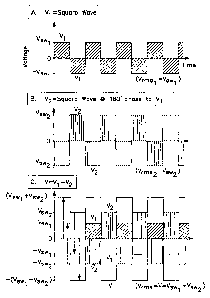
[0019] An important example, the use of oppositely phased square-wave drives
to
provide a large modulating Vrms from two lower-voltage drivers, is shown in
the
accompanying Figure 4. Obviously V2 can be kept constant as a square-wave with
amplitude Vsw2 and V1 can be applied as a square wave that is 180 degrees out-
of-
phase with respect to V2 that can be varied in amplitude Vswi to achieve the
desired
controlling voltage. For this situation, as shown in Figure 4,
Vrms = Vrmsl Vrms2 = Vsw1 Vsw2 =
[0020] So, as mentioned herein, if Vrms2 = Vsw2 is set near but below the LC
film's
threshold voltage, then smaller Vrms1 = Vsw1 values can be used to control a
LC DOE.
(An alternative would be to fix Vsw1 and to vary the phase difference between
the
square waves to achieve the desired Vrms within the range
Vswi + Vsw2 =?=: Vrms ?-' IVsw1 ¨ Vsw2I .)
[0021] Use of square waves is illustrative, but is only a simple example.
Similar
control of Vrms can be achieved through control of amplitude and phase with
other
drive wave-forms (e.g. sine waves, imperfect square waves and other methods
known in the art.).
6
CA 02655293 2008-12-12
WO 2007/146853 PCT/US2007/070827
[0022] As used herein, "layer" does not require a perfectly uniform film. Some
uneven thicknesses, cracks or other imperfections may be present, as long as
the
layer performs its intended purpose, as described herein. As used herein, a
"patterned electrode set" means one or more areas of conductive material
arranged
in a pattern on a substrate, along with one or more areas of insulating
material
arranged in a complementary pattern with said areas of conductive material on
said
substrate.
[0023] The liquid crystal used in the invention include those that form
nematic,
smectic, or cholesteric phases that possess a long-range orientational order
that can
be controlled with an electric field. It is preferred that the liquid crystal
have a wide
nematic temperature range, easy alignability, low threshold voltage, large
electro-
optic response and fast switching speeds, as well as proven stability and
reliable
commercial availability. In one preferred embodiment, E7 (a nematic liquid
crystal
mixture of cyanobiphenyls and cyanoterphenyls sold by Merck) is used. Examples
of other nematic liquid crystals that can be used in the invention are: pentyl-
cyano-
biphenyl (5CB), (n-octyloxy)-4-cyanobiphenyl (80CB). Other examples of liquid
crystals that can be used in the invention are the n =3, 4, 5, 6, 7, 8, 9, of
the
compounds 4-cyano-4-n-alkylbiphenyls, 4-n-pentyloxy-biphenyl, 4-cyano-4"-n-
alkyl-
p-terphenyls, and commercial mixtures such as E36, E46, and the ZLI-series
made
by BDH (British Drug House)-Merck.
[0024] Electroactive polymers can also be used in the invention. Electroactive
polymers include any transparent optical polymeric material such as those
disclosed
in "Physical Properties of Polymers Handbook" by J. E. Mark, American
Institute of
Physics, Woodburry, N.Y., 1996, containing molecules having unsymmetrical
polarized conjugated p electrons between a donor and an acceptor group
(referred
to as a chromophore) such as those disclosed in "Organic Nonlinear Optical
Materials" by Ch. Bosshard et al., Gordon and Breach Publishers, Amsterdam,
1995.
Examples of polymers are as follows: polystyrene, polycarbonate,
polymethylmethacrylate, polyvinylcarbazole, polyimide, polysilane. Examples of
chromophores are: paranitroaniline (PNA), disperse red 1 (DR 1), 3-methy1-4-
methoxy-4'-nitrostilbene, diethylaminonitrostilbene (DANS), diethyl-thio-
barbituric
acid. Electroactive polymers can be produced by: a) following a guest/host
7
CA 02655293 2008-12-12
WO 2007/146853 PCT/US2007/070827
approach, b) by covalent incorporation of the chromophore into the polymer
(pendant
and main-chain), and/or c) by lattice hardening approaches such as cross-
linking, as
known in the art.
[0025] Polymer liquid crystals (PLCs) may also be used in the invention.
Polymer
liquid crystals are also sometimes referred to as liquid crystalline polymers,
low
molecular mass liquid crystals, self-reinforcing polymers, in situ-composites,
and/or
molecular composites. PLCs are copolymers that contain simultaneously
relatively
rigid and flexible sequences such as those disclosed in "Liquid Crystalline
Polymers:
From Structures to Applications" by W. Brostow; edited by A. A. Collyer,
Elsevier,
New-York-London, 1992, Chapter 1. Examples of PLCs are: polymethacrylate
comprising 4-cyanophenyl benzoate side group and other similar compounds.
[0026] Polymer dispersed liquid crystals (PDLCs) may also be used in the
invention. PDLCs consist of dispersions of liquid crystal droplets in a
polymer matrix.
These materials can be made in several ways: (i) by nematic curvilinear
aligned
phases (NCAP), by thermally induced phase separation (TIPS), solvent-induced
phase separation (SIPS), and polymerization-induced phase separation (PIPS),
as
known in the art. Examples of PDLCs are: mixtures of liquid crystal E7 (BDH-
Merck)
and N0A65 (Norland products, Inc. NJ); mixtures of E44 (BDH-Merck) and
polymethylmethacrylate (PMMA); mixtures of E49 (BDH-Merck) and PMMA; mixture
of the monomer dipentaerythrol hydroxy penta acrylate, liquid crystal E7, N-
vinylpyrrolidone, N-phenylglycine, and the dye Rose Bengal.
[0027] Polymer-stabilized liquid crystals (PSLCs) can also be used in the
invention.
PSLCs are materials that consist of a liquid crystal in a polymer network in
which the
polymer constitutes less than 10% by weight of the liquid crystal. A
photopolymerizable monomer is mixed together with a liquid crystal and an UV
polymerization initiator. After the liquid crystal is aligned, the
polymerization of the
monomer is initiated typically by UV exposure and the resulting polymer
creates a
network that stabilizes the liquid crystal. For examples of PSLCs, see, for
instance:
C. M. Hudson et al. Optical Studies of An isotropic Networks in Polymer-
Stabilized
Liquid Crystals, Journal of the Society for Information Display, vol. 5/3,1-5,
(1997), G.
P. Wiederrecht et al, Photorefractivity in Polymer-Stabilized Nematic Liquid
Crystals,
J. of Am. Chem. Soc., 120,3231-3236 (1998).
8
CA 02655293 2008-12-12
WO 2007/146853 PCT/US2007/070827
[0028] Self-assembled nonlinear supramolecular structures may also be used in
the
invention. Self-assembled nonlinear supramolecular structures include
electroactive
asymmetric organic films, which can be fabricated using the following
approaches:
Langmuir-Blodgett films, alternating polyelectrolyte deposition
(polyanion/polycation)
from aqueous solutions, molecular beam epitaxy methods, sequential synthesis
by
covalent coupling reactions (for example: organotrichlorosilane-based self-
assembled multilayer deposition). These techniques usually lead to thin films
having
a thickness of less than about 1 pm.
[0029] Every device or combination of components described or exemplified can
be
used to practice the invention, unless otherwise stated. Additional components
such
as drivers to apply the voltages used, controllers for the voltages and any
additional
required optical components are known to one of ordinary skill in the art and
incorporated without undue experimentation. Specific names of compounds are
intended to be exemplary, as it is known that one of ordinary skill in the art
can name
the same compounds differently.
[0030] When a compound is described herein such that a particular isomer or
enantiomer of the compound is not specified, for example, in a formula or in a
chemical name, that description is intended to include each isomers and
enantiomer
of the compound described individual or in any combination. One of ordinary
skill in
the art will appreciate that methods, device elements, starting materials, and
fabrication methods other than those specifically exemplified can be employed
in the
practice of the invention without resort to undue experimentation. All art-
known
functional equivalents, of any such methods, device elements, starting
materials, and
fabrication methods are intended to be included in this invention. Whenever a
range
is given in the specification, for example, a thickness range or a voltage
range, all
intermediate ranges and subranges, as well as all individual values included
in the
ranges given are intended to be included in the disclosure.
[0031] As used herein, "comprising" is synonymous with "including,"
"containing," or
"characterized by," and is inclusive or open-ended and does not exclude
additional,
unrecited elements or method steps. As used herein, "consisting of' excludes
any
element, step, or ingredient not specified in the claim element. As used
herein,
"consisting essentially of" does not exclude materials or steps that do not
materially
9
CA 02655293 2014-08-27
affect the basic and novel characteristics of the claim. Any recitation herein
of the
term "comprising", particularly in a description of components of a
composition or in
a description of elements of a device, is understood to encompass those
compositions and methods consisting essentially of and consisting of the
recited
components or elements. The invention illustratively described herein suitably
may
be practiced in the absence of any element or elements, limitation or
limitations
which is not specifically disclosed herein.
[00321 The terms and expressions which have been employed are used as terms of
description and not of limitation, and there is no intention in the use of
such terms
and expressions of excluding any equivalents of the features shown and
described
or portions thereof, but it is recognized that various modifications are
possible within
the scope of the invention claimed and described. Thus, it should be
understood that
although the present invention has been specifically disclosed by preferred
embodiments and optional features, modification and variation of the concepts
herein disclosed may be resorted to by those skilled in the art, and that such
modifications and variations are considered to be within the scope of this
invention.
[0033] In general the terms and phrases used herein have their art-recognized
meaning, which can be found by reference to standard texts, journal references
and
contexts known to those skilled in the art. Specific definitions are provided
to clarify
their specific use in the context of the invention. All patents and
publications
mentioned in the specification are indicative of the levels of skill of those
skilled in
the art to which the invention pertains.
[0034] One skilled in the art would readily appreciate that the present
invention is
well adapted to carry out the objects and obtain the ends and advantages
mentioned, as well as those inherent therein. The devices and methods and
accessory methods described herein as presently representative of preferred
embodiments are exemplary and are not intended as limitations on the scope of
the
invention.
CA 02655293 2014-08-27
[0035]
[0036] Although the description herein contains many specificities, these
should not
be construed as limiting the scope of the invention, but merely providing
examples of
some of the presently preferred embodiments of the invention. The invention is
not
limited in use to spectacles. Rather, as known by one of ordinary skill in the
art, the
invention is useful in other fields such as telecommunications, optical
switches and
medical devices. Any liquid crystal or mixture of liquid crystals that
provides the
desired phase transmission function at the desired wavelength is useful in the
invention, as known by one of ordinary skill in the art. Determining the
proper
voltage and applying the proper voltage to liquid crystal materials to produce
a
desired phase transmission function is known in the art.
11
CA 02655293 2008-12-12
WO 2007/146853 PCT/US2007/070827
REFERENCES
G. Smith et al., The eye and visual optical instruments, Cambridge University
Press,
1997.
G. Vdovin et al., On the possibility of intraocular adaptive optics, Opt.
Express
11:810-817, 2003.
G. Williams et al., Electrically controllable liquid crystal Fresnel lens,
Proc. SPIE
1168:352-357, 1989.
J. S. Patel et al., Electrically controlled polarization-independent liquid-
crystal
Fresnel lens arrays, Opt. Lett. 16:532-534, 1991.
B. Dance, Liquid crystal used in switchable Fresnel lens, Laser Focus World
28:34,
1992.
M. C. K. Wiltshire, Non-display applications of liquid crystal devices, Geo J.
Research 10:119-125, 1993.
H. Ren et al., Tunable Fresnel lens using nanoscale polymer-dispersed liquid
crystals, Appl. Phys. Lett. 83:1515-1517, 2003.
C. W. Fowler et al., Liquid crystal lens review, Ophthal. Physiol. Opt. 10:186-
194,
1990.
J. A. Futhey, Diffractive bifocal intraocular lens, Proc. SPIE 1052:142-149,
1989.
S. Sato et al., Variable-focus liquid crystal Fresnel lens, Jpn. J. Appl.
Phys. 24:L626-
L628, 1985.
L. G. Commander et al., Variable focal length microlenses, Opt. Commun.
177:157-
170, 2000.
S. T. Kowel et al., Focusing by electrical modulation of refraction in a
liquid crystal
cell, Appl. Opt. 23:278-289, 1984.
A. Nouhi et al., Adaptive spherical lens, Appl. Opt. 23:2774-2777, 1984.
A. F. Naumov et al., Liquid-crystal adaptive lenses with modal control, Opt.
Lett.
23:992-994, 1998.
M. Y. Loktev et al., Wave front control systems based on modal liquid crystal
lenses,
Rev. Sci. lnstrum. 71:3190-3297, 2000.
12
CA 02655293 2008-12-12
WO 2007/146853 PCT/US2007/070827
N. A. Riza et al., Three-terminal adaptive nematic liquid-crystal lens device,
Opt.
Lett. 19:1013-1015, 1994.
P. W. McOwan et al., A switchable liquid crystal binary Gabor lens, Opt.
Commun.
103:189-193, 1993.
S. Masuda et al., Liquid-crystal microlens with a beam-steering function,
Appl. Opt.
36:4772-4778, 1997.
B. Kress et al., Digital Diffractive Optics, John Wiley & Sons Ltd., 2000.
13