Language selection

Search

Patent 2655390 Summary

Third-party information liability

Some of the information on this Web page has been provided by external sources. The Government of Canada is not responsible for the accuracy, reliability or currency of the information supplied by external sources. Users wishing to rely upon this information should consult directly with the source of the information. Content provided by external sources is not subject to official languages, privacy and accessibility requirements.

Claims and Abstract availability

Any discrepancies in the text and image of the Claims and Abstract are due to differing posting times. Text of the Claims and Abstract are posted:

  • At the time the application is open to public inspection;
  • At the time of issue of the patent (grant).
(12) Patent: (11) CA 2655390
(54) English Title: MEMS-BASED MICRO AND NANO GRIPPERS WITH TWO-AXIS FORCE SENSORS
(54) French Title: MICRO-PINCES ET NANO-PINCES A MEMS MUNIES DE CAPTEURS DE FORCES A DEUX AXES
Status: Expired and beyond the Period of Reversal
Bibliographic Data
(51) International Patent Classification (IPC):
  • B81C 01/00 (2006.01)
  • B81B 03/00 (2006.01)
  • B82B 03/00 (2006.01)
(72) Inventors :
  • KIM, KEEKYOUNG (Canada)
  • SUN, YU (Canada)
(73) Owners :
  • KEEKYOUNG KIM
  • YU SUN
(71) Applicants :
  • KEEKYOUNG KIM (Canada)
  • YU SUN (Canada)
(74) Agent: MILLER THOMSON LLP
(74) Associate agent:
(45) Issued: 2016-05-10
(86) PCT Filing Date: 2007-06-21
(87) Open to Public Inspection: 2007-12-27
Examination requested: 2012-06-20
Availability of licence: N/A
Dedicated to the Public: N/A
(25) Language of filing: English

Patent Cooperation Treaty (PCT): Yes
(86) PCT Filing Number: 2655390/
(87) International Publication Number: CA2007001090
(85) National Entry: 2008-12-16

(30) Application Priority Data:
Application No. Country/Territory Date
2,551,191 (Canada) 2006-06-23

Abstracts

English Abstract

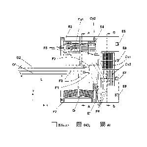
The present invention relates to a design and microfabrication method for microgrippers that are capable of grasping micro and nano objects of a large range of sizes and two-axis force sensing capabilities. Gripping motion is produced by one or more electrothermal actuators. Integrated force sensors along x and y directions enable the measurement of gripping forces as well as the forces applied at the end of microgripper arms along the normal direction, both with a resolution down to nanoNewton. The microfabrication method enables monolithic integration of the actuators and the force sensors.


French Abstract

La présente invention concerne un concept et un procédé de microfabrication de micro-pinces qui sont capables de saisir des micro-objets et des nano-objets dans une grande plage de tailles et disposant de fonctions de détection de force dans deux axes. Le mouvement de préhension est produit par un ou plusieurs actionneurs électrothermiques. Des capteurs de force intégrés dans les directions x et y permettent de mesurer les forces de préhension ainsi que les forces appliquées à l'extrémité des bras des micro-pinces dans la direction normale, avec une résolution de l'ordre du nanoNewton. Le procédé de microfabrication permet l'intégration monolithique des actionneurs et des détecteurs de force.

Claims

Note: Claims are shown in the official language in which they were submitted.


-8-
CLAIMS
What is claimed is:
1. A gripping device fabricated by a microfabrication process incorporating
photolithography masking being operable to grasp objects varying from micro
to nanoNewton, and having two-axis force sensing capabilities, comprising:
(a) two or more gripper arms including at least one driving arm and at
least one sensing arm operable together to grasp any of the objects;
(b) one or more microactuators connected to at least one of the two or
more gripper arms and operable to deform and deflect the two or more
gripper arms and to drive the at least one driving arm; and
(c) one or more force sensors connected to one or more of the two or more
gripper arms including the at least one sensing arm, said one or more
force sensors being operable with the at least one sensing arm and the
at least one driving arm so that the one or more force sensors enable
force sensing along two axes operable to measure gripping forces and
forces applied at the end of the two or more gripper arms to a
nanoNewton resolution, said axes include: (i) a longitudinal x-
directional axis so that the gripping device is operable to generate force
feedback relating to the at least one sensing arm and the at least one
driving arm grasping any of the objects, said force feedback indicating
detection of contact of the two or more gripping arms with any of the
objects as contact feedback and tensile strength and adhesion force as
gripping feedback, said force feedback being utilized by the gripping
device to avoid breakage of the two or more gripper arms; and (ii) a
lateral y-directional axis so that the gripping device is operable to
generate displacement feedback relating to deformation and deflection
of any of the two or more gripper arms; and
(d) an insulator wafer handle layer connecting the two or more gripper
arms to mechanically connect and electrically insulate the two or more gripper
arms for operation in an aqueous environment.

-9-
2. The gripping device of claim 1 further characterised in that one or more
of the
microactuators are bent-beam electrothermal microactuators, U-beam
electrothermal microactuators, or electrostatic microactuators.
3. The gripping device of claim 1 further characterised in that the force
sensors
are two-axis capacitive force sensors or piezoresistive force sensors.
4. The gripping device of claim 1 further characterised in that the force
sensors
are transverse differential capacitive comb drives.
5. The gripping device of claim 1 further characterised in that the gripper
arms
are connected to the microactuators by flexures.
6. The gripping device of claim 1 further characterised in that the gripper
arms
are connected to the force sensors by flexures.
7. The gripping device of claim 1 further characterised in that it is
operable to
grasp objects ranging from 1 nanometer to 500 microns.
8. The gripping device of claim 1 further characterised in that it is
operable to
measure the tensile strength or adhesion force of micro and nano objects by
gripping and pulling.
9. The gripping device of claim 1 further characterised in that cross-axis
coupling between two-axis force feedback is minimized.
10. The gripping device of claim 1 further characterised in that a silicon
on
insulator base material achieves electrical signal isolation between actuation
paths and sensing paths.
11. The gripping device of claim 1 further characterized in that the
gripping
device further comprises capacitance readout circuits and a tethering spring
of
dimensions operable to resolve forces down to pico-Newtons.
12. A microgripping device operable to grasp objects varying from micro to
nanoNewton and having two-axes force sensing capabilities, characterised in
that the microgripping device comprises:

-10-
(a) two or more gripper arms including at least one driving arm and at
least one sensing arm operable together to grasp any of the objects;
(b) one or more bent-beam electrothermal microactuators connected to the
at least one of the gripper arms, said bent-beam electrothermal
microactuators being operable to deform and deflect the two or more
gripper arms and to drive the at least one driving arm;
(c) one or more force sensors that are transverse differential capacitive
comb drives operable to sense force enabling contact feedback and
gripping feedback, said one or more force sensors being connected to
the one or more of the two or more gripper arms including the at least
one sensing arm, said one or more force sensors being operable with
the at least one sensing arm and the at least one driving arm so that the
one or more force sensors enable force sensing along two axes
operable to measure gripping forces and forces applied at the end of
the two or more gripper arms to a nanoNewton reolution, said axes
include: (i) a longitudinal x-directional axis so that the gripping device
is operable to generate force feedback relating to the at least one
sensing arm and the at least one driving arm grasping any of the
objects, said force feedback indicating detection of contact of the two
or more gripping arms with any of the objects as contact feedback and
tensile strength and adhesion force as gripping feedback, said force
feedback being utilized by the gripping device to avoid breakage of the
two or more gripper arms; and (ii) a lateral y-directional axis so that
the gripping device is operable to generate displacement feedback
relating to deformation and deflection of any of the two or more
gripper arms; and
(d) flexures connecting the microactuators with the gripper arms and
connecting the force sensors with the gripper arms.

Description

Note: Descriptions are shown in the official language in which they were submitted.


CA 02655390 2008-12-16
WO 2007/147239 PCT/CA2007/001090
1
MEMS-BASED MICRO AND NANO GRIPPERS WITH TWO-AXIS FORCE
SENSORS
Priority
This application claims the benefit of Canadian Patent No. 2,551,191, filed 23
June
2006.
Field of the Invention
The present invention i-elates to mici-o and nanosystems, and nlici-o and
nanotechnology.
Background of the Invention
Intelligent manipulation (e.g., grasping/gripping) of micro- and nanometer-
sized
objects requires the use of miniaturized microgrippers with integrated force
sensors.
Currently, micro- and nanomanipulation typically relies purely on visual
feedback
either from an optical niicroscope or an electron microscope. The lack of
force
feedback at the microNewton and nanoNewton level severely limits intelligent
micro-
and nanomanipulation.
Besides miniaturization and electrical control, microgrippers must be capable
of
providing multi-axis force feedback to satisfy the following requirements: (i)
to
protect the microgripper and detect the contact between the microgripper and
the
object to be nianipulated; and (ii) to provide gripping force feedback during
grasping
to obtain secured grasping while protecting the object to be grasped.
The vast majority of existing microgrippers lack force feedback due to the
difficulty
of integrating force sensors with microgrippers. The lack of force feedback
does not
perniit force-controlled manipulation and easily causes breakage of
microgrippers and
damage to the object to be manipulated.
A recently reported electrothermally driven microgripper design is integrated
with a
single-axis piezoresistive force sensor that is only capable of measuring
gripping
forces. (See K. Molhave and O. Hansen, "Electrothermally actuated
microgrippers
with integrated force-feedback," J. of Micromechanics and Microengineering,
15(6),
pp. 1265-1270, 2005.) However, the gripping force sensing resolution is
soniewhat

CA 02655390 2008-12-16
WO 2007/147239 PCT/CA2007/001090
2
poor, on the order of milli-Newton that is orders of magnitude worse than what
micro-
nanomanipulation requires.
A recent paper reports a design of an electrostatically driven nlicrogripper
with a
single-axis capacitive force sensor that is only capable of measuring gripping
forces.
(See F. Beyeler, D.J. Bell, B.J. Nelson, Yu Sun, A. Neild, S. Oberti, and J.
Dual,
"Design of a micro-gripper and an ultrasonic manipulator for handling micron
sized
objects," IEEE/RSJ International Conference on Intelligent Robots and Systems,
Beijing, China, October, 2006.) Due to the limitation of electrostatic
actuation (low
force output, small displacements, and high driving voltage), the microgripper
design
is only capable of grasping objects of a small range of sizes.
The lack of force sensing capabilities along a second-axis down to nanoNewton
in
existing designs does not allow for the protection of microgrippers and the
detection
of contact between the microgripper and object to be manipulated. What is
needed is
design and microfabrication of microgrippers that are capable of grasping
micro and
nano objects of a large range of sizes and having two-axis force sensing
capabilities.
Summary of the Invention
In one aspect, the present invention employs MEMS (microelectromechanical
systems) technology in the design and microfabrication of microgrippers that
are
capable of grasping micro and nano objects of a large range of sizes and two-
axis
force sensing capabilities.
In an embodiment of the present invention, integrated, single-chip, batch
n-iicrofabricated MEMS devices are disclosed that are electrothermally-driven
niicrogrippers with integrated dual-axis force sensing capabilities. The
gripping
motion is produced by an actuator, such as a bent-beam actuator. The bent-beam
actuator requires little power and is capable of producing a large range of
gripping
forces and displacements. Integrated force sensors along the in-plane x and y
directions using transverse differential capacitive comb drives enable the
measurement of gripping forces as well as the forces applied at the end of
microgripper arms along the normal direction, both with a resolution down to
nanoNewton.

CA 02655390 2008-12-16
WO 2007/147239 PCT/CA2007/001090
3
In another aspect, a microfabrication process for a microgripper is provided.
This microgripper design features two-axis force sensing capabilities suitable
for use
in intelligent niicro and nanomanipulation. Additionally, the employment of
bent-
beam electrothermal microactuators permits the grasping of objects of a large
range of
sizes.
Brief Description of the Drawin2s
A detailed description of one or more embodiments is provided herein below by
way
of example only and with reference to the following drawings, in which:
Figure I illustrates a microgripper with integrated dual-axis capacitive force
sensors;
Figure 2 is a cross sectional view of the microgripper corresponding to Figure
1 along
axis A-A;
Figure 3 is a cross sectional view of the microgripper corresponding to Figure
1 along
axis B-B; and
Figure 4 illustrates microfabrication steps for the construction of a
microgripper.
In the drawings, one or more embodiments of the present invention are
illustrated by
way of example. It is to be expressly understood that the description and
drawings are
only for the purpose of illustration and as an aid to understanding, and are
not
intended as a definition of the limits of the present invention.
Detailed Description of the Invention
In an embodiment of the present invention, an electrothermally actuated
microgripper
comprises four parts, as illustrated in Figure 1: (i) electrothermal
microactuator D to
drive gripper arm G 1; (ii) driving arm G I and sensing arm G2 used together
to grasp
micro/nano objects; (iii) linear beam flexures Fl, F2, F3, F4, and F5 used to
transform
forces into displacements; and (iv) pairs of capacitor plates forming
capacitors Cxl,
Cx2, Cy 1, and Cy2 to transform displacements into capacitance changes.
In this case, the electrothermal microactuator D is a bent-beam microactuator.
However, it should be understood that other types of electrothermal actuators
are
possible and within the scope of the present invention, such as U-beam
electrothermal

CA 02655390 2008-12-16
WO 2007/147239 PCT/CA2007/001090
4
actuators or electrostatic actuators, for example. It should also be
understood that
piezoresistive force sensors could be used instead of capacitive force
sensors.
Electrothermal bent-beam microactuator D produces forces to deflect the
microgripper arm G1 through flexure F3. When electrothermal forces are
produced
by applying voltages/current between electrodes El and E2, the translational
movement of F3 is converted into a rotational movement of the driving arm G1.
The
displacement and driving force from a single bent-beam of the electrothermal
microactuator are
U = aATId sin 9
sin' 0+cos2 0 12I`,~
A,rl,r
F~ = aOTEA,, cos 9
z
sin2 9 A`'~`~ +cos2B
121,1
where a is the coefficient of thermal expansion of the beam material, E is
Young's
modulus, 1r1 is the beam length, A<< is the beam cross sectional area, 41 is
the moment
of inertia, and 0 is the bending angle of bent beams. The bending of flexure
Fl
increases the reaction force of GI; however, this contribution from the
bending of
flexure F I is trivial and thus, can be neglected. The displacement of the end
of G l is
amplified by an amplification factor from the displacement of the bent-beam
microactuator.
The second microgripper arni G2 is supported by flexures F2 and F5 and is
connected
to the capacitive force sensor Cyl and Cy2. G2 transmits gripping forces to
the
movable capacitor plates of the transverse comb drive Cyl and Cy2 that
together form
a differential comb drive. As a gripping force Fg is applied, flexure F5 is
deformed
and the capacitance change of Cyl and Cy2 can be measured through electrodes
E3,
E4, and E5. The bending force of flexure F2 converts the rotational motion of
G2 into
a translational displacement that is small and can be neglected.
Et3
FR =4 R x

CA 02655390 2008-12-16
WO 2007/147239 PCT/CA2007/001090
where l is the length of the flexures F5, t is the out-of-plane thickness, wx
is the in-
plane width, and x is the deflection. The capacitance C for each comb drive is
C_enA
d
where co is the dielectric constant, n the number of capacitor plate pairs, A
is the
5 overlapping area, and d is the gap distance. Changing the gap d instead of
the
overlapping area A provides a high change of capacitance for a small
displacement Ad
and thus increases the resolution of force sensing.
When the microgripper approaches a micro object, it is difficult to detect
from pure
visual feedback the contact between the microgripper arms and the substrate.
Thus, x-
directional (i.e. longitudinal) force feedback is necessary for contact
detection and to
avoid the breakage of the microgripper. In addition, the x-directional force
feedback
can also be used to measure the tensile strength or adhesion force, such as
biological
cells sticking on a substrate by gripping and pulling. As flexures F3 and F4
are
deflected, capacitance changes Cx 1 and Cx2 are measured through electrodes
E6, E7
and E8. Cx 1 and Cx2 togetlier form a differential comb drive.
Flexures F 1 and F2 are designed to be deformed in the y-direction and
translate forces
in the y-direction (i.e. lateral direction). In contrast, flexure F3 is
designed to be
deformed in the x-direction and translate forces in the x-direction. Besides
serving as
flexures, F4 and F5 are also used for electrical signal routing. Flexure F5
must be
such designed that it has a high enough stiffness in the x-direction to
protect Cy 1 and
Cy2 froni the rotational motion of gripper arms G I and G2.
In order to obtain a linear relationship between force/displacement and
capacitance/voltage clianges, differential comb drive structures are used for
Cx and
Cy
Cxl =E A
+~ AY Cx2 = s Ar + E Ax
d, -x dz+x' d,+x dz-x
A, , A , A A
Cyl = so + co ' , Cy2 = so " + so
d,-y dz+y d,+y dZ-y

CA 02655390 2008-12-16
WO 2007/147239 PCT/CA2007/001090
6
where d, is the smaller gap and d2 is the larger gab between two capacitive
plates
along the x and y-direction, x is the deflection in x-direction, y is the
deflection in the
y-direction, and Ax and Ay are the overlapping area. The capacitor plates of
the
capacitors Cx 1 and Cx2 are oriented parallel to the xz-plane. The capacitor
plates of
the capacitor Cy 1 and Cy2 are oriented parallel to the yz-plane. To determine
the
gripping force Fg, the deflection of flexure F5 in the y-direction is measured
via Cy 1
and Cy2. To determine the force Fx to the normal direction of microgripper
arms,
Cx I and Cx2 are measured.
The length of microgripper arm L can be larger than 3.0mm for the purpose of
operating in an aqueous environment, such as for handling biological cells. To
make
the arms mechanically connected and electrically insulated, the gripper arms
are
preferably connected using the handle layer of an SOI (Silicon on Insulator)
wafer as
shown in Figures 2 and 3. The buried oxide layer, device layer, and handle
layer are
used together to form the structure and achieve electrical signal routing.
Figure 4 shows a microfabrication process of the microgripper, as an example.
According to application needs, an SOI wafer having a 200-500 p m thick handle
layer, 1-2p ni thick SiOz and 0.5-300,u m thick device layer can be chosen, as
an
example. A total of 4 photolithography masks are required to construct the
microgrippers.
In particular, the specific steps as illustrated include:
A) SiOz is deposited on the handle layer of SOI wafer.
B) Si0z is patterned to form DRIE (Deep Reactive Ion Etching) etch mask (mask
1).
C) Center part of photo resist is removed (mask 2) and handle layer of the
wafer is
etched up to 50,u m forming the structure for electrical insulation and
mechanical
connection.
D) Center part of SiO2 is etched.
E) Handle layer of the wafer is etched again up to handle layer thickness
minus up to
half the thickness of the handle layer, e.g., 50 ,u m.

CA 02655390 2008-12-16
WO 2007/147239 PCT/CA2007/001090
7
F) Buried oxide layer is etched.
G) Ohmic contacts are formed by e-beam evaporation and patterned by lift-off
(mask
3).
H) Device layer of wafer is etched to form the structural elements thereof,
including
in this case gripper arms, flexures, bent-beam actuators, and comb drives
(mask
4), for the microgripper of this example.
Note that changing the tethering spring dimensions and capacitance readout
circuits
can allow devices in accordance with the present invention to resolve forces
down to
pico-Newtons. Force resolution at this level enable a larger range of
applications,
particularly in nano device assembly and biophysics studies in which
individual
molecules are manipulated and characterized.
It should be understood that the present invention is the first of its kind in
terms of
actuation range for grasping a range of micro-nano objects and sensing forces
along
two axes. The stumbling block in this area has been the monolithic integration
of
both actuators and force sensors, but is achieved by the present invention.
The
present invention also provides for the novel de-coupling of force sensing
along two
axes.
It will be appreciated by those skilled in the art that other variations of
the one or
more embodiments described herein are possible and may be practised without
departing from the scope of the present invention.

Representative Drawing
A single figure which represents the drawing illustrating the invention.
Administrative Status

2024-08-01:As part of the Next Generation Patents (NGP) transition, the Canadian Patents Database (CPD) now contains a more detailed Event History, which replicates the Event Log of our new back-office solution.

Please note that "Inactive:" events refers to events no longer in use in our new back-office solution.

For a clearer understanding of the status of the application/patent presented on this page, the site Disclaimer , as well as the definitions for Patent , Event History , Maintenance Fee  and Payment History  should be consulted.

Event History

Description Date
Time Limit for Reversal Expired 2020-08-31
Inactive: COVID 19 - Deadline extended 2020-08-19
Inactive: COVID 19 - Deadline extended 2020-08-06
Inactive: COVID 19 - Deadline extended 2020-07-16
Inactive: COVID 19 - Deadline extended 2020-07-02
Inactive: COVID 19 - Deadline extended 2020-06-10
Common Representative Appointed 2019-10-30
Letter Sent 2019-06-21
Maintenance Request Received 2016-06-17
Grant by Issuance 2016-05-10
Inactive: Cover page published 2016-05-09
Pre-grant 2016-02-26
Inactive: Final fee received 2016-02-26
Notice of Allowance is Issued 2015-08-31
Letter Sent 2015-08-31
Notice of Allowance is Issued 2015-08-31
Inactive: Q2 passed 2015-07-02
Inactive: Approved for allowance (AFA) 2015-07-02
Maintenance Request Received 2015-03-19
Amendment Received - Voluntary Amendment 2015-02-17
Inactive: S.30(2) Rules - Examiner requisition 2014-08-14
Inactive: Report - No QC 2014-08-13
Maintenance Request Received 2014-06-20
Maintenance Request Received 2013-06-05
Inactive: Office letter 2012-07-06
Letter Sent 2012-07-05
All Requirements for Examination Determined Compliant 2012-06-20
Request for Examination Requirements Determined Compliant 2012-06-20
Request for Examination Received 2012-06-20
Inactive: Delete abandonment 2009-08-18
Deemed Abandoned - Failure to Respond to Notice Requiring a Translation 2009-07-15
Inactive: Declaration of entitlement - PCT 2009-06-15
Inactive: Compliance - PCT: Resp. Rec'd 2009-06-15
Inactive: Cover page published 2009-05-06
Inactive: Incomplete PCT application letter 2009-04-15
Inactive: Notice - National entry - No RFE 2009-03-31
Inactive: Inventor deleted 2009-03-31
Inactive: First IPC assigned 2009-03-24
Application Received - PCT 2009-03-23
National Entry Requirements Determined Compliant 2008-12-16
Application Published (Open to Public Inspection) 2007-12-27

Abandonment History

Abandonment Date Reason Reinstatement Date
2009-07-15

Maintenance Fee

The last payment was received on 2015-03-19

Note : If the full payment has not been received on or before the date indicated, a further fee may be required which may be one of the following

  • the reinstatement fee;
  • the late payment fee; or
  • additional fee to reverse deemed expiry.

Patent fees are adjusted on the 1st of January every year. The amounts above are the current amounts if received by December 31 of the current year.
Please refer to the CIPO Patent Fees web page to see all current fee amounts.

Owners on Record

Note: Records showing the ownership history in alphabetical order.

Current Owners on Record
KEEKYOUNG KIM
YU SUN
Past Owners on Record
None
Past Owners that do not appear in the "Owners on Record" listing will appear in other documentation within the application.
Documents

To view selected files, please enter reCAPTCHA code :


To view images, click a link in the Document Description column (Temporarily unavailable). To download the documents, select one or more checkboxes in the first column and then click the "Download Selected in PDF format (Zip Archive)" or the "Download Selected as Single PDF" button.

List of published and non-published patent-specific documents on the CPD .

If you have any difficulty accessing content, you can call the Client Service Centre at 1-866-997-1936 or send them an e-mail at CIPO Client Service Centre.

({010=All Documents, 020=As Filed, 030=As Open to Public Inspection, 040=At Issuance, 050=Examination, 060=Incoming Correspondence, 070=Miscellaneous, 080=Outgoing Correspondence, 090=Payment})


Document
Description 
Date
(yyyy-mm-dd) 
Number of pages   Size of Image (KB) 
Representative drawing 2008-12-15 1 17
Description 2008-12-15 7 279
Claims 2008-12-15 4 103
Drawings 2008-12-15 3 63
Abstract 2008-12-15 1 65
Claims 2015-02-16 3 122
Representative drawing 2016-03-21 1 10
Reminder of maintenance fee due 2009-03-30 1 112
Notice of National Entry 2009-03-30 1 194
Reminder - Request for Examination 2012-02-21 1 116
Acknowledgement of Request for Examination 2012-07-04 1 188
Commissioner's Notice - Application Found Allowable 2015-08-30 1 162
Maintenance Fee Notice 2019-08-01 1 181
Maintenance Fee Notice 2019-08-01 1 180
PCT 2008-12-15 4 192
Correspondence 2009-04-14 1 22
Correspondence 2009-06-14 2 43
Fees 2009-06-02 1 30
Fees 2010-06-20 1 33
Fees 2011-06-19 1 30
Correspondence 2012-07-05 1 19
Fees 2012-06-19 1 29
Fees 2013-06-04 1 34
Fees 2014-06-19 1 34
Fees 2015-03-18 1 33
Final fee 2016-02-25 1 30
Maintenance fee payment 2016-06-16 2 49
Maintenance fee payment 2017-06-19 1 26
Maintenance fee payment 2018-06-17 1 26