Note: Descriptions are shown in the official language in which they were submitted.
CA 02657099 2009-01-05
WO 2008/005557 PCT/US2007/015623
1
Micro Concentrators Elastically Coupled With Spherical
Photovoltaic Cells
SUbII4ARY OF THE INVENTION
On a clear sunny day, the sun shines approximately 1,000
Watts of energy per square meter of the planet's surface.
Solar energy to electricity conversion has the potential to
be an ideal power source solution to escalating energy needs
on earth. The primary limitation to solar energy is the high
cost of the system. Currently the best photovoltaic cell
systems have achieved approximately $2/Watt, however, to
compete with conventional power supplies a factor of four-
time reduction of cost, or $0.5/Watt, needs to be achieved.
Almost the entire cost of solar arrays is due to the
large amount of expensive semiconductor used in current solar
cell apparatus. Current solar cell technologies make arrays
expensive, inefficient, and sometimes unreliable. our
innovation is a method of mass producing an array of cells
with elastic contacts that also concentrate light to better
utilize the expensive semiconductor, while not overheating,
and reducing efficiency with the effect of efficient heat
removal with small discrete photovoltaic cells. Thus, the
system semiconductor cost component can be reduced. While if
the concentrating optics costs per unit area are
significantly lower then that of the semiconductors then the
overall cost per unit area of the photovoltaic cell the cost
of electric power produced is lowered. We have estimated
that due to the far lower cost of micro-optical concentration
systems compared to semiconductors, material costs reductions
ranging from four to hundreds of times that of current
photovoltaic cell costs can be achieved.
A practical aspect of creating=a photovoltaic array of
thousands of discrete photodiodes has lead to the challenge
of reliably and efficiently making electrical,and thermal
connections to thousands of discrete semiconductors over a
range temperature. We have found that attempts to create
long strings of silicone photodiodes mounted on plastic
CA 02657099 2009-01-05
WO 2008/005557 PCT/US2007/015623
2
substrates resulted in stresses and cracking failures from
differential thermal expansion of building up in the
assembly. In this patent elastic electrical and thermal
contacts are used to hold the semiconductor bodies in place
and allow the assembled system to flex and go through wide
ranges of temperature change without losing contact or
mechanical disassembly between dissimilar materials with a
range of temperature.coefficients. The geometry of
periodically changing the direction of the electrical
contacts and circuits on a substrate can also be used to
avoid accumulating yield stress in electrical contacts due to
differential thermal expansion or flexure of the system.
Thereby keeping the electrical contacts in the elastic
regime. Electrical contacts may be welded or soldered
together while still maintaining the elastic compression on
the solder or weld points prevents the electrical contacts
from achieving yielding stresses in the soldered or weld
points due to thermal expansion and mechanical vibrations.
The elastic contacts make it possible to assemble the arrays
with wide tolerances in the construction of the components.
The micro-concentration, efficient, and heat-sinking
concept comes from the simple observation that smaller optics
such as raindrops on leaves can concentrate sunlight hundreds
of times into small spots without thermally burning the
leaves. By concentrating sunlight, the solar cells can be
run more efficiently and more cost effectively using the
expensive semiconductor materials to transform them into a
practical device photovoltaic array that can be produced as
discrete cells, electrical connections, and mated with micro
concentrating mirrors and lenses (US Patent 5,482,568). We
have built several concentrator systems that test the
concept. A solar concentrator system using a 2 cm diameter
cylindrical glass rod, a sheet aluminum back reflector, and a
2 mm wide crystalline photovoltaic cell achieved seven times
increase in the power output compared to the photovoltaic
CA 02657099 2009-01-05
WO 2008/005557 PCT/US2007/015623
3
cell without the concentrating optics. There was an
insignificant detrimental temperature rise in the
photovoltaic cell with the light concentration. In another
experiment we have observed that a focused spot from a
microscope objective lens with a spot size of 18 microns on a
silicone photovoltaic cell achieved an optical concentration
of 34,000 suns while experiencing only a 2-degree temperature
rise. The performance of the photovoltaic cell only
experienced a 3% reduction in performance due to the higher
concentration of light into a single spot on the photovoltaic
cell. Thus with small dimensional optics, small photovoltaic
cell and heat distribution surfaces very high concentrations
and in turn high utilization's of the semiconductors can be
achieved. The invention of this patent is focused on the
practical aspect of forming reliably, and at low cost, the
immense number of optical concentrators and individual cells
to form practical power systems. The electrical connector
can form part of the reflective optics as in our previous US
Patent 5,482,568 patent. This electrical interconnection
system can also form a reliable network that is tolerant of
point failures.
BRIEF DESCRIPTION OF THE DRAWINGS
Figure 1 Slot in dielectric material
1. Dielectric material
2. Slot
3. Flat side
4. Round side
Figure 2 Cross-sectional view of the shaped contact slot or
hole
10. Electron conductor on outer surface
11. Dielectric substrate
12. 15t electron conductor coating on flat
13. Slot .
14. 2"d electron conductor on round space side of slot
15. Electron conductor on outer flat of material
CA 02657099 2009-01-05
WO 2008/005557 PCT/US2007/015623
4
16. Bottom of shaped hole
17. Elastic substrate film
Figure 3 Cross-sectional view of the shaped contact slot or
hole holding a spherical photodiode
20. The lst outer electrical conductor
21. The dielectric substrate
22. The lst electrical conductor in slot
23. The contact on inner doped region of sphere
24. The outer doped layer
25. The doped inner portion of sphere
26. The electrical contact on outer doped region on
sphere
27. The electrical contact on the outer curved section
of slot
28. The electrical contact on the outer surface of
dielectric substrate
29. The antireflection coating of the spherical
semiconductor
30. Bottom of slot glue or silicone coating
31. Slot or hole
32. Flat side of bead
33. Flat side of slot
Figure 4 hemispherical shaped hole with flat side to hold a
spherical photodiode
35. Conductor coating
36. Conductor coating on the flat spot of hole
37. Hole in dielectric substrate
38. Electrical break
39. Electrical conductor on the outer surface
40. Electrical connector conductor on spherical side of
hole
Figure 5 Example of system on a glass molded lens/mirror
optic
49. Transparent dielectric sealant
50. Transparent lens/mirror optic 2D or 3D
51. Electrical conductor on mirror position
CA 02657099 2009-01-05
WO 2008/005557 PCT/US2007/015623
52. Semiconductor
53. Second contact on semiconductor
54. Electrical conductor and outer series array contact
55. Electrical conductor over opposite side electrical
contact
56. Protective back plate
57. Dielectric sealant
58. Anti-reflective coating and glass protectant.
59. Dielectric sealant
Figure 6 The back reflector cell attachment version of an
array
60 The refractor material
61 The upper lens
62 The lower mirror
63 The photodiode cup
64 The outer electrical conductor
65 The semiconductor
66 The dielectric substrate
67 The back plate or coating can be reflector or
scatter
68 Back coating reflector or scatter
69 Shaped slot
85 Silicone rubber sealant
Figure 7 The spherical optics
70 The cross section at upper lens
71 Cross-sectiori of electrical contactor and mirror
72 Cross-section of transparent material
73 Electrical contact to semiconductor sphere
74 Semiconductor sphere
75 Round side electrical contact to sphere
76 Cross-section of several electrical contacts to
sphere
77 Electrical contact coating
78 Semiconductor sphere with PN junction and
electrical contact
79 Electrical break
CA 02657099 2009-01-05
WO 2008/005557 PCT/US2007/015623
6
80 Second electrical contact
81 Hexagonal separation between cells. This cell may
also be square packing.
Figure 8 Electrical wiring when the spheres are packed into
a thin film array
90 Molded dielectric substrate
91 Electrically conducting film
92 Electrical contact on flat side and inner material.
93 Inner doped semiconductor
94 Outer doped layer
95' Contact on outer doped surface
96 Round side contact
97 Contact electrode
98 Reversed semiconductor that will not fit the sharp
square side on hole
99 Outer surface doped layer
100 Inner doped layer
101 Flat side electrical contact
102 Flat side contact
103 Molded hemisphere with flat side hole dielectric
could also be a scintillator
104 Rounded side electrical contact
105 Electrostaticly conducting film
106 Back reflector or scatterer with outside surface
blackened.
107 Blackened outer surface
108 Molded slot or hole
Figure 9 Folded sheet clamped between lens/mirror
110 The formed transparent lens and mirror
111 Electrical connection tab
112 The electron conductive coating
113 The dielectric substrate
114 The back metal plate
115 The semiconductor sphere
116 The electrical output connection
CA 02657099 2009-01-05
WO 2008/005557 PCT/US2007/015623
7
117 Antireflective coating or Ti02 and/or anti-scratch
or anti-abrasion or other optimal concentration
schemes or ultra violet light filter
118 Electronics or batteries
119 Thermal phase change material
120 Insulated container or box
121 Fan motor or actuator
122 Air flow
123 Fan or valve
124 Heat pipe or heat circulation system
125 Blackened back surface
126 Optical coupling and sealing material
Figure 10 A Lens and back concentration plane system
109. Air gap
127_ Dielectric substrate layer
128. Elastic layer
129. Light ray with a low angle with the surface of the
lens
130. Lens
131. Light rays
132. Photodiode
133. Photodiode substrate surface and electrodes
134 Electrical breaks
Figure 10B Fresnel Lens and back concentration plane
system
125 Second electrode and light reflector
136. Light rays
137. Fresnel lens
138. Photodiode
139. Dielectric substrate
140. First electrical contact and reflector
Figure 10C Single parabolic and front surface
concentration plane system
141. Transparent dielectric window
142. Photodiode
CA 02657099 2009-01-05
WO 2008/005557 PCT/US2007/015623
8
143. Light ray
144. Electrical contact
145. Parabolic reflector
162. Air or transparent media
164. Transparent electrode
Figure lOD Cassigranian optics and back concentration
surface plane system
146. Transparent window
147. Second reflector
148. Light rays
149. First reflector
150. Photodiode
151. Electrical conductor
152. Dielectric substrate
153. Air or transparent medium
Figure 10E Index refraction gradient concentration lenses
(GRIN lenses) and back concentration system.
155. High index of refraction layer
156. Next highest index of refraction layer
157. Third highest index of refraction layer
158. Light rays
159. Electrical conductors
160. Photodiode
161. Lowest index of refraction
Figure 1OF Spectral spread Red-Green and tilted optics
systems.
Note: it should be pointed out and possibly illustrated that
grating and holographic spectral spreads could also be using
in this tilt optics arrangements.
165. Light ray
166. Index of refraction material with high chromatic
aberration (or interference grating)
167. Electrical contacts and reflectors
168. Green photodiode
169. Blue photodiode
170. Red photodiode
CA 02657099 2009-01-05
WO 2008/005557 PCT/US2007/015623
9
171. Red light ray
172. Green light ray
173. Blue light ray
Figure 11 Chromatic aberration coupled to a semi-spherical
layered photodiode stack.
174. Anti-reflective coating
175. Light ray
176. Lens
177. Blue ray
178. Red ray
179. Focal point of red light.
180. Blue light spot or zone on blue photodiode layer.
181.'Red light photodiode layer
182. Center electrical contact.
183. Outer layer contact
184. Green light absorption layer
199. Green light photons
Figure 12A. Two-side ground layered spherical photodiode
stack.
270. Outer rim contact
271. Outer photodiode layer
272. Intermediate photodiode layer
273. Center electrical contact
274. Center photodiode layer
275. Center electrical contact
Figure 12B Drawing showing the side to side and rim contact
clamp for two sided ground cells or single side ground cells.
280. Electrical contact
281. Rim electrical contact
282. Outer photodiode layer
283. Intermediate photodiode layer
284. Central photodiode
285. Center electrical contact
286. Center electrical contact
287. Electrical contact
288. Dielectric substrate
CA 02657099 2009-01-05
WO 2008/005557 PCT/US2007/015623
289. Back electrical contact
290. Intermediate photodiode layer
291. Outer photodiode layer
292. Outer rim electrical contact
293. Molded glass cover lens or mirror
294. Elastic transparent interface material
295. Slot or cavity in dielectric material
Figure 13A. Aligned asymmetric semi-spheres on a low
friction coefficient surface.
185. Sound source
186. Sound waves
187. Teflon surface
188. Shaped semiconductor bead
189. Flat side of bead
190. Back electrical surface
191. High'voltage source
192. Electrical ground
193. Upper grounded surface of pusher plate or grids
Figure 13B. Pusher and aligned semi-spheres on a low
friction coefficient surface.
200. Pusher plate
201. Aligned spheres on plate
202. Shaped slot on pusher plate
203. Hemispheric shaped recess on pusher plate
204. Teflon surface-dielectric
205. Metal plate.
Figure 13C. Pusher injecting an aligned semi-sphere into an
electrical contact clamp.
210. Dielectric substrate clamp.
211. Electrical contact and mirror.
212. Shaped cavity.
213. Asymmetric photodiode bead.
214. Electrical contact.
215. Silicone rubber contact surface pad at bottom of
the shaped pusher
216. Pusher plate
CA 02657099 2009-01-05
WO 2008/005557 PCT/US2007/015623
11
217. Teflon film.
218. Back plate
219. Second electrode on dielectric shaped substrate and
mirror.
220. Second contact on the flat side of bead.
221. Flat side of bead
222. Shaped cavity on pusher plate.
Figure 14. Cross-sectional view of the center flat point
contact and side contact to the photodiode in a shaped lens
mirror circuit clamp.
230. Exterior transparent antireflective and protective
coating.
231. Refractory dielectric material lens-mirror.
232. Dielectric optically transparent glue or optical
coupling material.
233. Semiconductor photodiode.
234. Optically transparent glue or optical coupling
material.
235. Dielectric coating which could have a low
coefficient of friction.
236. Dielectric coating which could have a low
coefficient of friction.
237. Rim contact electrode.
238. Rim contact electrode.
239. Back dielectric substrate and electrical contact
separator.
240. Center electrically conductive center contacts.
241. Back dielectric substrate.
242. Electrical contact and circuit to the photodiode
center contact.
243. Via electrical connection between the photodiode
center contact and the rim contact of the adjacent
photodiode.
Figure 15. Schematic diagram of the equivalent electrical
circuit of photovoltaic array
250. Output connection, operationally positive polarity.
CA 02657099 2009-01-05
WO 2008/005557 PCT/US2007/015623
12
251. Bus electrical connection.
252. Photodiode.
253. Thin wire or metal film on dielectric insulator
thermistor or varistor.
254. Reverse current check diode.
255. Bus electrical connection.
256. Electrical connection operationally negative.
257. Bypass diodes.
258. Thin film.electrical conductors on dielectrics or
varistors.
DETAILED DESCRIPTION OF EXAMPLES
Description Drawings
Several typical embodiments of the invention are
illustrated in the following frames. In these drawings
several variations in assembly and arrangements will be
shown. In Figure 1 a slot is cut in a dielectric material
or molded from a material such as soda lime glass. The glass
slot is formed as a flat 3 on one side and curved on the
other side 4 to match the curvature of the side grooved
semicircular spheres shown later in Figure 3. The slot 2 may
have a slight taper on the flat 3 to accommodate small
mounting variations of the semiconductor and assume a tight
wedging fit of the semiconductor sphere to the slot 2.
Examples of other dielectric materials are:
= polyaramid plastic (Asahi-Kasei Chemicals Corporation
Co. Ltd. Aramica Division, 1-3-1 Yakoh, Kawaski-Ku,
Kawasaki City, Kanagwa 210-0863 Japan).
= polyimide plastic, DuPont Films, HPF Customer Services,
Wilmington, DE 19880
= silicone rubber, Sylgard 184 Silicone Optical coupling
adhesive Dow Corning, Dow Corning Corporation, Auburn
Plant, 5300 11 Mile Road, Auburn MI 48611 USA
= EVA Elvax (Ethylene-vinyl acetate) DuPont Corporation,
Wilmington, DE 19880.
CA 02657099 2009-01-05
WO 2008/005557 PCT/US2007/015623
13
In Figure 2 cross-sectional views of the dielectric 11 with
a slot 1.3 cut or molded into the dielectric is shown. This
Figure 2 can also serve as an example of the cross section
through a round hemispheric hole to hold single semiconductor
bead. In this Figure 2 an elastic substrate film 17 such as
silicone rubber (Sylgard 184 Silicone optical coupling
adhesive) is deposited into slot 13 in the dielectric glass
substrate material 11 and allowed to cure. An electrically
conducting film, 10, 12, 14, 15 such as gold, platinum,
palladium,,silver, tin, aluminum, antimony, lead, copper,
zinc, titanium, molybdenum, tantalum, tungsten, aluminum,
nickel, carbon, silicon, iron, chromium, vanadium, niobium,
zirconium, indium, alloys of these materials or conductive
compounds such as tin oxide, zinc oxide or boron doped
diamond is vacuum evaporated onto the elastic film 17. The
conductive film 12, 14 is deposited part way into the slot
13. The contact point 12, 14 of the conductive film with the
semiconductor beads contacts will be near the top of the edge
of the slot when the bead is firmly in place. The electrical
contacts film 12, 14 are not deposited on the bottom of the
dielectric substrate, slot 16. This gap 16 in the conductive
films 12, 14 forms the electrical break in the semiconductor
mount. Contact by the flat electrode surface 12 and the
curved electrode surface 14 of the hole 13 with the
respective flat and curved electrodes of the photodiode will
define a kinematic mount of the semiconductor bead shown in
Figure 3.
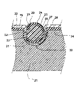
In the Figure 3 a cross-sectional view of spherical bead of
semiconductor is shown 25, 24, 29, 26 placed into the slot 31
the dielectric 21. The flat side of the photodiode bead 32,
such as a Sphelar silicon photodiode (Sphelar Trademark of
Kyosemi Corporation 949-2 Ebisu-cho, Fushimi-ku Kyoto-shi
612-8201 Japan), is aligned to the flat side of the slot 33
or hole. When the bead is aligned correctly it should slip
into the slot 31 or hole 31 and be able to fit almost
completely filling the hole 31. When the spherical bead with
CA 02657099 2009-01-05
WO 2008/005557 PCT/US2007/015623
14
the flat side is miss-aligned with respect to the hole or
slot 31 the bead should not be able to slip all the way into
the hole or slot 31. This key-like feature avoids opposite
polarity of the cells being connected and makes it possible
to use sound to vibrate the beads or vibrate the substrate 21
to "shake" the beads 25, 24, 29, 23, 26 into the proper
orientation and alignment with the semiconductor bead is
placed in the slot the best electrical contacts 23, 26 make
contact with the film contactors 32,27 of the slots or hole
31. By having a film of sticky, electrostatic, or energy
absorbing surface 32 such as silicone rubber at the bottom of
hole or slot 31 the beads will stay in the hole or slot 31
when they correctly have fit the slot and make contact with
the bottom of the slot. The slot can be part of a larger
sheet frame that can be pried open during the filling with
,the beads and when the beads are all in place and can be
tamped in the slots, the larger sheet frame can be released,
thereby creating a clamping force on the beads and making
electrical contact.
In operation light penetrates the semiconductor bead 24, 25
in the P/N junction doped layers 24, 25 region creating
electron-hole pairs (P doped region on the inside 25 and N
doped semiconductor 24 on the outside). The separation of
electron pairs creates the positive polarity of the flat
portion of the bead 33 negative polarity on the outer contact
on the bead 26. The reverse process of supplying a voltage
and current to the P/N junction can be done and the
photodiode can produce light with the recombination of
electron hole pairs_ The P material 25 and the electrical
contact 23 or the electrode 22 can form one junction of a
thermocouple. The N material 24,* electrical contact 26 and
electrode 27 can form the other junction of a thermocouple.
If the semiconductor junction 25, 24 is heated by light or
infrared radiation, the contacts are designed to have
sufficient thermal resistance to allow the semiconductor
junction 2.5, 24 rise in temperature compared to the
CA 02657099 2009-01-05
WO 2008/005557 PCT/US2007/015623
electrodes heat sink 20, 28 and have a temperature gradient
from the semiconductors 25, 24 electrodes contact points 26,
23, and the electrodes 20, 28 then the Seebeck effect will
create a voltage across the cell. These cells can be
connected in series just like the photovoltaic cells and
produce electrical power. If current is passed through these
cells in the reverse direction to the Seebeck effect the
junctions 24,25 will remove heat from the electrodes 20, 28
and heat the semiconductor junction 24, 25 by the Peltier
effect. The electrical contacts 26, and 23 can be formed to
have low thermal conductivity such as forming them point
contacts and dielectric tunneling layers. Other possible
electrical contacts with low thermal transport is to make the
contact 26 partially with a dielectric and have close
proximity electrodes that allow vacuum gap tunneling to occur
moving electrons from the N layer 24 to the electrodes 27.
The elastic compression from the substrate 21 and the sub
layers 19, 34 of the two electrodes 20, 28 on the
semiconductor bead contacts 23, 26 maintains contact
dimensions between these components while the system may go
through a range of temperatures and the coefficients of
expansion may be very different between the electrodes 20,
28, substrate 21, and semiconductors 24, 25. The assembly
of the semiconductor bead in the slot, or hole 31 is then
part of a larger array of cells that are coupled to optics
and electrically connected 28, 20 in series and parallel
circuits for photovoltaic arrays, light emitting diodes,
thermocouples, or Peltier refrigerators or thermionic
converters. In the bottom of the slot 31 a glue 30, be used
to secure the cell into the slot. The glue 30, such as
Sylgard 184, can be optically transparent and act as the
optical coupling material between the substrate material 21
and the semiconductor bead 32, which is desirable in
operation if the sunlight is coming through the substrate 21
into the semiconductor bead 32. The glue 30, can also act as
an anti-reflective coating along with an antireflective
CA 02657099 2009-01-05
WO 2008/005557 PCT/US2007/015623
16
coating 29 on the outside of the bead (anti-reflective
fluorocarbon coatings, Mihama Corporation, 1-2-8 Toranomon,
Minato-ku, Tokyo 105-8437 Japan) It should be mentioned that
rods of the semiconductor 25 could be used in this slot
geometry as well.
In Figure 4 an example of a hole 37 fits the shape of the
bead is shown and the electrical connection 36. The hole has
a flat area with the electrical contact film deposited 35 on
the flat area the dielectric 38 a electrical break area 38 is
masked off and a second electrical contact is shown 39
coating the circular side 40 of the hole 37.
When the asymmetric semiconductor bead shown in cross-
section in Figure 3 is placed in the hole 37 it is allowed to
only slip into the hole if the flat surface 36 of the bead
and the sphere are parallel.
In Figure 5 a cross-section.al view of an array of
semiconductor spheres 52 attached with electrical contacts
54,51,53,55 to the transparent optical lens/mirror 50 is
shown. The photodiode array is formed by coating a shaped
piece of glass 50 that has a curved lens outer area with an
anti-reflective coating on the front surface 58. The back
side of the glass 50 is shaped into concentrating mirrors.
Mirror coatings and an electrical conductive film 51, 53, 55.
are coated on the back surface of the glass 50. The back
side of glass or transparent material EVA 50 has the slots 49
for the semiconductor beads formed in it that is shaped such
that when the shaped semiconductor bead is wedged into the
slot it is elastically holding the bead. A taper of roughly
a five degree slope of the slot wall at the metal to metal
contact point of the bead with the walls will insure that the
bead will be unable to slip out of the slot due to frictional
forces being much higher than the force of sliding out of the
wedge. The mirror coatings and electrodes 54, 51, 53, 55
are deposited with angular controlled vacuum evaporation, ink
jet printing, or angular controlled plasma spraying to coat
the mirror reflector areas and not in the bottom of the slots
CA 02657099 2009-01-05
WO 2008/005557 PCT/US2007/015623
17
49 in the glass 50 to form an electrical break between
electrodes. This uncoated region 49 is transparent to
light. A suitable film for the mirror reflector electrodes
54, 51, 53, 55 is formed by coating the glass with tin which
is then oxidized to tin oxide to be transparent. The
semiconductor spheres 52 are inserted and wedged into the
slot of the glass. A shaped back cover plate is placed over
the array of photo-diodes and glued to the glass optic and
.diode array with silicone rubber sealant. The placement of
the back plate, reflector, and heat sink 56 can apply elastic
pressure on the semi conductor spheres through the dielectric
film 59 of the back plate 56. The dielectric material 59
could be silicone rubber, or polyimide, and may also be the
glue that attaches the back plate to the electrodes 54, 51,
53, 55, semiconducting bead 52 and glass 50. The glue can
also penetrate up into the trough 49 between the
semiconductor 52 and the glass 50 and act as an index of
refraction transition material between the glass and the
semiconductor 49. The sealant is also placed at the perimeter
or the array to seal the semiconductor from dust and dirt.
The aluminum back plate can have a bright polish surface
facing the solar cells, or a white scattering surface. The
exterior surface of the back plate can have a coating such as
black, silicone paint to help the back surface radiate area
keep the back plane cool. Silicone rubber sealant can also be
used to seal the back side of the cells and insure good
thermal contact between the cells and the back plane.
Electrical contact between the electrodes 54, 51, 53, 55 and
the semiconductor beads 52 may be assured by heating the
assembly in a vacuum oven or a flash lamp illumination with
an electric bias to create a large current to weld all the
contacts. Other possible contact securing methods are
ultrasonic pulse of energy to the contacts through glass or
silicon beads to direct heat to the interface contacts.
Soldering leads=to the edges of the circuit 54, 55 may be
attached with ultrasonic pulses.
CA 02657099 2009-01-05
WO 2008/005557 PCT/US2007/015623
18
In Figure 6 an alternative mounting arrangement of placing
the silicon semiconductor beads 65 on the back surface 66.
In this design the back surface 66 is an extruded glass
sheet, polyimide, or a rolled or stamped steel or aluminum
sheet 67, that is coated with a dielectric such as glass 66
and has the silicone bead locating slot 69 formed in it. The
slot 69 has an electrical conducting coating 64 of the silver
or tin vacuum evaporated surface coated on it and a gap 69
that is formed by masking or by the shadow of the shoulder of
the slot 69. An outer surface coating 67 of a reflective
material such as silver, tin or a white scattering material
may be coated the back side of the substrate 66, if the
dielectric is transparent or translucent it will act as a
reflector of light the goes though the insulating gap 69. On
the outer surface 67 a black radiator coating 68 could be put
on. In some cases the black radiator 68 coating and
reflective coating 67 could be omitted and the light that
gets past the cells 65 could be used for lighting the space
under the array.
In this design the light concentrating system is on an
extruded sheet of glass 60. It has an upper lens 61 a lower
array of mirror 62 and slots 63 formed to fit loosely around
the silicon semiconductor photo-diodes 65. To form the
completed array the glass sheet 60 is attached to the
photodiode area with glue such as silicone rubber sealant 85
along the perimeter and possibly between the photodiodes 65
and the glass 60. If the silicone rubber sealant 85 such as
Sylgard 184 is optically transparent it can be placed
throughout the array to act as an optical coupling interface.
The electrical output of this array goes through the
electrical conductive film 64 and out through the edges of
the array.
Figure 7 the arrangement of optical concentration with
three-dimensional optics. In this drawing the lens 70 and
mirrors 71 are packed in a hexagonal pattern 81. Other
possible patterns are squares, and triangles. The optical
CA 02657099 2009-01-05
WO 2008/005557 PCT/US2007/015623
19
concentrator 70 are molded from glass 72. The upper surface
70 forms an array of lenses and the lower surface forms
mirrors 71 and the heat fins.
Total internal reflection of the glass to air interface 70
is used. An electronically conducting film such as tin oxide
is coated 71, 76, onto the surface of the glass on the mirror
areas 77, 80 and into the shaped hole 73, 75.
The two electrodes 77, 80 are separated on either side of
the glass reflector by a gap 79 on the glass reflector 72.
The semiconductor sphere 74, 78 is inserted into the shaped
hole 73 at the end of the glass mirrors making contact with
the two electrodes 71, 76. The insulator gap 79 could be
formed by molding a channel on the side of the glass mirror
72 and then coating the glass reflector with a directional
source of electron conductor material 77, 80 that will not
fill the shadowed area of the gap 79. The insulator gap 79
could be formed by molding a channel on the side of the glass
mirror and then coated into the glass 72 with a directional
source that will not coat the shadowed area of the gap 79.
In operation the light from the sun is focused through the
lens 70 and reflected off the mirrors 71, 76, 75, 77, 79, 80
onto the photodiode cells 74, 78. The higher the
concentrating power of the lenses 70 and mirrors 71, 76 the
increased accuracy the array needs to be pointed at the sun.
With low concentrations, approximately four times, the index
refraction of glass 72 of approximately 1.5 refracts light
from non-perpendicular rays sufficiently such that the
concentrator array effectively concentrates light from the
sun without the need to track the sun. Light that is not
directly focused to the photodiode 74 such as scattered light
through clouds can reflect on the reflective surfaces 71, 76
and partially reach the photodiode 74. The concentrating
photovoltaic array can be fixed mounted tilted to maximize
the output at noon and the latitude angle. Application of
these types of low concentration concentrator photovoltaic
arrays could be used for structural installations and non-
CA 02657099 2009-01-05
WO 2008/005557 PCT/US2007/015623
solar tracking installations. The micro mirrors do not have
to be perpendicular onto the surface plane and in some
designs the mirror could be tilted in the array to maximize
power output and performance when outer surface needs to be
at a defined angle independent of the insolation angles.
In Figure 8 the arrangement of the photovoltaic cell and
micro concentrator when the cells are inserted into a thin
flexible substrate is shown. In this arrangement a substrate
dielectric membrane 90 with slots or holes 108 is formed by
replicating a master surface, curing and then removing from
the master surface. The dielectric replica 90 is then coated
with a directional or surface coating 91, 97,105 to only coat
the outer surfaces and the edges 96,102,104 of the slots or
holes 108. In the case of holes 108 an electric gap can be
provided by a groove slot or impression area 103 of the
substrate 90 other possible techniques are, screen printing,
ink jet printing, plasma spray coating, electroplating, the
metal coatings 91, 96, 97, 102, 104,105 such as silver powder
or tin powder, vacuum deposition of the electrical conductor
film. These electrical conductive coatings 91, 96, 97, 102,
104,105 can have particles in them or cure in such a way that
they form a reliable conductor contact with the semiconductor
photodiode 92, 93, 94, 95 101, 100, 99, 98. A wide variety
of texturing, dimpling, pedestals, fibers, fluting, slitting,
and an elastic polymorphic surface can be molded into the
replica surface contact 96, 102, 104 to help achieve and
elastic electrical contact surface with the contacts on the
particulate photodiode contacts 92, 95, 101, 98. The replica
surface 91, 96, 97, 102, 104, 105 can also contain fibers
and/or have electrical conducting fibers placed in it.
Another method of forming electrical contacts 91, 96, 97,
102, 104, 105 is to laminate electrical conductive foils,
wires, fibers, conductive mesh, conductive fiber matrix, or
powders into the dielectric substrate. The next
construction step is to coat the back side of the molded
dielectric 90 with a back reflector 106 silver, tin, or a
CA 02657099 2009-01-05
WO 2008/005557 PCT/US2007/015623
21
titanium white scattering film. This could be a silicone
paint loaded with titanium dioxide particles. On the
exterior surface of the back reflector 106 a protective and
thermal radiating film 107 such as silicone paint loaded with
carbon black or titanium oxide particles,that radiate in the
infrared and radiantly remove heat from the back side of the
array is deposited. The photodiode spheres 100, 93 with the
doping 99, 94 and electrical conductor contact points 92, 95,
101, 98 are placed in the slots or holes of the structure.
With proper forming of the dielectric substrate 90 and the
electrical contacts 102, 104 photodiode spheres 100 will only
fit elastically in the slots holes 108 one way and achieve
only the proper electrical contacts with the other
photodiodes 93 in the array. With the photodiode array
connected the array could be placed in a vacuum oven to
anneal the contacts 91, 96, 102, 104, 92, 95, 101, 98 and
possibly solder the contacts in place. To protect and
assemble the photodiode array in to a larger module system
they can be embalmed in a material such as chlorofluorocarbon
or coated with silicone rubber sealant and laminated'to a
sheet of glass such as shown in Figure 10 A, 10B, IOC, lOD,
10E, 10F. The cells can be positioned and clamped between a
glass lens and mirror with groves or slots located to hold
the photodiode spheres at the focus or concentration spot of
the lens mirror assembly such as shown in Figure 9.
In Figure 9 a variety of components could be assembled with
the micro concentrator photovoltaic array to form a power
system. Heat removal and thermal storage can be incorporated
with the photovoltaic array management of the waste heat off
the photovoltaic arrays and provide a thermal management of
the photovoltaic array. The micro concentrator photovoltaic
array is shown in cross section in Figure 9 with the
components of anti-reflective coating 117, molded glass lens
110, in interface layer 126, reflector 112, elastic under
layer and dielectric substrate 113, thermal conductive
substrate 114, and radiant coating 125 and back surface of
CA 02657099 2009-01-05
WO 2008/005557 PCT/US2007/015623
22
the photovoltaic array.* The radiant coating 125 could be
textured to have, fibers, fins, bumps, ridges, or dimples to
increase convective heat transfer. The coatings would have a
high infrared emissivity such as titanium dioxide and carbon
black or graphite particles loaded in silicone rubber paint.
It should be mentioned that the molded glass 110 could have a
flat outer surface, which may make it easier to keep clean
from dirt. When the array is assembled between the glass and
the mirror array of cells they are pressed tougher with the
glue in interface layer, such as Sylgard , at or above the
maximum operating temperature of the array and cured at this
temperature. Due to the higher coefficient of expansion of
the glue 126 compared to the mirror array 112, 113, 114, 125,
and glass 110 the glue 126 will shrink and be under tension
at the operating temperatures. This tension in this
interface layer will pull on the mirror 112, dielectric
backing 113, and thermal conductive substrate 114 and
maintain compression on the contacts to the semiconductor
beads 115. The electrical current is collected from the
series connection contacts 112 on the 115 beads and delivered
to the side of the array. The electrical output from the
photovoltaic array is shown schematically as positive 116 and
negative terminals 111. An enclosure 120 can be placed on
the back of the photodiode array 125. This enclosure 120
could be a simple as a chimney to direct convective air flow
past the photovoltaic arrays 125 or could be a circulated
fluid 122 such as fluorocarbon, alcohol, or water. A typical
arrangement that minimizes the corrosion impact on the
photovoltaic array 125 is to have air 122 pumped with a fan
121, 123 past the photovoltaic array 125, and the heated air
122 is used for structural heating. The fan or pump 121, 123
can be run when it is necessary to cool the photovoltaic
arrays 125 or deliver heat to the structure. The ridge or
bumpy exterior 125 of the photovoltaic array achieves a
better heater transfer coupling from the photovoltaic array
into the flowed fluid 122 than a planar photovoltaic array.
CA 02657099 2009-01-05
WO 2008/005557 PCT/US2007/015623
23
A phase change material 119 can be placed on the back of the
array 125 or in the flow plenum 120 to temperature stabilize
absorb heat and thermally store heat in the system. The DC
electrical output 116, 111 can be connected to an electrical
conversion system 118 that optimizes the performance of the
photovoltaic array and converts the electrical output to a
desirable electrical output such as 110 Volt alternating
current. Capacitors, reversible fuel cells, and/or batteries
could be incorporated in to the electronics conversion system
118 to store electrical energy adjacent the array 125. A
heat pipe system 120,124 could be incorporated in the back of
the photovoltaic array 125 to delivery waste heat efficiently
to structures. The heat pipe 120, 124 could have a boiling
point set by an impurity with the working fluid 124 or
elastic walls 120 to create a constant pressurization of the
heat pipe to set the boiling point of the heat pipe to only
remove heat when the array temperatures are useful to be
delivered to the structure.
Various coatings 117 such as infrared and UV absorbing film
of titanium diode films, such as TPX solTM titanium dioxide
coating, Kon Corporation, 91-115 Miyano Yamauchi-cho,
Kishima-gun Saga prefecture, Japan, may be applied to the
outer surface of the glass to reduce the heat flux on the
photocell from the un-utilized infrared solar radiation,
bellow the band gap of the semi-conductor. The
antireflective coating 117 could be a material such as
titanium dioxide that absorbs IN light and photo
catalytically oxidizes organic material on the outer surface
of the glass to keep the surface transparent and reducing
possible UV damage to the glass 110 and photovoltaic array
1115, 112, 113, 114, 125.
Figures 10A, IOB, lOC, 10D, 10E, 1OF and 10G show various
alternatives light concentrating systems that can be coupled
to the elastic contacted cells.
In Figure 10A a lens array 130 with precision placement of
photodiodes 132 in elastic contacts 133 is shown. An air gap
CA 02657099 2009-01-05
WO 2008/005557 PCT/US2007/015623
24
109 between the lens arrays provides for thermal insulation
where this array may be used as a glass window or skylight.
The electrical contact film can be a transparent tin oxide.
Contact breaks 134 are shown between the cells, and elastic
dielectric such as silicone rubber layer 128 and a
transparent dielectric substrate 127, such as a flat molded
glass sheet, are shown. In this arrangement, light 131 would
pass through the lens array 130 to focus onto the
semiconductors 132 without reflecting off mirror electrodes
133. This system does not capture light that does not reach
the focus at the photodiode 132. Thus, diffuse light with
low angles 129 to the surface other lens surface 130 would
reflect or pass through the arrays if the electrical contacts
133 are reflective or transparent. The light transmission
optical arrangement could be useful for room lighting such as
a skylight or windows where the direct sunlight is captured
while light that has a low angle to the surface 129, such as
morning and evening light, scattered light off the clouds and
scattered light of the atmosphere misses the photodiode 132
and passes into the room. In this example the semiconductor
contacts 133 are shown on a flat substrate 127, but it could
be a shaped substrate 127 that helps hold the semiconductors
and uses light reflections off the shaped electrodes 133 on
the elastic layer 128 and the substrate 127 to collect light
to the semiconductor 132. A possible additional feature is
to have the elastic layer component 128 be a phosphor or
scintillator and convert light that is absorbed in this layer
converted to a characteristic emission light of the phosphor
or scintillator. Examples of scintillator materials are
anthacene that can be dissolved and dispersed into polymers
or rubber (Pfaltz and Bauer, 172 E. Aurora St. Waterbury CT
06708). An example of a phosphor is zinc sulfide (ZnS)
activated with dopants of copper or silver. Another example
of a phosphor is yttrium aluminum garnet crystals that
convert blue light to yellow light. The characteristic
emission light is emitted at all angles but due to total
CA 02657099 2009-01-05
WO 2008/005557 PCT/US2007/015623
internal reflection of the elastic sheet of material 128 and
the reflections off the electrodes 127 and the a substrate
material 127 internal reflections the light is conveyed to
the photodiode where the elastic layer 128 changes angle and
thickness. An advantage of using a scintillator compared to
the phosphors is that is does not absorb it's own
characteristic light and lower energy photons, thus it can be
used in the transmission components 130, 109 and the elastic
layer 128 letting the lower energy photons focus through the
optics. The scintillating layer due to internal reflections
and low characteristic light absorption can effectively
collect converted light from a large area or volume of
optical components 130, 109, 128 and deliver it to the
photodiodes 132. Phosphors and scatterers would be expected
to be used on non-tranmissive components such as the
electrodes 133, elastic layer 228, or substrate 127 and could
also be used to redirect non-focused light 129 to the
photodiodes 132.
In Figure 10B a Fresnel or holographic light concentrator
137 is shown as the light concentrating element. This is an
example of different types of optics,could be used to
concentrate light to the discrete photodiodes. In this
example a cross sectional view of a Fresnel lens 137 is
shown. Light 136 passes through the transparent lens
material 137 and then is refracted from the facets of the
Fresnel lens and is focused to the semi conductor 138. The
optical element 137 could also be a holographic lens that can
concentrate light to the photodiodes 138 by a diffraction
pattern such as grooves in the interior surface of the
transparent material 137 instead of refraction with a wide
range of incident angles to the photodiode 138. In this
example the substrate material 139 is a shaped elastic
polyimide substrate for the contact electrodes 126, 140
holding- the silicon photodiode 138. As in the previous
example in Figure 10A the elastic substrate 139 could be a
scattering surface, scintillator, or phosphor and act like a
CA 02657099 2009-01-05
WO 2008/005557 PCT/US2007/015623
26
converter and conduit of light that is not initially focused
to the photodiode 138.
In Figure 10C an example of -a back reflector and photodiode
array on front=surface is shown. In this example the
incident light passes 143 through the elastic substrate and
the electrical conductors. The light 143 reflects off the
aluminum reflector 145 and is concentrated onto the
photodiode 142. The photodiode 142 is held with two
transparent electrical contacts 144, 164 such as tin oxide or
thin network of opaque silver electrical conductors that are
held onto the photodiode with elastic substrate material such
as fluorocarbon. A transparent material 162, such as
silicone rubber, could be placed between the conductive
.electrodes 144 and the mirrors 145. The transparent elastic
substrate material 141 such as fluorocarbon plastic is shaped
to form an elastic clamp around the semiconductor body 142
and also act as a lens for the direct incident light.
In Figure. 10D a Cassigranian light concentrating system
with photodiode 150 on the back surface is shown. In this
arrangement the light passes through a transparent glass
cover sheet 146, through air or transparent material cavity
153, reflects off a shaped mirror 147, makes a second
reflection off a shaped mirror mounted 147 on the glass cover
sheet, and is focused to the photodiode 150. The
cassigranian optics have a light collecting disadvantage that
the second reflector blocks direct rays from reaching the
semiconductor, but this could be useful if there is a need to
shield the photodiode 150 from high energy radiation. The
second mirror 147 could incorporate shielding material.
Electrical connections are made to the photodiode 150 through
the shaped aluminum mirrors contacts 149 on the silicone
rubber elastic sub layer 151 and assembled on the polyimide
dielectric substrate 152. The elastic sub layer 151
maintains contact pressure on the photodiode 150 even though
the entire system experiences differential expansion between
the components 152, 151, 149. An optically transparent
CA 02657099 2009-01-05
WO 2008/005557 PCT/US2007/015623
27
material such as silicone rubber could be placed between the
front surface 146 and the reflectors 149.
In Figure 10E light concentrating optics using a gradient
index of refraction lens is shown. In this arrangement the
optical material is the elastic substrate, such as doped
silicone rubbers and fluorocarbon polymers, are layered and
shaped in increasing index of refraction layers 155, 156,
157, 161 to focus the light to the photodiode 160. Light
rays refract 158 off the shaped layers of the silicone
rubbers 155, 156, 157, 161 to focus on the photodiode 160.
The contact electrodes 159 are elastically pressed onto the
photodiodes. The last layer of the refractive material is
molded to form compression cavity 161 when the photodiode is
pressed into the cavity. The cavity 161 is designed with the
electrodes to make junction contacts onto the photodiode 160.
In Figure lOF a tilted or off-axis concentration scheme is'
shown. This allows the array to not be perpendicular to the
rays 165 from the sun for possible architectural reasons or
this tilted to incident light 165 surface geometry to take
advantage of chromatic aberration. The index of refraction
spread to the light spectrum can be used with the tilted
refractory surface to place different wavelength portions of
the light spectrum into different photodiodes that are
optimized for that portion of the solar spectrum. Typically
light passing at an angle through a refractory material
resulting in red light 171 refracting with the largest
angle and then green light 172 and finally blue light 169
with the lowest light refraction. Thus a row of photodiodes
170,168, 169 can be arranged to optimally intercept the =
spectral spread of light: red light photodiodes 170 in the
first row, green light photodiodes 168 in the second row and
blue light outer 3,d row of photodiodes 169 in reflective
slots 167 coupled with micro concentrator glass 166 with a
tilted geometry. The photodiodes are placed and glued into
the shaped elastic cavities in the elastic transparent
CA 02657099 2009-01-05
WO 2008/005557 PCT/US2007/015623
28
refractory material with a silicone rubber such as shown in
Figure 3; with electrical contact film making compression
contact 167 to the two sides of the cells stacks 170, 168,
and 169.
In Figure 11 a multilayered photodiodes semi-sphere with
layers of different band gaps 181, 184, 180 are shown in
cross-section. A partial cutout of a spectral spreading and
focusing lens 176 is also shown. The blue photon absorbing
high energy band gap photodiode layer 180 is the outer layer
of the semi-spherical photodiode. A green light absorbing
and intermediate band gap energy photodiode layer 184 is the
next layer of the semi-sphere. A red light absorbing and
lowest band gap layer photodiode 181 is the core semi-sphere.
Three layers of semiconductors 181, 184, 180 and separating
electrodes are shown as an example of possible layered photo
diodes in a semi-spherical geometry. More or less photodiode
layers could be used and can be formed by multiple coatings
of the central sphere 181. Each photodiode layer 181,184,
180 will have impurity doping or inter-electrode layers that
create a concentration=and voltage gradient of a photovoltaic
photodiode. On the outside of the photodiodes an anti-
reflective coating 174 outer layer of the semi-sphere is
added. This anti-reflective coating 174 could be a gradient
index fraction material or could be a quarter wavelengths
thick transparent material coating that achieves anti-
reflection by destructively interfering with the reflection
of light. To optimize the light transmission to the
photodiodes 181,184,180 the anti-reflective coating 174 could
be adjusted to maximize the red light 178 transmission at the
top of the photodiode semi-sphere and then optimize the
transmission for the shorter wavelength 177, 199 of light on
the sides of the sphere. Due to the spherical shape and the
angle of incidence of the light on the sides of the sphere a
uniform thickness quarter wavelength anti-reflective coating
174 will shift the peak transmission to longer wavelengths.
Thus, for light concentration systems and when the light
CA 02657099 2009-01-05
WO 2008/005557 PCT/US2007/015623
29
direction is controlled onto the photodiode spheres in
general the=optimum quarter wavelength anti-reflective
coating 174 would be thinned on the sides of the sphere to
compensate for the angle of incidence change. For this
particular example when the light is spectrally distributed
onto the photodiode sphere the quarter wavelength
antireflective coating 174 can be thinned even more on the
sides of the sphere to optimize the light transmission for
the green and blue light 177 incident on the sides. A
thickness profile varied coating of this type could be
accomplished with a vacuum evaporated source and using the
effect of angle of incidence on semi-sphere producing thinner
coatings.
The layered photodiode semi-sphere 181, 184, 180, 174 is
placed behind the focusing optics 176 near the focal.point
for red light 179. Incident white light 175 is spectrally
spread with chromatic aberration where the index of
refraction varies with the wavelength of the light.
Typically red light 178 through glass has a higher index of
refraction than green 199 and blue 177. The semi-sphere
photodiodes 181, 184, 180 are placed after the focus point
179 of the red light of the lens 176 such that it optimizes
the spatial distribution of colored light spectrum into the
layered photo diodes to place the red light focus 179 just
outside the photodiodes or inside the central red light
absorbing photodiode 181. In turn the green light 199 will
form a larger spot and is absorbed more efficiently into the
green light absorption band of the photodiode due to the
longer path length through the tilted photodiode layer 184.
The blue light 177 spot will be the largest diameter and most
efficiently absorbed in the outer photodiode layer optimized
for blue light absorption and conversion. The longer
wavelength red light 178 in general will refract through
glass 176 at a higher angle than the green 199 and blue light
177. The red light 178 will pass through the blue 180 and
green light photodiodes 184 with low absorption due to being
CA 02657099 2009-01-05
WO 2008/005557 PCT/US2007/015623
below the excitation band gap of these two photodiodes.
This spectral, spatial, and angular distribution of light on
to the layered semi-spherical photodiode 181, 184, 180 will
tend to optimize the performance of each of the photodiode
cells without having to have physically separate the
photodiode cells. Some of the green 199 and red 178 light
will strike the blue 180 and green 184 optimized photodiodes
with these light photons below the band gap energy of the
blue and green light optimized photodiodes and partially
passes through and onto the green 184 and red 181 layered
photodiodes. This layered construction of a layered
spherical photodiodes could be less expensive than forming
distinct photocells that are then placed together. The
electrode contacts in this geometry are shown as attached
conductive metal contacts 183, 181. The inner layer contact
182 is attached to the exposed surface of the center of the
red photodiode 181, and the outer contact 183 is attached to
the surface of the outer blue photodiode layer 180 and
through the anti-reflective coating 174. Examples of
details of elastic contact geometries to this semi-spherical
bead are shown in Figure 3, Figure 12B and Figure 14.
Ideally the electrical contacts 182, 183 reflect light and do
not block light to the photodiode such as in the elastic
contact example of Figure 14 for this circular spot focus.
A mechanical contact would need to make central contact with
the central spot contact 182 and use the alignment of the
silicon sphere with the form fitting surface to allow only
proper electrical contact and placement of the layered
photodiode into the radial spectral dispersion pattern of red
light in the center and blue light on the perimeter.
It should be mentioned that a roughened or density gradient
antireflective coating 174 may be advantageously used in this
geometry to avoid spectral and angular selectivity of the
typical quarter wavelength anti reflective coating and
mentioned earlier.
CA 02657099 2009-01-05
WO 2008/005557 PCT/US2007/015623
31
If a slot version of the semiconductor holding cavity is
used the central contact could have a raised button 182 and a
dielectric perimeter 185 coating such as the anti-reflective
coating extended to cover the edges of the green 184 and blue
180 photodiodes to prevent shorting to the electrical
contacts along the groove.
In Figure 12A an alternative arrangement of forming
photodiodes by grinding the particulate bead layered
photodiodes on two sides. By grinding the beads on two sides
the inner doped layer 274 and other photodiodes 272 can be
accessible with two electrical contacts 273, 275. This
geometry of a bead with two flat sides versus a single flat
side can also be advantageously used to make electrical
contacts_ As an example of a layered photodiode an InP bead
five hundred microns in diameter is formed 274. The InP bead
274 is doped to be an n-type semiconductor. The InP bead is
then coated with an n-type InGaAs layer 272 by organometallic
vapor phase epitaxy approximately two microns thick. Then a
p-type InGaAs layer 271 two microns thick and a sputter
deposited gold chromium coating 270. The bead is then ground
on two sides and the electrical contact is formed deposited
by vacuum deposition or electroplating a nickel/gold contact
272, 275 to the center. There are many variations of
materials to produce layered photodiodes or photo emitters.
Other suitable substrate bead semiconductors are Ge, Si, SiC,
GaAs, GaP, Ga, GaN, CdTe, AlGaP, AlGaP, AlGaAs, CuInSeZ,
Cu (InGa) Se2, GaSb, InAs, CuInSe2, Cu (InGa) Se2, CuInS, GaAs,
InGaP, AlGaP and CdTe.
In Figure 12B slot or cavity electrical contact to
photodiode bead with rim 281, 292 and center contacts 286,
287 are shown. In this example the photodiode bead as
constructed by grinding a layered photodiode bead on two
sides, as shown in Figure 12A, is inserted into the elastic
slot 295 in a dielectric 288 with two side contacts 280, 287
and a backing contact 289. The slot or cavity 295 is molded
out of an elastic dielectric 288 such as polyimide or
CA 02657099 2009-01-05
WO 2008/005557 PCT/US2007/015623
32
silicone rubber on top of a metal foil substrate 289 such as
tin. The photodiode bead.281, 282, 283, 284, 290, 291, 292
is pressed into the slot 295. The two side contacts 280, 287
compress against the to center contacts 286, 285 of the
photodiode bead. The rim conductor 281, 292 of the
photodiode bead makes contact with the foil contact 289 at
the bottom of the slot or cavity 295 with elastic compression
from the cover lens 293 or mirror pressing the photodiode
bead against the back contact. The molded cover glass 293 is
held by tension and sealed to the contact electrodes 280, 287
through a Sylgard transparent interface glue 294 that is
cured at elevated temperature under compression pressure
between the glass 293 and the electrode substrates 288, 289.
At the lower operating temperatures than the glue cure the
thermal contraction of the interface glue 294 creates a
tension in the glue pulling the cover glass and the
electrodes word each other and creating contact compression
pressure. Other mechanical elastic, gravity or force schemes
can be used to maintain the elastic contact pressure on the
photodiode 281, 282, 283, 284, 290, 291, 292.
In Figure 13A a semiconductor bead alignment and
manipulation system is shown. In this system the
semiconductor beads 188 that have a flat side 189 are
vibrated by sound 186 from a sound generator 185 or
vibrations through the support plate 190. The beads 188 will
spin until they reach the lowest energy on the flat side of
the beads resting on the flat Teflon 187 surface with gravity
holding them down. Different intensities of sound vibrations
186 can be used to manipulate the beads to move them far off
the surfaces or to have them gently rotate and settle to the
lowest energy state flat side of the bead 189 on the Teflon
surface 187. The Teflon 187 has an electrostatic charge thus
attracting the beads 188 and increases the energy well for
the beads to stay on the flat side 189 resting on the flat
Teflon surface 187. A high voltage electrode 190 can be
placed behind the Teflon 187 surface and high voltage applied
CA 02657099 2009-01-05
WO 2008/005557 PCT/US2007/015623
33
from a generator 191 to the electrode 190. A sharp point
corona discharge to the semiconductor beads 188 or adjacent
electrode 193 or surrounding grounded 192 conductive surfaces
can complete the electrical charging circuit and electric
field lines to the charge electrode 190. The induced
electric field and the charge on the semiconductor beads 188
hold them against the Teflon surface 187.
Shown in Fig. 13B due to the low coefficient of sliding
friction of the Teflon surface 204 the beads 201, with their
flat sides aligned to the surface, can slide across the
Teflon surface 204 without rolling with a pushing bar 200.
The pushing bar 200 can push the semiconductors 201 to align
the semiconductors in rows with all the flat sides against
the Teflon surface 204 on a support plate 205. The pusher
bar can have shaped cavities 202, 203 to hold individual
semiconductors in discrete positions. If a semiconductor
has the wrong position or there are too many semiconductors
to from a single row these beads will not fit into the shaped
cavity 203 of the pusher bar 200 and can be separated from
the beads 201 that have fitted into the slots 202 or holes
203 of the pusher bar and ejected, contact lifted with a
silicone rubber surface, or swept off the Teflon surface 204
and the pusher bar 200.
Shown in Fig 13C a cross-sectional view of the pusher bar
216 being used to press the semiconductor beads 213 into the
shaped mirrors or electrical contacts and elastic substrate
210. The electrical charge on the support plate 218 can be
released or reversed as the beads 213 are slipped into the
shaped cavity 212 electrical contacts 211, 219. The pusher
bar 216 can also be heated and/or can have sound pulsed
through it to solder or weld the beads 213 contacts 214, 220
to the electrical contacts 211, 219 once they are inserted
and clamped by the electrical contact holder 210. The beads
can be heated by light or magnetic fields once they are
inserted into the holders to achieve soldering or welding of
contacts 214, 220. The semiconductor beads could have
CA 02657099 2009-01-05
WO 2008/005557 PCT/US2007/015623
34
electrical contacts 214, 220 that are made of magnetic
material such as nickel. Thus the magnetic attraction to a
magnetized surface 218 or alignment in a magnetic field could
be used to align and hold the beads on a holder 218, 217.
Other properties that may be utilized to align the beads is
to use the self polarized electric field of the beads 213 in
an electric field to align the beads 213. It should be
mentioned that sticky and electrostatic properties of
silicone rubber coated surfaces 215 can act as bead holders
allow beads to held without rolling and transferred. The
insertion of the semiconductor beads can done with the shaped
aperture 212 electrical contacts 211, 219 on the elastic
backing 210 being held open for the insertion and then
released to mechanically clamp down on the beads 213 and make
electrical contact of the round bead contact 214 to the
rounded electrical contact 211 and the inner bead contact 220
making contact with the flat surface contact 219 of the
elastic holder 210. The mechanical clamping of the holder
210 also allows the beads 213 to be held to allow the pusher
216 to separate from the beads 213 and retract the pusher
216. The pusher 216 could have a silicone sticky surface 215
inside the formed surfaces 222 to allow aligned beads to
stick in the cavities and non-aligned beads to be shaken off.
In Figure 14, the lens mirror electrode compression
arrangement is shown in cross-section. Another arrangement
of connecting the spherical ground semiconductor photodiode
or ground rod 233 is to form a cavity with the mirror
contacts 237, 238, 242 that will only permit the cell to be
connected in one orientation. The shaped depression, or
troughs 239, 241 have a center contact 242 and side contacts
239, 238 as shown in Figure 14. These contacts 237, 238, 242
and vias 243 can be formed by ink jet spraying electrically
conductive powder inks such as silver, copper, nickel,
graphite, aluminum, tin, and alloys onto the dielectric
substrate such as molded or shaped polymimide 239, 241.
Other methods of forming the electrical contacts and circuit
CA 02657099 2009-01-05
WO 2008/005557 PCT/US2007/015623
films 237, 242, 238, 243 are sputter deposit, plasma sprays,
electroplating, foil embossing, electrically conductive films
onto the pre-formed flat sheet or formed dielectric substrate
239, 241. Other options are to coat or laminate a sheet
metal substrate to hold the form of the contacts and act as
another back protective surface 244. The side contacts 237,
238 have a dielectric coating 235, 236 deposited part way up
from the flat bottom of the electrical contact 237,238 and
dielectric backing substrate 239, 241 to not allow the semi-
spherical bead 233 to make electrical contact with the side
contact electrodes 237, 238 if the rounded surface of the
bead 233 is touching the center electrical contact. The
dielectric coating 235, 236, such as Teflon or silicone
=fluoro polymer, can have a low coefficient of friction to
permit the semispherical bead 233 to easily slip and spin
until the flat side of the semiconductor photodiode bead 233
orients parallel flat surface bottom of the trough or
depression 239, 241. With gravity holding the loose bead
down toward the bottom of the trough or depression 239, 241
and with the bead fitting the deepest into the trough or
depression with the flat side of the bead 233 parallel to the
bottom they will reach the lowest energy state. If vibration
energy or sound energy is imposed upon the semi-spherical
beads, the beads can rotate and spin until the flat section
of the beads fits against the flat bottom of the trough or
depression 239, 241. This gravitational effect can be
enhanced if electric fields are imposed between the
electrodes 239, 242, 238 and an exterior electrode not shown.
The dielectric films 239, 241, 234, 236 often are permanent
electrets or can be poled and charged with imposed electric
fields. By forming the center contact 240 on the semi-
spherical bead 233 with a ferromagnetic material such as
nickel and making the center contact 242 out of a
ferromagnetic material such as iron or nickel and then having
the contacts 242, 240 be magnetized or placed in a magnetic
field the bead will preferentially be oriented in the
CA 02657099 2009-01-05
WO 2008/005557 PCT/US2007/015623
36
magnetic field and the magnetic fields will be channeled and
concentrated through the cent'er contacts 240, 242. This
would increase the energy well of the aligned beads with the
flat surface of the bead 233 parallel to the trough or
depression 239,241 of the mirror contacts 238,237. The side
electrode surfaces 237, 238, make contact with the sides of
the semi-spherical bead 233 when the beads are correctly
aligned. The photodiodes semiconductor bead 233 will
typically be doped to have a positive charge carrier doping
on the interior and a negative charge carrier doping on the
outside. Thus electrical contact on the flat surface of the
bead 240 is making contact 242 with the P interior layer and
the outer surface contacts 237, 238 are making contact with
the N layer. Due to the differences in coefficient of
friction between the side contacts 237, 238 of the bead 233
with the dielectric coating 235, 236 and the side contacts
237, 238 the beads 233 will tend to stick into the depression
239, 241 once they make metal contact. The shape and
elasticity of the trough or depression 239, 241 can be made
such that it forms a wedging contact 237, 238 on either side
of the bead to hold the bead once it makes correct alignment.
It may also be useful to have the alignment process occur at
an elevated temperature near where the bead side contacts
237, 238 will solder or sick to the bead 233 outer surface,
thus also making the side contacts sticky to the beads and
holding the beads once they have made parallel surface
alignment and electrical contact. Other possible holding
schemes are to have small droplets of glue, silicone rubber,
or viscous liquid on the dielectric separator 239, 241 in the
bottom of the trough or depression that when the bead flat
surface is aligned reduces surface tension energy by making
contact with the flat surface of the bead 233. This will act
as a bead holder and increase the energy well to hold the
beads in the flat surface of the beads parallel to the flat
surface of the trough or depression. To remove excess or
non-aligned beads 233 the assembly could be flipped over and
CA 02657099 2009-01-05
WO 2008/005557 PCT/US2007/015623
37
let gravity pull out beads 233 not held in place. Other
options are to place a formed tool with a sticky surface
coating, such as silicone rubber, such that when it is
lowered over the surface of the array it will make mechanical
contact with only the excess beads. The beads 233 in the
incorrect positions will rest higher in the troughs or
depressions than the parallel surface aligned beads 233. A
process of checking that all beads 233 are aligned could be
done by visual inspection or having a precision tool with a
vacuum or sticky surface that fits into the trough or
depression and only makes contact and remove cells that are
not fitting correctly into the troughs or depressions 239,
241. Once the flat surface of the bead 233 is aligned to the
flat surface of the trough or depression 239, 241, 237, 238
the electrical contacts 239, 240, 242, 238 can be assured by
heating the semiconductor bead 233 with a flash of light, or
thermo mechanical contact to the beads 233 with heated metal
body touching and compressing the beads 233 against the
electrical contacts 237, 242, 241. Other possible methods
of delivering energy to make solder, brazing, or welding
contacts are to pulse ultrasonic sound energy into the
semiconductor beads 233 and contacts 237, 242, 238 to
friction weld or solder the contacts. An electrical pulse
through the circuit and cells 237, 238, 233, 240, 242 can
also be used to create arc welding of the electrical contacts
to the semiconductor photodiode beads 233. Another
electrical contact welding, brazing, annealing, or solder
method is to use self generated electrical pulse from the
semiconductor photodiode 233 if the electrical circuit 237,
238, 233, 240, 242, is short circuited, attached to an
electrical source, or charged capacitor and then a beam of
laser light is rastered across the cells or a flash lamp is
fired next to the cells. Creating a short electrical pulse
to provide a short thermal energy pulse at the mechanical
contact points to the welding, brazing, annealing or
soldering the contacts. The center contact 242 or side
CA 02657099 2009-01-05
WO 2008/005557 PCT/US2007/015623
38
contact metal films on top of the dielectric substrate 241
can be designed such that they act as an electric fuse
melting and vaporizing the metal 242, 237, 238, 243 and
expanding the underling dielectric 239, 241 to open the
circuit if the local circuit if excessive current flows
through the circuit. This could be used to disconnect cells
that may have been miss-connected or are shorted. The
contact assurance step can also be done after the assembly
under the refractory lens and mirror 231 is placed over the
cells and they are held in place by the refractory lens and
mirror 231. The refractory cover leris and mirror 231 can
press against the semiconductor bead 233 to make electrical
contacts and maintain electrical contact throughout the
lifetime of the solar array. The refractory cover 231 can be
pressed and held with glues 232 and elastic tension in the
electrical contact material 237, 239, 238, 241, 242 and
gravity of the refractory material resting on the
semiconductor 233 against the contact material 237, 242, 238
can maintain contact over the life of the array. The
lens-mirror assembly sheet 231 can have a protective or
antireflective coating 230 on the outer surface. Suitable
films are fluorcarbons (Mihama) , titanium dioxide coatings
to make the outer surface photo reactive and self cleaning or
hard anti- scratch coatings such as reactive sputtered
diamond films. Optically transparent glue or coupling gel
234, 232 (such as Dow Corning Sylgard 184 or gel Q3-6575)
is dispersed such as with a high pressure extrusion over the
cells. The glass or transparent dielectric cover lens-mirror
231 is places over optical coupling material 234, 232 and
with a roll squeezing motion optical coupling material 234,
232 is pressed around the semiconductor and mirrors the gas
bubbles are pressed out of the assembly through gas channels
in the pattern of the glue. The entire assembly can be
cured with elevated temperatures. The assembly can be cured
under compression to press the lens-mirror sheet 231 against
the semiconductor beads 233 and maintain compression on the
CA 02657099 2009-01-05
WO 2008/005557 PCT/US2007/015623
39
electrical contacts 237, 240, 242, 238. Shrinkage of the
glue or optical coupling material 234, 232 after or during
the curing process could further increase the compression of
the lens-mirror sheet 231 onto the beads 233 and contacts
237, 240, 242, 238 during and after the curing process. On
the backside of the dielectric substrate 239, and the metal
contacts 242 a radiant heat transfer and protective coating
244 such as carbon black loaded silicone paint or titanium
dioxide silicone paint. The assembled system can be tested
and with light pulses, rastered laser beams, or electrical
pulses shorted cells or reversed'cells can be removed from
the array parallel series electrical circuit by melting or
vaporizing electrical contacts. Electrical connections to
the outside electrical systems and circuits are expected to
be made through electrical contact pads at the edges of the
glass material sheet 231.
Figure 15 an electrical circuit of series parallel cells
with thin film electrical conductors or dielectrics, fuse, or
varistors 253, 258 in the parallel and series connections
between photovoltaic cells 253 and back flow protection
diodes 254 or varistors 254 built in on the output is shown.
The reverse flow protection component 254 can also be placed
by the same method of doped semiconductor beads placed in
elastic shaped electrical contacts with the reverse electron,
hole gradient to the photodiodes as indicated in the
schematic drawing Fig. 15. The reverse current protection
diodes 254 are not illuminated and therefore can be placed
outside of the light concentration regions either between the
mirror arrays on the edges of the arrays. The reverse
current protection diodes 254 can be placed periodically as
rows in the array to be able to match the protection diodes
voltage and current characteristics and create distributed
reverse current protection avoiding any single protection
diode or string of protection diode failures jeopardizing the
entire system. The fractional loss effect of a single cell
becoming an open circuit in parallel connected cells is one
CA 02657099 2009-01-05
WO 2008/005557 PCT/US2007/015623
divided by the number of cells connected together. The-effect
of a single point failure on the entire system from a single
.point failure in a series parallel electrically connected
.network is proportional to the fraction of loss in a row
divided by the number of rows since the current from the
other rows will be able to flow around the single point
failure. The number of random single cell failures is
proportional to the total number of cells in the circuit.
Therefore in large arrays of many parallel connected cells at
equipotentials and series connections where the number of
cells in any single row is proportional to the square root of
the total number of cells in the array the probable
fractional loss from random single open circuit failures is
proportional to the inverse square root of the total number
of cells in the array. This statistical observation has the
practical implication that with series parallel arrays; the
higher the number of individual cells in an array the lower
the lower the fractional losses due to random cell failures.
These photovoltaic arrays become more reliable the higher the
number of cells, which is contrary to typical intuition that
the more cells in an electric circuit the more probability of
failures and output loss. In high.voltage arrays the
reverse current protection cells 254 and bypass diodes 257
can be periodically formed in rows in the arrays. The
parallel electrical connections 253 between cells are useful
in having a current bypass around single cells in the array
that may have low performances due to manufacturing defects
or shading. The bypass diodes 257 can route current around a
row of cells 252 that have a low performance or be shadowed.
The parallel 253 and series 258 electrical connections can
form effective fuses by thin conductive deposits on
dielectric insulator substrates or varistors by depositing
with the electrical conductors semiconductors that have been
chosen to have a specific electrical resistively increase as
the current, voltage or temperature rises. A particular
example a film of zinc oxide will increase its resistance
CA 02657099 2009-01-05
WO 2008/005557 PCT/US2007/015623
41
with applied voltage. The deposits can be vacuum sputter
deposits, spray ink deposits, plasma spray deposits, foil
embossed, individual semiconductor deposits similar to the
photodiode bead connections. Most metals have the desirable
characteristics of a low resistance at ambient temperatures
and then increasing resistance as the temperature rises. If
excessive current flows through the parallel or series
electrical connections such as several times that of single
diode, the metals heat due to ohmic energy dissipation in the
material. If the current and heat generated is high enough,
the circuit would melt the metal and possibly the dielectric
substrate and permanently open the parallel circuit
connection. Open circuit fusing between the cells 253 can be
used to permanently open the circuit around individual photo
cells 252 if they are shunted or connected in reverse.
Devices such as varistors 253 can be formed in the parallel
circuit connections that are designed to have and increasing
resistance as current rises. The varistors 253 could be
designed to reversibly respond rapidly to excessive current
and effectively clamp the maximum current in the parallel or
series connections. This maximum current clamping can be
very important to protect the photodiodes from excessive
currents and voltages in situations where an illuminated
photovoltaic array is selectively shadowed such as a shadow
from a tree limb. This array schematically shown can be
connected 250, 256 through the perimeter bus connections 251,
255 to other arrays or the electrical loads. Other possible
electrical devices that could also be electrically connected
on the output connection or bus connection 250, 256 and
integrated with the array as shown in Figure 9 are DC to DC
converters, DC-AC converters, capacitors, batteries,
electrolysis cells, flywheels, motors, lights, pumps, and
fans.
Some features and elements of the invention include:
1. The electrical contacts maintain compression on the
semiconductor bodies with elastic mechanical systems.
CA 02657099 2009-01-05
WO 2008/005557 PCT/US2007/015623
42
2. Use.the shape of the photodiode body or electrodes to
orient the semiconductor.
3. Use a slot or hole to fit the cell.
4. Use the flat side of the sphere to hold, orient and move
to the electrical connection.
5. The slot is also an electrical connection.
6. The slot is also a mirror.
7. The slot is also light transmitting.
8. The position and dimensions of the electrical contacts
on the spheres can be advantageous for semiconductor
operation.
9. The electrical contacts have thickness to provide for
electrical properties of fuse and circuit interruption.
10. The electrical contacts can be mirrors.
11. The electrical contacts can be transparent.
12. The electrical contacts can be dissimilar electrical
conductors or metals.
13. The electrical contacts and semiconductor can
essentially form a thermoelectric junction.
14. The electrical contacts and semiconductor can form a
light producing junction.
15. The slot and electrical contacts form a heat removal
system.
16. The electrical contacts and or mirrors are heat
conductors to remove heat from the photodiodes.
17. A coating on the back side of array enhances the radiant
emission and heat removal.
18. The mirror/lens is a heat removal system.
19. The mirror/lens is a mechanical mount and protection
system.
20. Use parallel series connections to provide reliable
circuit connections.
21. Can use glues.
22. Can use optical interface bridges or glues.
23. Can use light curing glues.
24. Can use sticky materials to secure cells in slots.
CA 02657099 2009-01-05
WO 2008/005557 PCT/US2007/015623
43
25. Can compress spheres in slots to make contacts.
26. Can use soldering to complete contacts.
27. Can use welding to achieve electrical contact securing.
28. Can use a flash lamp to achieve electrical contact
securing with the photo diodes generating the electrical
current to weld and or thermal heating of the cells.
29. Can use ultrasonic energy to complete soldering or
welding.
30. Can coat the optic with thin films as reflectors or
electrical circuits.
31. Beads in grooves or holes with two or more different
contacts on either side.
32. Does not necessarily use the shape (simply orient before
going into slot).
33. The arrays are an assembly of components of lens/mirror
discrete semiconductor tow electrical contacts and back
cover or mirror.
34. The slots or holes can be made in a dielectric.
35. The slots or holes can be made in metal with dielectric
coating.
36. The slots or holes can be made in metal with dielectric
and electron conducting coatings.
37. The walls of the shaped cavities can have structure to
improve the electrical contact elasticity.
38. The walls of the shaped cavities have flutes, slits,
grooves, bumps, pedestals, fibers for electrical contact
elasticity.
39. The electrical coatings on the cavities contact surfaces
have fibers, powders for electrical contact elasticity.
40. The contacts on the shaped cavities are elastic
polymorphic surfaces.
41. The coatings can be deposited or formed in many ways.
Vacuum deposited, ink jet printing, powder sprayed,
screen printed, foil impression, soldered, stamped or
laminated.
42. Use silicone rubbers.
CA 02657099 2009-01-05
WO 2008/005557 PCT/US2007/015623
44
43. Use fluorinated hydrocarbons.
44. Use glass, aluminum, silver, tin, tin oxide, steel,
copper, alloys, silicon spheres, Sphelar silicon,
spheres with electrical contacts on them, solder pastes,
carbon loaded paints, Ti02, photo-catalyst or white
coatings.
45. Use photo-catalyst impregnation of outer surfaces of.
glass or index of refraction material to clean the. outer
surfaces, and block high frequency light from reaching
the photodiodes.
46. Use shadow of slot to preferentially locate deposits or
self masking of electrical circuit
47. The electrical connections and substrate can form a
light collecting system to the photo diode
48. The photodiode array can be coupled to a light
concentrating optic
49. The electrical connection system can also be an optical
component
50. A back protector sheet can also be on optical light
collector
51. Light scattering can also be used in the optic
52. Light scintillation or conversion could be used
53. Rods of semiconductor in electrical contact and
clamping slots to also work as an effective photovoltaic
cell
54. Built in electrical reverse current protection
55. Conversion to batteries inverters and electrical power
grid
56. Use with sun tracking systems
57. Use spectral splitting or filtration
58. Could place a chimney or fluid flow channel on back of
arrays and use flow of fluid or air to cool the
photodiode array.
59. Could thermally couple phase change materials to the
back to the photodiode array to absorb and store heat
from the photovoltaic array.
CA 02657099 2009-01-05
WO 2008/005557 PCT/US2007/015623
60. Could attach electronics to manipulate the electrical
output of the photovoltaic array.
61. Could attach batteries to the photovoltaic array to
store electrical energy.
62. Use elastic layer under electrical contact to insure
electrical contact and be a thermal expansion and
contraction compensator.
63. Attach the photovoltaic array to a sun alignment or
tracking system.
64. The clamp is elastic and can be opened to accept the
semiconductors and closed to make contact.
65. Use electrostatics to move and hold semiconductors.
66. Use magnetics to move and hold semiconductors.
67. Use gravity to move and hold semiconductors.
68. Use sticky surfaces to hold semiconductors.
69. Use sticky surfaces to hold semiconductors at the bottom
of the recesses.
70. Use slippery surfaces to allow non-rolling contact
movement of semiconductors.
71. Gravity can be used to press the glass cover and lens
mirror into the cell and electrodes to maintain
compression between the semiconductor and contacts.
While the invention has been described with reference to
specific embodiments, modifications, and variations of the
invention may be constructed without departing from the scope
of the invention, which is defined in the following claims: