Note: Descriptions are shown in the official language in which they were submitted.
CA 02657977 2009-01-29
HIGH-END KV1VI SWITCHING SYSTEM
1. Field of the Invention
The present invention relates to a switching system for
interconnecting a plurality of computer user terminals or
workstations each having user interface devices, including a
keyboard, a video display unit, and a cursor control device or
mouse (KVM), with a plurality of computers in a computer
network, allowing a user to access any one or more of said
computers from the user interface devices of a single terminai or
workstation. It is denoted `high end" because of the potentially
large number of computers which mav be interconnected with the
system.
BACKGROUND AND SUNIVI ARY OF THE INVENTION
A keyboard-video-mouse (KVN1) switching system for
selectively interconnecting a single workstation with a plurality Qf
remotely located computers, a "low-end" system, is described for
example in US-A-5,499,377 (Designed Enclosures, Inc.) and such
systems are available from Cybex Inc., and other suppliers. "High
end" KVM systems, in which multiple workstations may be
selectively interconnected with any one of multiple computers via a
computerized switching hub are available from, inter alia, Cybex
Inc., Apex PC Solutions Inc., Rose Electronics Inc., Lightw~ave
CA 02657977 2009-01-29
2
Communications Inc., C-C-C Group Limited. These systems
greatly facilitate svstem administration in a local area network from
a single workstation, which may be located in a different room or
building from interconnected computers such as servers in a large
client server network. Interconnecting cabling needs are also
reduced. A typical high end KVM switching system is described in
US-A-5,721,842 (Apex). Signal conditioning interface units receive
keyboard and mouse signals from a workstation and aenerate serial
digital data packets which are transmitted to a switchiniz hub
comprising a central crosspoint switch. The crosspoint switch
routes the keyboard/mouse packet to another signal conditioning
interface unit coupled to the selected remote computer. Analogue
video output signals from the remote computer are transmitted via
central analogue crosspoint switching arrangement to the
workstation, so that it appears to the workstation user that there is a
direct connection between the workstation keyboard, video monitor
and mouse to any one of 32 remotely-located computers. The
switching hub comprises a master Central Processing Unit (CPU), a
plurality of identical transmit/receive cards, a plurality of switch
no cards each comprising a 16x16 digital crosspoint switch and a
separate 16x16 analogue crosspoint switch, a digital backplane and
a separate analogue backplane. Such a system has to be powered
down for removal or upgrading of cards, and a failure on one switch
card or in the master CPU will cause the whole system to fail. In
contrast, the present invention provides a high end KVM system
with distributed control, i.e. without a master CPU, and in which all
CA 02657977 2009-01-29
3
cards and components are "hot-swappable," a significant advantage
which allows for simple maintenance and updating of the system to
interconnect more workstations and computers, without any system
down time.
US-A-5,884,096 (Apex) describes a similar high end KVM
switching system.
The present invention provides a switching system for
interconnecting a plurality of computer user tenninals (1-16), having
user interface devices including a keyboard (1 b), a video display
unit (1 a) and a cursor control device (1 c), with a pluralit-'- of
computers (201-328) in a computer network, allowing a user to
access any one or more of said computers from the user interface
devices or a single terminal, comprising a switching hub (40) for
routing keyboard and cursor control signals transmitted from any
one (1) of the terminals (1-16) to a selected computer (201), and for
routing video signals received from the said computer to said one of
the terminals, said signals being in both digital and analogue form, a
user interface module (17-32) for receiving said transmitted
keyboard and cursor control signals, coupled between said plurality
of computer user terminals (1-16) and said switching hub (40), a
computer interface module (51-178) for receiving said received
video signals, coupled between said plurality of computers (201-
328) and said switching hub (40), characterized in that the physical
architecture of the switching hub (40) is a modular system
comprising a plurality of switch modules (41), each module
comprising an analogue transmitter (43) circuit and/or an analogue
CA 02657977 2009-01-29
4
receiver (42) circuit, each including an analogue crosspoint
switching arrangement, a programmable digital circuit (44) for
handling digital data signals and including a digital crosspoint
switching arrangement, and a backplane (45) interface between the
said analogue (42, 43) and digital (44) circuits.
In anather aspect, the invention provides a switching hub (40)
comprising a plurality of removable and hot swappable switch
modules (41) each with its own crosspoint switching arrangement
(402, 501, 502) and central processing unit (400), each module
lo comprising an analogue transmitter (43) circuit and/or an analogue
receiver (42) circuit, a programmable digital circuit (44) for
handling digital data signals, and a backplane (45) interface
between the said analogue (42, 43) and digital (44) circuits.
In a further aspect, the invention provides a switching hub
(40) compnsing a crosspoint switching arrangement (402, 501,
502), including an analogue crosspoint switch (501, 502) with a
switch topology based on a switched transconductance architecture.
In a still further aspect, the invention provides a switching
hub (40) which is a modular system compnsing a pluralitv of switch
modules (41), each module comprising a separate analogue
transmitter (43) circuit or an analogue receiver (42) circuit, each
including an analogue crosspoint switching arrangement, a separate
programmable digital circuit (44) for handling digital data signals
and including a digital crosspoint switching arrangement, and a
backplane (45) interface between the said analogue (42, 43) and
CA 02657977 2009-01-29
digital (44) circuits, said analogue circuit embodying stripline
structures for video bus channel paths.
The invention also provides methods of switching KVM
signals in a KVM system, using the system descnbed, arid in the
5 manner as herein set forth.
,
Modular system
In its preferred embodiment, the invention creates a tnily
modular system, which is very easily scaleable to the desired
svstem, in terms of connecting more users and computers as needs
change, by simply adding more modules to the system. This is
achieved by providing switch modules, or packs of cards, for
transrr,it and receive modes, providing access to a pre-determined
number of user- or computer interfaces of the svstem. In the
described embodiment, a system is provided where each switch
module can handle sixteen video channels, and with nine modules
loaded, the system will allow sixteen users to control 128
computers in a non-blocking way.
Economic System Architecture
In its preferred embodiment, the invention reduces costs of
design and manufacture by splitting each switch module into an
analogue card and a digital card, wherein the digital card is a
common card which may be used interchangeably for both transmit
and receive modes, i.e. bundled either with an analogue receiver or
transmitter card.
CA 02657977 2009-01-29
6
Hot Swap
In its preferred embodiment, the invention provides a fully
"hot-swappable" modular KVM system. Every single removable
module in the system mav therefore be hot swappable, i.e. may be
plugged or unplugged in a powered on condition. This includes;
power-supplies, fan modules, all cards, control panel.
CAN-bus as internal communication
In its preferred embodiment, the invention provides
communication between all cards based on a Controller Area
Network (CAN) bus, for example; all switching information, system
information, update information for the main CPU, update
information for the programmable logic devices, control
information.
Synchronization Signals
Whereas the analogue cards are for distributing video signals,
the preferred embodiment of the invention provides a digital card
for handling vertical and horizontal synchronization signals (HS and
VS) exclusively for the video channel, and the external
communication. VS and HS signals are not encoded onto the
analogue color video signals (e.g. green and blue) as in the prior
art, US-A-5,884,096 (Apex).
CA 02657977 2009-01-29
7
Video Quality
In its preferred embodiment, the invention unproves
transmitted video signal quality, without any loss of quality when a
large number of computers are connected to the system. This is
achieved by a combination of features, a common object of which is
to preserve the integrity of the video signals and minimize crosstalk
at every stage during transmission through the system, to avoid for
instance "ghosting" on screen from interference of other video
channels in the svstem. These features include_ but are not limited
lo to the followinLy:
Choice of crosspoint switch
An analogue crosspoint switch topology based on "switched
transconductance architecture" is preferred over the more common
"bilateral mosfet (or CMOS) switch" type of device, described for
instance in USA 5,884,096 (Apex). In the described embodiment
of the present invention, the particular crosspoint switch used
consists of an arrav of 128 transconductance input stages organized
as eight 16:1 multiplexers with a conunon, 16-line analogue inpuf
bus. Each multiplexer is basically a folded-cascode high-speed
voltage feedback amplifier with sixteen input stages. This
architecture results in a low-power, large matrix crosspoint switch
with high input resistance, low input capacitance and wide
bandwidth without the use of additional input buffers. Bi-lateral
mosfet (or CMOS) switches on the other hand suffer from
significant parasitic capacitance and finite ON resistance since they
CA 02657977 2009-01-29
8
are not internally buffered. This reduces overall bandwidth and
causes variation in bandwidth as outputs are added or removed from
a driving input.
Backplane Design
ContrQlled impedance "tripline" techniques have been used
in the design of the analogue video bus portion of the backplane in
order to optimize signal integrity, channel bandwidth and crosstalk
separation. Adjacent channel crosstalk separation is enhanced by
interleaving adjacent channel paths in an alternate tri-plate stnipline
structure. i.e. all even channels are cairied in one stripline structure
and all odd channels are carried in an other. Expanding on the
above technique additional stnipline structures mav be used to
further enhance the separation between channels thus fiirther
improving the crosstalk separation.
Backplane interconnect design
In order to maintain maximum system bandwidth and optimal
crosstalk separation, special consideration has been given to the
design of interconnectors at the backplane. A specific pin
assignment is used with the connector array in order to minimize the
crosstalk separation between channels, in a technique which creates
a pseudo-coaYial cavitv for each analogue signal path within the
mated connector body thereby resulting in optimal crosstalk
separation. In the embodiment described, a suitable connector for
CA 02657977 2009-01-29
9
this technique is from the HDM plus range manufactured by
Teradyne, Inc.
Additional noise reduction measures
In order to reduce conducted noise from the digital portion to
the analogue,circuits, galvanic isolation has been incorporated in all
interface paths between the digital card and the analogue card. This
has been achieved through the use of optocouplers in all digital
signal paths between the analogue printed circuit board (PCB) and
to digital PCB. In the embodiment descnbed, a suitable optocoupler is
part HCPL-053I, supplied by Hewlett Packard, Inc.
Redundant power supplies
In its preferred embodiment, the invention provides a KVM
switching system with a fullv redundant power supply, having at
least two independent power supply systems. If one power supply
fails, the other one will guarantee a stable system which will go on
working without interruption.
FPGA Crosspoint Switch Arrangement
In its preferred embodiment, the invention provides a
programmable logic device, such as a field programmable gate array
(FGPA) for switching the synchronization signals. In the described
embodiment, there are advantageously two bi-directional 16 by 16-
crosspoint switches, both switched simultaneously for distributing
horizontal and vertical synchronization signals always together on
CA 02657977 2009-01-29
one channel. These crosspoint switches are preferably controlled
by the main CPU. The logic device is preferablv accessed by a data
bus, an address bus and some control signals. This interface may
be compatible to a standard microcontroller interface or a serial
5 control link. This device is preferably programmable from the main
CPU of the system. Advantageously, it is adapted to be
automatically updated when the firmware of the CPU is updated.
Low Voltage Differential Transceiver (LVDS) backplane
to drivers
Differential LVDS drivers/receivers are used for the
backplane. This reduces electromagnetic interference (EiVII) and
reduces crosstalk to other signals.
Remote firmware update
Advantageously, all programmable electronic devices may be
reprogrammed or updated from a remote location. Alternatively,
updates could be performed by computers with a serial, parallel,
LAN, Internet, Infra-red and radio controlled transmission. The
system could be configured via lnternet.
System monitoring via control panel
Advantageously, the control panel may be used for updating
the whole system. The update information is distributed via the
CAN bus internally and the external command bus distributes this
information to other switch modules. It is possible to update cards
CA 02657977 2009-01-29
11
in other units connected to the system. Another advantageous use
of the control panel is to configure the system and do administrative
work, including debugging the system.
Single unshielded twisted pair (UTP) Category 5 (CaTS) cable
transmission
A single CATS transmission cable may be used to
interconnect workstation and computer interfaces to the KVM
switching system hub. Such a cable is of known constniction, e.g.
as described in US Patent Applications Nos. 60/043,085,
60/045,608, 09/073,178, 08/971,223, 08/971,224, all assigned to
Cybex Inc.
Flash upgradable firmware
Firmware in the system is preferably flash memory
upgradeable. The system starts up from a boot ROM/EPROM and
looks for a newer firmware version in the flash memory. If there is
a newer version, the system executes commands from the flash
memory.
BRIEF DESCRIPTION OF THE DRAWINGS
These, as well as other objects and advantages of this
invention, will be more completely understood and appreciated by
careful study of the following more detailed description of a
CA 02657977 2009-01-29
12
presently preferred exemplary embodiment of the invention taken in
conjunction with the accompanying drawings, of which:
Figures 1A - 1 C are together a schematic representation of high end
KVM switching system in accordance with an embodiment of the present
invention in which sixteen user workstations are connected with 128
computers;
Figure 2 is a block diagram of a common digital card, transmitter or
receiver, comprised in a switch module of the system shown in Figs. 1A - 1C;
Figures 3A - 3B are together a block diagram of the field programmable
gate array (FGPA) and crosspoint switch arrangement of the digital card
shown in Fig. 2;
Figure 4 is a block diagram of an analogue transmitter card, comprised
in a switch module of the system shown in Figs. 1A - 1 C;
Figure 5 is a block diagram of an analogue receiver card, comprised in
a switch module of the system shown in Figs. 1A - 1 C;
Figure 6 is an end view of the rear panel of the switching hub unit
shown in Figs. 1A- 1C;
Figure 7 shows a portion of a backplane connector pin assignment,
illustrating a shielding technique;
Figure 8 shows further aspects of the analogue backplane interface
shown in Figures 4 and 5; and
CA 02657977 2009-01-29
13
Figure 9 shows an example of an alternate tri-plate stripline
structure, described with reference to the analogue circuits shown in
Figures 4 and 5.
DETAILED DESCRIPTION OF THE DRAWINGS
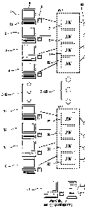
Figure 1 shows the high end KVM ("Keyboard-Video-
Mouse") computerized switching system or crosspoint switch
according to the present invenrion, which allows a larLye niunber of
computers to be coupled to a number of user terminals or
workstations. In the embodiment shown, 128 computers (201-328)
are interconnected with sixteen workstations (1-16), all computers
being accessible from any one of the workstations, which may be
remotely located in another room or building, for example. Each
workstation (1-16) comprises a user interface includinQ a video
monitor (1 a), a keyboard (1 b) and a cursor control device such as a
mouse (1 c). Workstation input signals from the keyboard and the
mouse are received by a user interface module (17-32), for
example, a known system called 4xP, by Cybex Computer Products
International Ltd-
2o The user interface module (17), packs and transmits;'receives
the bi-directional keyboard and mouse data signals over a
communication link (33) to/from a switching hub (40). After being
routed through the switching hub, the keyboard and mouse signals
are retransmitted on another communication link (50) to a comptiter
interface module (51) which is connected to a remotely-located
CA 02657977 2009-01-29
14
computer (201). The computer interface module may also of known
design, preferably a CvbeY 4xP. The computer interface module
separates and unpacks all the different types of data again and
supplies the keyboard and mouse signals through appropriate
connectors (180) to the input ports of the computer. The computer
interface module acts like a keyboard and mouse connected to the
computer even when communication with the workstation svstem is
lost. The emulation of keyboard and mouse at the computer
interface module also lets the computer boot without error messages
and failures.
The switching information needed for the switching hub
switch is usually generated in the user interface module (17 ). The
information is provided to the switching hub (40) by the
communication link (33), which already carries the mouse and
keyboard data signals.
Analogue video signal output produced by the remote
computer (201) is transmitted along the communication link (50) to
the switching hub (40). This is then routed through the switching
hub (40) and retransmitted to the user interface module (17), which
provides the video signals to the monitor (la).
Synchronization signals, horizontal sync (HS) and vertical
sync (VS) associated with the analogue video signals (e.g., red,
green, blue), are transmitted to the switching hub (40), routed
through the crosspoint switch arrangement, and then retransmitted
to the user interface module (17). The user interface module then
provides the synchronization signals to the monitor (la).
CA 02657977 2009-01-29
From a user's perspective, the monitor (la), keyboard (1 b)
and mouse (1 c) appear as if they are directly connected to the
remote computer (201).
5 The Switching Hub
Figure, 1 also shows in general outline a block diam-am of the
switching hub (40), which has many novel features in accordance
with the present invention. This is easily scalable to the needed
system, because of its physical modular architecture. Sk,~ itch
10 modules (41) fitting within indiVidual racks in the switching hub
(see Figure 6) housing each proVide access either to sixteen user
interface modules (17-23) or sixteen computer interface modules
(51-67) of the system. Each switch module is split into an analogue
card (42, 43) and a digital card (44), in a back to back
15 configuration. The switch modules are not all identical, and may be
configured either as a receive module (42, 44) or as a transmit
module (43, 44). The digital card (44) is most preferably common
for both types of switch module, which reduces design and
manufacturing costs. The analogue card is either an analogue
receiver (42) or analogue transmitter (43), adapted respectively to
distribute incoming or outgoing video signals from the switching
hub (40). A combined analogue receiveritransmitter card is
possible. The digital card handles video synchronization signals,
the external communication, and the control signals for the analogue
cards. Control signals coming from the digital card and going to the
analogue card are isolated with opto couplers.
CA 02657977 2009-01-29
16
There are therefore sixteen video channels per switch module
(41), in the embodiment described. The number of users or
computers could be increased with every module (41) by steps of
sixteen. This system will allow sixteen users to control 128
computers in a non-blocking wav. It is also possible to have more
than sixteen,user interfaces connected to the switching hub.
Additionally, it must be noted, more than one user can be connected
to the same computer.
Every switch module includes a sixteen bv sixteen digital
crosspoint switch arrangement (see Figure 2) and has access to
sixteen channels on a backplane (45). A "channel" comprises
different lines for each of the followinQ signals: analogue video red,
analogue video green, analogue video blue, a pair for vertical
synchronization (VS) and a pair for horizontal synchronization
(HS). Communication between the cards is performed on an
internal communication bus. This communication is based on a
differential CAN (controller area network) bus (404). For example,
information sent on the CAN bus may be keyboard information,
mouse information, switching information, system information,
update information for the main CPU, update information for the
programmable logic devices, control information.
Control panel
A control panel (46) may be used for updating the whole
system. The update information is distributed via the CAN bus
internally to other plugged cards and the external communication
CA 02657977 2009-01-29
17
bus distributes this information to other units, for example user
interface modules or computer interface modules. Another use of
the control panel is to configure the system and do administrative
work. The control panel could also be used for debugging the
system, e.g. from workstation (47).
Digital card
As mentioned above one switch module (41) con-sists of a
digital card (44) and one analogue transmitter (43) or rec.-iver (42)
card. The CPU (400) (central processing unit) shown in FIG.2
controls both cards, the digital and the analogue card. The analogue
card either transmits, or receives and switches the analooae video
signals. In contrast to this the digital card controls and distributes
the digital data signals, which are necessary for mouse, keyboard
and monitor switching. A defined interface controls the analogl.ie
card.
Central Processing Unit (CPU) and Memory
Distributed control is provided by a separate stand alone -
CPU and memory on each digital card. The CPU (400) on the
digital card is, for example, a sixteen bit CMOS microcontroller
(C167) from Siemens A.G. It uses a ROM (read onlv memory), a
RAM (random access memory) and a Flash ROM. For the memory
system (401), two of each (PAN1 and ROM) are used. The memory
devices are 8 bits wide, so one device is used for the lower and one
is used for the upper 8 bits of the 16-bit data bus. Everyrythimg in the
CA 02657977 2009-01-29
18
system is flash upgradeable. So the system or CPU starts up from a
Boot ROMIEPROM, but first looks for a newer firmware version in
the flash memory. If a newer version exists, the system goes on
executing commands from the flash memory. The flash ROM can
be updated on the card, through the system from a workstation (47),
from a remote computer, or from the control panel (46). for example
via an infrared link from a portable computer.
It is possible to use another processor type from this family.
By changing two resistors connected to the EA pin of the CPU, it is
possible to use a processor with internal flash and leave out the
flash ROM's from the memory system. There is an interface on the
digital card (44), which can be used for such an upgrade.
Programmable Logic Device and Transmitter/Receivers
During start-up the central processing unit progra.ms a
programmable logic device, or FPGA (402) in this embodiment,
programmed over a serial interface. This device is connected to the
data, address and control bus of the CPU. Programming this device
by the CPU on every start-up makes sure that there is always the
latest firmware in the FPGA.
To get a 16-channel communication to other units, four quad
UARTs (403) are used on every module (41). These UARTs are
also connected to the CPU data, address and control bus. Buffers
may be used for driving such an amount of devices on the address
bus.
CA 02657977 2009-01-29
19
The digital cards are fully bi-directional, i.e. all the input and
output signals can be reversed by direction controller (408) (see
Figure 3), and a common card is used for a transmitter (43, 44) and
a receiver (42, 44) switch module (41). The digital part (44) of the
module recognizes in what way it has to act depending on one
direction signal coming from the analogue part. When acting as a
receiver module, the synchronization signals HS, VS, come in from
the computer interface module (5 1) differentially. They are
received by differential line receivers and converted into CMOS
compatible signal levels. All sixteen HS and sixteen VS signals are
then connected to the FPGA.
Crosspoint Switches on Digital Card
There are two bi-directional 16 by 16-crosspoint switches
embodied by the FPGA (402). Both are switched simultaneously
for distributing HS and VS synchronization signals always together
on one channel or communication link. These crosspoint switches
are controlled by the CPU (400). The logic device is accessed by a
data bus (406), an address bus (405) and some control signals
(407). This interface is compatible to a standard microcontroller
interface. A serial control link could also be used.
Figure 3 shows the FPGA (402) and crosspoint switch
arrangement in more detail, which comprises from sixteen (16 bv 1)
multiplexers (450-466) for the HS and from sixteen (16 by 1)
multiplexers (470-486) for the VS synchronization signals. The
sixteen inputs of each group of multiplexers are connected together.
CA 02657977 2009-01-29
The outputs of the multiplexers go out of the device again. With
this arrangement, two 16 by 16 crosspoint switches are tiene rated.
When a connection is demanded by a user interface module,
the CPU (400) selects one of the sixteen multiplexers with its
5 coding on the address bus. The data bus will carry the information
which one of the sixteen inputs will forward to the output of the
multiplexer. There is one 5-bit data register for everv pair of
multiplexer (HS and VS), which stores the switching information
and keeps the connection. Data registers (409) are updated with
10 information from the data bus (406), when the address re-m'ster
recognizes a legal address and an update signal is sent to the
corresponding data register. Connections could be released in the
same way with the data bus on a low level on every signal. The
switching information is stored in the FPGA (402) when the device
15 is selected with the chip-enable signal and the write signal yoes low-
and rises again. The reset line will clear all connections_ It is the
same when the system is powered up again. The FPGA is
programmed by the CPU (400). It will be automatically updated
when the firmware of the CPU is updated.
20'
Low Voltage Differential Transceivers (LVDS)
When the synchronization signals are routed through the
crosspoint switch (402) they are routed to sixteen transceivers.
These low voltage differential signal (LVDS) transceivers (410)
provide the synchronization signals to the backplane (45). In this
embodiment, a LVDS transceiver is used because of reduction on
CA 02657977 2009-01-29
21
electromagnetic interference (EMI) and also to keep the crosstalk
between these and other signals low. The LVDS driver could be
reversed with the direction signal provided bv the analogue card.
In the reverse direction, when the digital card (44) acts like a
transmitter, the LVDS transceiver (410) receives differential
synchronization signals from the backplane, converts them into
CMOS compatible signal level and forwards them to the FPGA
crosspoint switch (402). This device will route the signals as
needed for the user and outputs them to a CATS (Category 5
1 o computer network cable) driver output section (411) again. These
differential drivers (See FIG.2) are in parallel to the receivers for
the reverse direction and are controlled by the direction si-nal
coming from the analogue card. There is only one of the parallel
drivers active at one time. The differential input or output from the
CAT5 side are connected to the differential line receiver of the type
26C32 and are also connected to the differential line driver of the
type 26C31. The signal T,,R (transmit/receive) determines the
direction information. The driver is active when this signal is on a
low level because it is connected to the positive enable pin of the-
driver. The T/R signal is also connected to the low active enable
signal of the differential line receiver and in case of an active driver
this receiver will be inactive and vice versa.
Communication Links
The external system communication is based on differential
signals. The previously prepared data packages, as prepared by the
CA 02657977 2009-01-29
22
user or computer interface modules (17, 51) are received by
differential line receivers at the CATS cable inputs. It should be
noted that this communication is based on a"full duplex proprietary
communication protocol.
Universal Asynchronous Receive Transmit Modules (UARTs)
Incoming data packages are converted to a CMOS-
compatible signai level and then forwarded to the UART (403)
inputs. For the sixteen communication links, four quad UARTs
(403) are used. These UARTs are full duplex as well, and transmit
and receive at the same time. The serial data is converted into
parallel data and stored in a FIFO (first in first out) memory. The
UART incorporates a 16-byte FIFO for every communication path.
The CPU, which is connected to the UARTs via data, address and
control buses (405, 406, 407) then has access to these bytes. The
CPU will be informed by interrupt signals when bytes arrive. The
UARTs will also report reception errors or transmission errors to
the CPU (400).
In the reverse direction, when the digital card (44) acts like a
transmitter, the CPU stores data bytes for external bus transmission
in the UART. These data bytes are serialized and output to the
CATS driver section (411) by the UART. To access the UARTs,
the data bus and the address bus are used. To generate the 16-chip
select signal, only one chip select signal is used from the CPU. The
others are generated by an address decoder (412) which is built up
from two 1 by 8 demultiplexers (See Figure 3). Therefore three
CA 02657977 2009-01-29
23
lower address lines are connected to the UARTs themselves and
four additional higher address lines are connected to the decoder
devices. The driver converts the CMOS signal into a differential
signal and outputs it to the CATS connectors.
The CPU which receives and transmits all the data from and
to the UARTs forwards all information with other destinations to
the internal system bus which is located on the backplane (45).
This system bus is based on the CAN bus. The integrated CAi~1
module (404) of the CPU is used for this. All serial CAN data is
output to a dedicated CAN driver (413) which converts the signals
into differential signals. The CAN system bus runs at a speed of
lmhz, for example. In this way all the modules communicate with
each other.
Handling of the CAN bus protocol
CAN bus data packages which are for a particular module are
handled by the CPU in that module. In case of switching
information it will send switching commands to the FPGA
crosspoint switch (402), to the analogue video crosspoint switch
(501, 502) and enable signals to the video buffers. For enabling the
video buffers a serial synchronous interface (500) is used. This
interface (500) to the respective analogue card (42, 43) is separated
by optocouplers to prevent noise on the analogue card. This serial
data is converted into sixteen parallel enable signals for the video
buffers. The six video crosspoint switches are controlled in the
same way. The serial synchronous data is clocked into the
CA 02657977 2009-01-29
24
crosspoint switches. This interface is also opto-isolated to prevent
high frequency digital noise in the analogue portion of the system.
Front Control Panel
The front control panel (46) which is also connected to the
internal CAN bus (414) will provide configuration information to
the switch modules. This could be information like memory update
information for the CPUs of the other switch modules (41). The
chassis address for this unit could be set with the control panel and
it will be forwarded to other cards which need the information.
The front panel (46) could also be used as an interface for
debugging the system. In this case the panel may be used to
monitor the internal communication bus (CAN) and forward the
information to a displav or to a computer (47) connected via serial
port to the panel. If needed the developer or user can read in or
send out commands and data.
The control panel may also be used to monitor the primary
and redundant power supply units (601, 602), and -1jive a warning of
voltage drops or power failures. It may also be used for monitonng
the temperature in the system housing and will give an alarm in the
case of overheating.
The user interface of the control panel may be a graphic
display with a touch panel to enter commands and set up the
system, or a character display with buttons or switches to enter
information.
CA 02657977 2009-01-29
Redundant power supplies
The system most preferably includes two independent, fully
redundant power supply units. If one power supply (601) fails the
other one (602) will guarantee a stable system which will go on
5 working without interruption. The power supplies are monitored bv
the control panel.
Hot Swap
Every replaceable module in the system is most preferably
10 designed to be -'hot swappable". Every single module, e. g. power
supplies (601, 602), fan modules (603, 604), all switch modules
(41), and the control panel (46), could be plugged or unplugged in a
powered on condition without interruption of svstem fiinction. The
novel modular design of the switch modules (41) allows each of
15 these to be individuallv hot-swappable, a most advantageous feature
of the invention.
Analogue Transmitter Card (Fig. 4)
The transmitter switch module (43, 44) consists of an
-
20 analogue transmitter card (43) "stacked" on top of the digital card
(44), as described above. Each input stage of the transmitter card
presents a high impedance to the backplane analogue bus thereby
causing negligible loading and maximizing signal integrity.
The analogue transmitter card is connected to the backplane
25 analogue bus using, for eYample, aHIDM plus daughtercard
connector assembly (503), as supplied by Teradyne Inc.
CA 02657977 2009-01-29
26
The length of the printed circuit board (PCB) track between
the connector and the input buffer amplifier (504) has been kept as
short as possible in order to minimize stray parasitic capacitance
and thereby maximize channel bandwidth. The output of this
amplifier directly drives (i.e. the transmission line is onlv terminated
at the far end by its characteristic impedance) a controlled
impedance transmission line implemented by a stripline structure
embedded in the PCB structure during manufacture. This stripline
has a nominal impedance of 50Q +/ - 15%. The termination for
this section of stripline is placed as close as possible to a 16 X 16
analogue crosspoint switch, which may comprise two 16 X 8
Buffered Video Crosspoint Switches (501, 502) per analogue signal
(red, green, blue), for example, product part AD8110 by Analog
Devices, Inc. In order to build a 16 X 16 non-blocking matrix the
sixteen single-ended high impedance inputs of both devices are
connected in parallel thus forming a 16 X 16 crosspoint matrix
switch. Therefore to implement a 16 X 16 non-blocking crosspoint
matrix for all three analogue signals (red, green, blue) requires six
AD8110 devices (501, 502) in this embodiment of the invention. -
Control signals from the corresponding and adjacent digital
card (44) in the switch module (41) are supplied to the analogue
transmitter card (43) as serial data via a stacker connector. In order
to minimize the coupling of conducted digital "noise" from the
digital card to the analogue circuits all control signals are
"galvanically isolated" using opto-isolators (500), in a known
manner. On the analogue side of the opto-isolated barrier this serial
CA 02657977 2009-01-29
27
data stream is fed directly to the analogue crosspoint switches and
determines the signal routing within the crosspoint switch. The
selected active crosspoint output is buffered immediately by a
wideband monolithic amplifier (505)_ This buffer directly drives a
section of "stripline" similar to that described earlier.
This s,tripline section carries the routed signal to a correctly
terminated input stage of discrete differential amplifier stay7e (506).
This differential amplifier stage provides the single-ended to
balanced conversion. This stage also provides switched "pre-
emphasis". The pre-emphasis applied here in conjunction with the
equalization in the analogue receiver provides a means to
accommodate a wide range of CATS cable lengths. The balanced
signal is connected to the respective RJ45 by a section of balanced
stripline with a nominal 100SZ differential impedance.
Method of Operation of the Backplane Analogue Bus
Controlled impedance "stripline" techniques have been used
in the design of the analogue video bus portion of the backplane in
order to optimize signal integrity, channel bandwidth and crosstalk
separation. The analogue backplane bus consists of sixteen
"Double Matched" transmission lines, (i.e. terminated at both ends
by its characteristic impedance) implemented in a"stripline"
structure with a loaded impedance of approximately 50Q. Thus the
effective input impedance at any point along this transmission line is
25Q.
CA 02657977 2009-01-29
28
The analogue bus driver device in the receiver card drives
this backplane with a nominal 25Q source impedance. This
matched impedance approach minimizes ringinna on fast signal
edges, (See Figure 8).
Adjacent channel crosstalk is reduced bv interleaving
adjacent chatuiel paths in an alternate tri-plate stripline structure,
i.e. all even channels are carried in one stripline structure and all
odd channels are carried in another offset structure_ Expanding on
the above technique additional stripline structures mav be used to
lo further enhance the separation between channels thus further
improving the crosstalk separation, (See Fiipare 9).
In order to maintain maximum system bandwidth and optimal
crosstalk separation, special consideration has been given to the
choice of interconnect technology employed. The connector chosen
is preferably from the FIDhT plus range manufactured bv Teradyne,
Inc. This connector has an integral stripline structure and is
optimized for controlled impedance environments between 500 and
600. A specific pin assignment is used with this connector in order
to maximize the crosstalk separation between channels, (See Figure
2o 7).
This pin assignment creates a "pseudo -c o axial cavitv" (700)
defined by ground pins (701) surrounding each analogue signal path
(702) within the mated connector body therebv resultina in optimal
crosstalk separation.
CA 02657977 2009-01-29
29
Analogue Receiver Card (Fig. 5)
The receiver switch module (42, 44) consists of an analogue
receiver card (42) "stacked" on top of the digital card. Red, green,
blue and HS synchronization irlformation are presented to the
analogue receiver card as electronically balanced or differential
signal pairs., VS synchronization information, along with kevboard
and mouse signals are routed directly to the digital card (44)
underneath. Each channel or above signal group are accommodated
in one CAT 5 cable assembly terminated in an RJ 15 connector.
The balanced HS synchronization signal is directly routed internally
to the digital card via the stacker connector. The analoo--Lie receiver
does not perform any operation on this signal.
The remainina differential red, blue and green sivnals are
routed from the RJ4S connectors to the input stages bv balanced
stripline with a nominal 100SZ differential impedance, where they
are converted to single-ended signals by discrete differential
amplifier stages (509). Each differential amplifier incorporates
switched cable equalization in order to compensate for the
progressive high frequency roll-off with increasing length of CATS
cable used and therefore "flatten" the frequency response.
In order to reduce power consumption inactive or unused
differential amplifier input stages have powerdown capability
whereby the power supply voltage is removed from the stage. This
also reduces internal heat produced from unused input stages that
are turned on.
CA 02657977 2009-01-29
The control signals required to provide the enable; disable
function are derived from the serial data stream. This control
information is extracted using two 8-bit shift registers and controls
the discrete input differential amplifier stages directly.
5 The output signal is then buffered bv a monolithic amplifier
(508) whose output directly drives (i.e. the transmission line is only
terminated at the far end by its charactenstic impedance) a
controlled impedance transmission line implemented by a stripline
strt.icture embedded in the PCB structure durinu manufacture. This
10 stripline has a nominal impedance of 50Q -~- 15%. The
terrnination for this section of stripline is placed as close as possible
to the 16 X 16 analogue crosspoint switch (501, 502), similar to that
described above for the transmitter card.
A crosspoint switch topology based on "switched
15 transconductance architecture" has been chosen over the more
common "bilateral mosfet switch" type of device. The particular
crosspoint switch used consists of an array of 1218 transconductance
input stages organized as eight 16:1 multiplexers with a common,
16-line analogue input bus. Each multiplexer is basicallv a folded-
20 cascode high-speed voltage feedback amplifier with sixteen input
stages. This architecture results in a low-power large matrix
crosspoint switch with high input resistance, low input capacitance
and wide bandwidth without the use of additional input buffers.
Therefore to implement a 16 X 16 non-blocking crosspoint
25 matrix for all three analogue video signals (red, green, blue)
requires six AD81 10 devices in the present implementation of the
CA 02657977 2009-01-29
31
invention. Control signals from the digital card underneath are
supplied to the analogue receiver PCB as serial data via the stacker
connector. In order to mn
iimize the coupling of conducted digital
"noise" from the digital PCB to the analogue circuits all control
signals are "galvanically isolated" using opto isolators. On the
analogue side of the opto-isolated barrier this serial data stream is
fed directly to the analogue crosspoint switches and detennines the
signal routing within the crosspoint switch. The selected active
crosspoint output is buffered immediately by a wideband monolithic
amplifier (511). This buffer directly drives a section of --stripline"
similar to that described earlier. This stripline section carries the
signal to the correctlv terminated input stage of the 'backplane
analog bus" driver circuit (510) located close to the HDM plus
daughtercard connector (503). This placement is necessarv in order
to keep the unterminated "stub" length short when the bus dnver is
disabled. The analogue transmitter card (42) is connected to the
backplane analogue bus using a HDM plus daughtercard connector
assembly, as described above.
In the present embodiment of the invention the analogue bus
driver used is a MAX4223EUT-T device, supplied bv Maxim. This
device has an output disable function which is activated bv
"pulling" a shutdown control pin (SHDN) low (507).
Therefore a particular channel output is effectivelv "wire-
OR'ed" with the same channel outputs on another receiver card or
cards in the same chassis thereby giving each card's output access
to the common backplane analogue bus. The control signals
CA 02657977 2009-01-29
32
required to provide the enable/disable function are also derived
from the serial data stream. This control information is extracted in
a similar manner to that described for the differential input stages
using a further two 8-bit shift registers and controls the analogue
bus drivers directly.
While the invention has been particularly shown and
described with reference to embodiments thereof, those skilled in
the art will understand that the foregoing and other changes in form
and detail may be made therein without departing from the spint
1 o and scope of the present invention.