Note: Descriptions are shown in the official language in which they were submitted.
CA 02658187 2009-01-19
WO 2008/009074 PCT/BE2007/000083
1
Compact catadioptric spectrometer
Technical field of the invention
The present invention relates to the field of optical detection. More
particularly, the present invention relates to methods and systems for
optically
characterising materials, e.g. using spectroscopic measurements.
Background of the invention
In a large number of today's applications, such as for example
biotechnology applications or material characterisation, spectroscopy is used
as a routine tool for performing absorbance and fluorescence and Raman
measurements. For example in bio-sensing applications, molecular diagnostics
or pharmacological applications, often a number of samples are processed in
parallel, in order to increase the processing speed. An example of so-called
high-throughput screening is the application of multi-well plates with a high
number of sample reservoirs, ranging from 96 to 384 and even higher.
With the increasing number of wells in these plates, processing a whole
plate in a serial way becomes too time-consuming and a parallel way of
processing becomes necessary. The most obvious way to conduct a
spectroscopic measurement on several samples simultaneously is to provide
each sample with its own spectrometer. Even the smallest spectrometers
available today will make such a setup rather large and difficult to assemble.
Various samples can also be studied simultaneously by using hyperspectral
imaging, in which, typically a one-dimensional image is transformed into a two-
dimensional spectral image. When there is a minimal distance between two
samples such a setup results in a poorly filled field of view of the
hyperspectral
imager and the hyperspectral imager must be dimensioned for the entire
sample row, making the imager large.
In a classic Czerny-Turner configuration, typically one mirror is used to
collimate light coming from an entrance slit and direct it towards the
reflection
grating. After diffraction, a second mirror is used to focus the light onto
the
detector or an exit slit. Sometimes both mirrors are combined into one mirror
in
which the configuration is also called an Ebert-Fastie configuration.
CA 02658187 2009-01-19
WO 2008/009074 PCT/BE2007/000083
2
US Patent 6,862,092 B1 describes a system and method for measuring
spectral information of light from at least one object. The system describes
the
use of a transparent body, whereby a light beam enters the transparent body
and guides the diverging light beam via two mirror reflections on a
diffractive
optical element. The diffracted light beam then is reflected at an aspheric
mirror surface and is directed to a detector element 34, allowing to detect
spectral information. The transparent body typically has a complex, non-
standard lens shape.
Summary of the invention
It is an object of the present invention to provide good apparatus or
methods for optical characterisation of materials. It is furthermore an object
of
the present invention to provide components thereof, assisting in good optical
characterisation of materials.
The above objective is accomplished by a method and device according
to the present invention.
The present invention relates to an optical characterisation system for
characterising material, the system comprising a diffractive element, a
detector
and an optical element, the optical element adapted for receiving at a first
side
of the optical element an illumination beam after interaction with the
material to
be characterised, the optical element having a refractive surface for
refractively
collimating the received illumination beam on the diffractive element and the
optical element having a reflective surface for reflectively focussing the
diffracted illumination beam.on the detector, the diffractive element and the
detector being at a same side of the optical element, opposite to said first
side.
The refractive surface and reflective surface may be positioned at the same
side of the optical element. It is an advantage of such embodiments according
to the present invention that a compact optical characterisation system can be
obtained. It is furthermore an advantage of such embodiments according to the
present invention that a compact system for spectroscopic measurements is
obtained. It is an advantage of such embodiments according to the present
invention that a system with limited manufacturing effort can be obtained. It
is
CA 02658187 2009-01-19
WO 2008/009074 PCT/BE2007/000083
3
an advantage of such embodiments according to the present invention that the
amount of stray light from light incident on the optical element and directly
reaching the detector is limited, without putting a high burden on the
manufacturing of the optical component. The refractive and the reflective
surface may be different parts of the same curved surface of an optical
element. The refractive surface may be a part of a curved surface of an
optical
element not comprising reflective material and the reflective surface may be a
part of a curved surface of an optical element being made reflective, e.g. by
coating with reflective material. It is an advantage according to the present
invention that the optical element can be used in a configuration wherein the
sample can be provided at an appropriate position from the optical element
such that an efficient and sensitive system can be obtained. A surprisingly
compact system being at the same time sensitive and readily easy to
manufacture thus was obtained.
The optical element may be adapted for receiving a diverging
illumination beam.
The diffractive element and the detector may be in contact with the
optical component. It is an advantage of such embodiments according to the
present invention that a system requiring limited manufacturing effort can be
obtained. It furthermore is an advantage of such embodiments according to the
present invention that the number of optical reflections in the system are
low,
resulting in less losses, and less stray light.
The receiving side of the diffractive element and the receiving side of
the detector may be positioned in the same plane. It is an advantage of such
embodiments according to the present invention that a rigid system can be
obtained. It is an advantage of such embodiments according to the present
invention that a relatively easy manufacturing is obtained. It is also an
advantage that the outlining of components is made more easy as outlining
only needs to be performed in two directions instead of three.
The optical element may be a catadioptric element. It is an advantage of
such embodiments according to the present invention that the collimation and
focusing can be done by a single optical element. It is an advantage of such
embodiments according to the present invention that the number of optical
CA 02658187 2009-01-19
WO 2008/009074 PCT/BE2007/000083
4
elements needed is limited. It is furthermore an advantage of such
embodiments according to the present invention that the optical element is a
standard optical component. The collimation may be performed prior to the
focusing. It is also an advantage of such embodiments according to the
present invention that the number of components needed may be reduced
compared to a classic Czerny-Turner configuration.
The optical element may be a partially coated piano-convex spherical
lens element. It is an advantage of such embodiments that the single optical
element may be made by partially coating a normal multi-purpose lens. The
coating may be a reflective coating.
At least one of the refractive surface or the reflective surface may have
a mirrored portion on the other surface, i.e. said reflective surface
respectively
refractive surface. The mirrored portion may be a mirror-symmetric portion. It
is
an advantage of embodiments of the present invention that a lens with a
continuous lens surface can be used. The latter may allow the lens to be made
using conventional lens manufacturing techniques, without the need for
reshaping the optical element substantially, e.g. by removing part of the lens
volume. The at least part of the refractive surface may comprise at least the
surface actively used for refracting.
The optical characterisation system may be adapted for using an
illumination beam having a continuous spectrum or quasi-continuous
spectrum. It is an advantage of such embodiments according to the present
invention that spectroscopic measurements may be performed, resulting in
broad spectral information about the material to be characterised. The latter
allows for example characterisation/detection of a plurality of elements in
the
material to be characterised.
Any of the diffractive element may be formed on a surface of the optical
element. The detector may be positioned adjacent to the optical element. It is
an advantage of such embodiments according to the present invention that a
robust and/or shock-resistant system may be obtained. It is also an advantage
of such embodiments according to the present invention that the accuracy of
the systems may be improved, as the amount of positioning and alignment
CA 02658187 2009-01-19
WO 2008/009074 PCT/BE2007/000083
needed is reduced. In other words, the number of alignments between
components that need to be taken care of may be reduced.
The number of reflections of an incident illumination beam in the optical
element may be two or less. If interaction with the diffractive element is not
5 counted as a reflection, the number of reflections of an incident
illumination
beam in the optical element may be one. The latter leads to a high resolution.
The optical element may be adapted such that an incident illumination
beam is incident on the diffractive element under an angle, and wherein the
detector is furthermore adapted for detecting a specular reflected zeroth
order
of the illumination beam. It is an advantage of such embodiments according to
the present invention that detection of a specular reflected zeroth order of
the
illumination beam allows to use this zeroth order of the illumination beam for
alignment or for post-processing of the measured results, such as e.g. for
taking the power of the illumination beam into account.
The optical characterisation system may be a multi-channel
spectrometer. The optical characterisation system may be a multi-channel
optical characterisation system adapted for characterising a plurality of
samples in parallel, e.g. in different channels in the system.
The optical element may be a first piano-convex lens being at least
partially transiationally invariant in a first direction. It is an advantage
of such
embodiments according to the present invention that multiplexing may be
performed with a compact system, i.e. that several samples can be measured
simultaneously.
The diffractive element of the optical characterisation system may be a
diffractive element common to different channels of the multi-channel optical
characterisation system, e.g. spectrometer.
It is an advantage of such embodiments according to the present
invention that the number of components used for the optical characterisation
system may be limited.
The detector of the optical characterisation system may be a detector
common to different channels of the multi-channel optical characterisation
system, e.g. spectrometer. It is an advantage of such embodiments according
CA 02658187 2009-01-19
WO 2008/009074 PCT/BE2007/000083
6
to the present invention that the number of components used for the optical
characterisation system may be limited.
The optical characterisation system may comprise a sample holder for
positioning the sample at a distance from the optical element, the distance
being between one time a radius of curvature of the refractive surface and
four
times a radius of curvature of the refractive surface.
The optical characterisation system furthermore may comprise, for each
channel, a second plano-convex lens for focussing or collimating the
illumination beam in the channel in the direction wherein the first plano-
convex
lens is translationally invariant.
The optical element may be adapted for receiving an illumination beam
at a first side of the optical element, and the diffractive element and the
detector are positioned at a single, second side of said optical element, the
second side being opposite to the first side.
The present invention also relates to a method for optically
characterising a material, the method comprising illuminating a material with
an
illumination beam thus generating an illumination response, thereafter,
refracting at a first side of an optical element the illumination response
from the
sample into a collimated illumination response at an optical element,
diffracting
the collimated illumination response thus generating a diffracted illumination
response, reflecting, at the optical element the diffracted illumination
response
thus generating a reflected illumination response, and detecting said
reflected
illumination response at a same side of the optical element as said
diffracting
the illumination response, the same side being opposite to said first side of
the
optical element.
The present invention furthermore relates to an optical element adapted
for receiving at a first side of the optical element an illumination beam and
adapted for being used with a diffractive element and a detector, the optical
element having a refractive surface for refractively collimating the received
illumination beam on a diffractive element and the optical element having a
reflective surface for reflecting the collimated diffracted illumination beam,
diffracted by the diffractive element, on a detector, said optical element
being
adapted for the diffractive element and the detector to be positioned at a
same
CA 02658187 2009-01-19
WO 2008/009074 PCT/BE2007/000083
7
side of the optical element. The optical element may be adapted for receiving
a
diverging illumination beam and provide the further functionality as described
above.
The optical element may be a catadioptric element.
The optical element may be a partially coated lens element.
The refractive surface and the reflective surface may be part of the
same convex surface of the optical element. It is an advantage of
embodiments of the present invention that a lens made with conventional lens
manufacturing techniques can be used.
The optical element may be a plano-convex element.
The optical element may be adapted such that the number of reflections
of an incident illumination beam, to be detected by a detector, in the optical
element is two or less.
The optical element may be at least partially translationally invariant in a
first direction.
The optical element may be a plano-convex cylindrical lens.
At least one of the refractive surface or the reflective surface may have
a mirrored portion on the other surface, i.e. said reflective surface
respectively
refractive surface. The mirrored portion may be a mirror-symmetric portion. It
is
an advantage of embodiments of the present invention that a lens with a
continuous lens surface can be used. The latter may allow the lens to be made
using conventional lens manufacturing techniques, without the need for
reshaping the optical element substantially, e.g. by removing part of the lens
volume. The at least part of the refractive surface may comprise at least the
surface actively used for refracting.
The present invention also relates to a computer-based method for
designing an optical characterisation system for characterising material, the
system comprising a diffractive element, a detector and an optical element,
the
optical element adapted for receiving an illumination beam after interaction
with the material to be characterised, the optical element having a refractive
surface for refractively collimating the received illumination beam on the
diffractive element and the optical element having a reflective surface for
reflectively focussing the diffracted illumination beam on the detector, the
CA 02658187 2009-01-19
WO 2008/009074 PCT/BE2007/000083
8
method comprising receiving parameters about the optical element and the
diffractive element, for at least one relative position of the optical element
with
respect to the diffractive element, determining a position of a focus curve
for
an illumination beam focused by the optical element, and evaluating said
position of said focus'curve with respect to a position of a detector surface
of
the detector, positioned at a same side of the optical element as the
diffractive
element.
The invention also relates to a computer program product that, when
executed on a computing means, is adapted for performing such a computer-
based method for designing. It furthermore relates to a machine readable data
storage device storing such a computer program product and transmission of
such a computer program product over a local or wide area
telecommunications network.
Particular and preferred aspects of the invention are set out in the
accompanying independent and dependent claims. Features from the
dependent claims may be combined with features of the independent claims
and with features of other dependent claims as appropriate and not merely as
explicitly set out in the claims.
Although there has been constant improvement, change and evolution
of devices in this field, the present concepts are believed to represent
substantial new and novel improvements, including departures from prior
practices, resulting in the provision of more efficient, stable and reliable
devices of this nature.
The teachings of the present invention permit the design of improved
methods and apparatus for optical characterisation of materials, such as for
bio-sensing or material characterisation.
The above and other characteristics, features and advantages of the
present invention will become apparent from the following detailed
description,
taken in conjunction with the accompanying drawings, which illustrate, by way
of example, the principles of the invention. This description is given for the
sake of example only, without limiting the scope of the invention. The
reference figures quoted below refer to the attached drawings.
CA 02658187 2009-01-19
WO 2008/009074 PCT/BE2007/000083
9
Brief description of the drawings
Fig. 1 is a schematic illustration of an optical characterisation system
according to embodiments of a first aspect of the present invention.
Fig. 2a is an exemplary illustration of an X-Z cross-section of part of an
optical characterisation system comprising a grating according to a first
embodiment of the first aspect of the present invention.
Fig. 2b is an exemplary illustration of an X-Y cross-section of part of an
optical characterisation system comprising a grating and a piano-convex
spherical optical element according to a first embodiment of the first aspect
of
the present invention.
Fig. 3 is an exemplary illustration of an X-Z cross-section of part of an
optical characterisation system comprising an immersed grating according to a
second embodiment of the first aspect of the present invention.
Fig. 4 is an exemplary illustration of an X-Z cross-section of part of an
optical characterisation system comprising a diffractive element and/or
detector adjacent the optical element, according to a third embodiment of the
first aspect of the present invention.
Fig. 5 is an exemplary illustration of an X-Z cross-section of part of an
optical characterisation system comprising an additional transparent plate
between the optical element and the diffractive element and/or detector,
according to a fourth embodiment of the first aspect of the present invention.
Fig. 6 is an exemplary illustration of an X-Z cross-section of part of an
optical characterisation system comprising wedge-shaped plates between the
optical element and the diffractive element and/or detector, according to a
fifth
embodiment of the first aspect of the present invention.
Fig. 7a is an exemplary illustration of an X-Z cross-section of part of an
optical characterisation system being a multi-channel optical characterisation
system according to a sixth embodiment of the first aspect of the present
invention.
Fig. 7b is an exemplary illustration of an X-Z cross-section as shown in
Fig. 7a, whereby the light path for radiation of one wavelength is shown.
Fig. 8 is an exemplary illustration of an X-Y cross-section of part of an
optical characterisation system being a multi-channel optical characterisation
CA 02658187 2009-01-19
WO 2008/009074 PCT/BE2007/000083
system according to a sixth embodiment of the first aspect of the present
invention.
Fig. 9 is an exemplary illustration of an X-Y cross-section of an
altemative part of an optical characterisation system being a multi-channel
5 optical characterisation system according to a sixth embodiment of the first
aspect of the present invention.
Fig. 10 is an exemplary illustration of a simulation result for an incident
light beam in an optical characterisation system as described in the first
aspect
of the present invention.
10 Fig. 11 is an exemplary illustration of a computing system as may be
used for performing a method for designing according to a further aspect of
the
present invention.
Fig. 12 is a schematic representation of the different angles between a
refracted illumination beam, a diffracted illumination beam and a reflected
illumination beam as can be used in the method for designing according to a
further aspect of the present invention.
Fig. 13 is a schematic representation of a determined focus curve, as
determined in a method for designing according to a further aspect of the
present invention.
Fig. 14 is a schematic representation of possible initial positional
conditions for determining a focus curve, as can be used in the method for
designing according to a further aspect of the present invention.
In the different figures, the same reference signs refer to the same or
analogous elements.
Description of illustrative embodiments
The present invention will be described with respect to particular
embodiments and with reference to certain drawings but the invention is not
limited thereto but only by the claims. The drawings described are only
schematic and are non-limiting. In the drawings, the size of some of the
elements may be exaggerated and not drawn on scale for illustrative purposes.
The dimensions and the relative dimensions do not correspond to actual
reductions to practice of the invention.
CA 02658187 2009-01-19
WO 2008/009074 PCT/BE2007/000083
11
Furthermore, the terms first and second and the like in the description
and in the claims, are used for distinguishing between similar elements and
not
necessarily for describing a sequential or chronological order. It is to be
understood that the terms so used are interchangeable under appropriate
circumstances and that the embodiments of the invention described herein are
capable of operation in other sequences than described or illustrated herein.
Moreover, the term under and the like in the description and the claims
are used for descriptive purposes and not necessarily for describing relative
positions. It is to be understood that the terms so used are interchangeable
under appropriate circumstances and that the embodiments of the invention
described herein are capable of operation in other orientations than described
or illustrated herein.
It is to be noticed that the term "comprising", used in the claims, should
not be interpreted as being restricted to the means listed thereafter; it does
not
exclude other elements or steps. It is thus to be interpreted as specifying
the
presence of the stated features, integers, steps or components as referred to,
but does not preclude the presence or addition of one or more other features,
integers, steps or components, or groups thereof. Thus, the scope of the
expression "a device comprising means A and B" should not be limited to
devices consisting only of components A and B. It means that with respect to
the present invention, the only relevant components of the device are A and B.
The following terms are provided solely to aid in the understanding of
the invention. These definitions should not be construed to have a scope less
than understood by a person of ordinary skill in the art.
The terms "optical" e.g. in optical system and "illumination" e.g. in
illumination beam typically may refer to visual, infrared or ultraviolet
radiation.
Nevertheless, the present invention is not limited thereto and also relates to
optical systems and components suitable for other types of electromagnetic
radiation. The term "transparent" typically refers to a property of a
construction
material of a component expressing that an illumination beam is not
substantially absorbed by the material, i.e. that preferably at least 50%,
more
preferably at least 80%, even more preferably at least 90%, still more
preferably at least 95% of the illumination beam is transmitted through the
CA 02658187 2009-01-19
WO 2008/009074 PCT/BE2007/000083
12
component. With an illumination beam having a continuous or quasi-
continuous spectrum there is meant an illumination beam comprising having
wavelengths within a wavelength range of the electromagnetic radiation
spectrum being substantially representative for that wavelength range. The
wavelength range may span over at least 10nm, more preferably over at least
50nm, still more preferably over at least 200nm, even more preferably over at
least 500nm.
Optical characterisation may comprise obtaining an "optical response"
or "optical detection signal" from a sample material. The latter may be
obtaining a transmitted or reflected portion of an illumination beam after
interaction with the fluid sample, which for example allows to see a change in
intensity and or spectral behaviour due to absorption by the fluid sample or
particular analytes therein. Alternatively or in addition thereto, it may be
obtaining a luminescence response, such as e.g. a fluorescence response, of
a fluid sample or particular, optionally labelled, analytes therein as
response to
illumination of the sample fluid with the illumination beam. Labelling of
analytes
may be performed to detect presence of predetermined analytes by providing
labels to these analytes, e.g. radiative labels or fluorescent labels although
the
invention is not limited thereto. Such labels may be attached to the analytes
directly or indirectly.
Optical characterisation of the sample material may comprise optical
characterisation of solids, gasses or fluid samples as such or
characterisation
of specific analytes present in such samples, such as e.g. proteins,
antibodies,
nucleic acids (e.g. DNR, RNA), peptides, oligo- or polysaccharides or sugars,
small molecules, hormones, drugs, metabolites, cells or cell fractions, tissue
fractions, specific chemical components, etc. The latter may be detected in an
original sample fluid, or the sample fluid may already have been processed,
such as filtered, dissolved into a buffer, chemically or biochemically
modified,
diluted, etc. The sample material may be e.g. biological fluids, environmental
fluids, research fluids, fluids comprising solid sample material, solid
material
etc.
The invention will now be described by a detailed description of several
embodiments of the invention. It is clear that other embodiments of the
CA 02658187 2009-01-19
WO 2008/009074 PCT/BE2007/000083
13
invention can be configured according to the knowledge of persons skilled in
the art without departing from the true spirit or technical teaching of the
invention, the invention being limited only by the terms of the appended
claims.
In a first aspect, the present invention relates to an optical
characterisation system for characterising material. Typically such a
characterisation system may for example be used for material characterisation
or as bio-sensor, the invention not being limited thereto. The optical
characterisation system according to the first aspect comprises an optical
element for receiving an illumination beam, whereby the illumination beam
typically may have interacted with sample material to be studied. The
illumination beam received in the optical element typically may be an
illumination beam obtained after interaction with the sample material. . It
may
be an illumination beam wherein part of the spectrum is at least partially
absorbed or it may be a luminescence beam obtained after exciting the sample
material with an original illumination beam. The optical characterisation
system
furthermore typically comprises a diffractive element and a detector for
respectively diffracting different spectral components of the illumination
beam
differently and for detecting the illumination beam. According to the first
aspect
of the present invention, the optical element typically has a refractive
surface
for refractively collimating the illumination beam on the diffractive element
and
a reflective surface for reflecting the diffracted illumination beam on the
detector. The diffractive element and the detector thereby typically are
positioned at the same side of the optical element. The latter allows to
obtain a
compact optical system allowing to obtain spectroscopic information. Different
standard and optional components of such a characterisation system are
shown by way of illustration in Fig. 1, illustrating an exemplary optical
characterisation system 100 according to an embodiment of the present
invention.
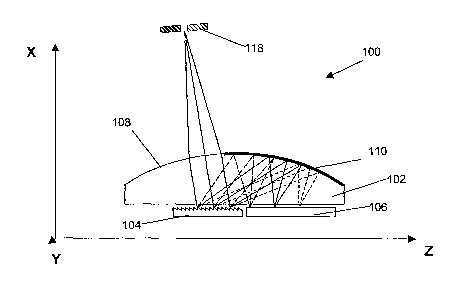
The optical characterisation system 100 typically comprises an optical
element 102 adapted for receiving an illumination beam, a diffractive element
104 and a detector 106. The optical element 102 typically may be substantially
transparent for the illumination beam. It may be a piano-convex optical
element. Typically, such an optical element 102 may be made from glass,
CA 02658187 2009-01-19
WO 2008/009074 PCT/BE2007/000083
14
silica, a polymer such as e.g. a plastic, etc. i.e. any suitable material
allowing
to obtain sufficient transparency. The optical element 102 typically may have
a
refractive surface 108 for refractively collimating the illumination beam on
the
diffractive element 104 and a reflective surface 110 for reflecting the
diffracted
illumination beam on the detector 106. The refractive surface 108 typically
may
be obtained by using a convex lens element, e.g. plano-convex lens element,
for the optical element 102. Furthermore, also the reflective surface 110 may
be obtained using the convex lens element. The refractive surface 180 and the
reflective surface 110 may be part of the same convex surface of the optical
element. The refractive surface or the reflective surface may be shaped such
that a mirrored portion thereof coincides with at least a portion of the other
surface, e.g. the reflective surface or refractive surface respectively. Such
a
mirrored portion also may be referred to as a mirror-symmetric portion. The
refractive surface or the reflective surface may be mirrored surfaces of the
optical element with respect to a mirror axis or mirror plane of the optical
element. The optical element may comprise a symmetry axis such that the
reflective surface is symmetric to the refractive surface with respect to the
symmetry axis. The curved lens surface may be spherical or may be any other
suitable shape. It may e.g. be a dedicated aspherical curved surface to
achieve improved focussing of all wavelengths in the plane of the detector.
The dedicated aspherical shape may e.g. be determined using optical
modelling software, such as Zemax available from Zemax Development
Corporation, LightToots available from Optical Research Associates,
TracePro available from Lambda Research Corporation or Advanced
Systems Analysis Program ASAP7N1 available from Breault Research
Organisation. The optical element 102 may be grinded, moulded or laser
ablated, computer numerical controlled turned or replicated in any suitable
way
from a master form into a specific form.
As described above typically part of the curved surface of the convex,
e.g. piano-convex, lens may act as refractive surface 108. For example, the
optical element 102 may be a plano-convex spherical lens element wherein
part of the spherical surface of the lens element acts as refractive surface
108
or it may be a piano-convex (partially) cylindrical lens element wherein part
of
CA 02658187 2009-01-19
WO 2008/009074 PCT/BE2007/000083
the cylindrical surface of the lens element acts a refractive surface 108. The
reflective surface 110 typically may be obtained by coating part of the
optical
element with a reflective material, such as e.g. with a reflective metal or
with a
reflective dielectric coating, e.g. a stack of thin films. Typically part of
the
5 curved surface of the plano-convex lens element may be coated with a
reflective material. Preferably a high reflection coefficient is obtained for
the
wavelength range of the illumination beam, such as e.g. a reflectivity of 80%,
preferably 90%, even more preferably 95%. Typically, in case the optical
element is a plano-convex spherical lens or a plano-convex cylindrical lens,
10 the partial coating of the optical element 102 may be a partial coating on
a
cylindrical surface or a spherical surface of the lens element. The optical
element 102 thus may act as a catadioptric element performing both the action
of refracting and reflecting. The optical element 102 may, e.g. in case a
multi-
channel optical characterisation system is envisaged, be an optical element
15 102 being at least partly transiationally invariant in one direction, such
as e.g. a
plano-convex cylindrical lens element. The optical element 102 may, in case a
multi-channel optical characterisation system is envisaged, be common to a
plurality or all of the channels of the optical characterisation system. It is
an
advantage of embodiments of the present invention that the optical element
can be made from a conventional or standard optical component, such as from
a convex, e.g. piano-convex lens element, without the need for reshaping the
optical element. The latter is advantageous to reduce the manufacturing effort
and allows to increase the accuracy and/or to reduce the number of
manufacturing errors than can be made as it avoids these additional
processing steps. In other words, a normal multi-purpose lens may be used as
optical element 102. The refractive surface 108 may allow to collimate
impinging illumination and bring a collimated illumination beam on the
diffractive element 104. The latter may allow to obtain a system wherein the
distance between subsequent optical components such as the refractive
surface 108, the diffractive element 104, the reflective surface 110 and the
detector 106 corresponds with the focus distance for the refractive or
reflective
surface, thus resulting in an accurate system.
CA 02658187 2009-01-19
WO 2008/009074 PCT/BE2007/000083
16
The diffractive element 104 typically may be a grating. Such a grating
may be ruled or holographic. It may have a symmetric shape, e.g. a sinusoidal
shape, a blazed shape, e.g. a saw-tooth profile or a shape in between those
two forms. It may also comprise a stepped saw-tooth profile. The grating can
e.g. be made in the bottom side of the optical element 102 or it may be a
separate component. It may be covered with a reflection layer. The grating
may e.g. be made using grooving ruling, e-beam lithohography, ultraviolet
lithography, focused ion beam, etc. If the diffractive element 104 is a
separate
element, it may be brought in direct contact with the optical element 102,
e.g.
by using an optically transparent, adhesive or in any other suitable way. Such
an optically transparent adhesive may e.g. be an epoxy, a glue, a silicone
compound etc. Preferably the adhesive may be an index matching material
such that a optimal transition from the optical element 102 to the diffractive
element 104 can be obtained. The latter nevertheless is no necessity as for a
small refractive index difference the parasitic fresnel reflections typically
can be
small. Typically the diffracting element 104 may be positioned below a plane
surface of the optical element 102, e.g. below the plane surface of a plano-
convex optical element. Typically, the diffractive element 104 may be adapted
such that the illumination beam is sufficiently diffracted to resolve
different
wavelengths of interest. The diffractive element 104 may e.g. also be an
immersed grating, meaning that the substrate is transparent and that the
grating is positioned on the bottom side of the substrate. The diffractive
element may, in case a multi-channel optical characterisation system is
envisaged, be common to a plurality or all of the channels of the optical
characterisation system.
The detector 106 used typically may be adapted for detecting an optical
detection signal from the fluid sample. The latter may be for example any of a
transmitted illumination beam, a reflected illumination beam, a fluorescence
signal in response to the illumination beam. The detector 106 typically may be
adapted for detecting an illumination intensity. Such a detector 106 may e.g.
be a photodetector, such as e.g. a photodiode or a pixelated detector.
Typically, according to the first aspect of the present invention, the
detection
may be an area sensitive detector or a pixelated detector, allowing to detect
a
CA 02658187 2009-01-19
WO 2008/009074 PCT/BE2007/000083
17
plurality of different optical signals at the same time, e.g. allowing to
detect
different spectral components at the same time. The optical characterisation
system 100 may include a plurality of detector elements 106, or a 2D arrays of
optical detector elements 106. The detector 106 may be integrated in the
optical element 102 or it may be provided as a separate element. It may be
provided in direct contact with the optical element 102 e.g. by using an
optically transparent, adhesive or in any other suitable way. Such an
optically
transparent adhesive may e.g. be an epoxy, a glue, a silicone compound etc.
Preferably the adhesive may be an index matching material such that a
optimal transition from the optical element 102 to the detector 106 can be
obtained. The latter nevertheless is no necessity as for a small refractive
index
difference the parasitic fresnel reflections typically can be small. The
detector
106 may, in case a multi-channel optical characterisation system is envisaged,
be common to a plurality or all of the channels of the optical
characterisation
system.
Typically, the optical element 102 is adapted for guiding the illumination
beam received from the sample such that diffraction and detection is
performed at the same side of the optical element 102. The diffractive element
104 and the detector 106 may be positioned against a surface of the optical
element 102. They may be positioned in the same plane or the diffraction
surface and detection surface may make an angle with respect to each other.
The optical characterisation system 100 furthermore typically may
comprise an illumination source 112, a beam forming system 114 for focusing
an illumination beam generated in the illumination source 112 to sample
material, a sample holder 116 for holding the sample to be characterised and
an aperture means 118 for adapting the shape of the illumination beam
obtained from the sample material and prior its incidence on the optical
element 102. The optical characterisation system and the sample holder may
be adapted for positioning the sample at a distance from the optical element,
the distance being between one time a radius of curvature of the refractive
surface and four times a radius of curvature of the refractive surface, i.e.
lxp<_p<_4xp
CA 02658187 2009-01-19
WO 2008/009074 PCT/BE2007/000083
18
with p being the average radius of curvature of the refractive surface of
the optical element. Optimally, the position of the sample may be at a
distance
from the optical element being the focus distance of the optical element. If
an
optical element made from glass is used, the latter results in a distance
being
approximately twice the radius of curvature of the refractive surface of the
optical element.
The illumination source 112 typically may be adapted for providing an
illumination beam. The illumination beam may e.g. be a light beam. The
illumination source 112 may be any suitable illumination source for providing
the illumination beam, such as e.g. a laser or a plurality of lasers, a white
light
source, a filtered white light source, a LED or a number of LEDs, etc. The
illumination source 112 may include one or a row of optical probing
illumination
beams, or a 2D array of optical probing illumination beams. The illumination
beam may comprise any of or a plurality of suitable wavelengths for
interacting
and/or exciting the sample material. Typically, e.g. for spectroscopic
measurements, a range of wavelengths may be present in the illumination
beam. In other words, the illumination beam may comprise a continuous or
quasi-continuous spectrum. The illumination beam may be imaged on the
sample material using a beam forming system 114. The beam forming system
114 typically may comprise optical elements. Both the illumination source 112
and the beam forming system 114 may, in case a multi-channel optical
characterisation system is envisaged, be common to a plurality or all of the
channels of the optical characterisation system.
The sample holder 116 may be any suitable holding means for holding
sample material. It may be used in a transmissive or reflective way.
Transmissive sample holders typically may be made from transparent material,
in order not to substantially absorb the optical signal to be detected. The
sample holder may be adapted for holding solid samples or fluid samples. It
may e.g. be adapted allowing fluid sample to flow through the measurement
cavity, allowing e.g. to measure optical detection signals during the filling
of a
measurement cavity. Typically the sample holder 116 may be adapted to hold
a plurality of sample materials, thus allowing multiplexing, i.e. measuring
different samnles simultaneously. In the latter case the optical
characterisation
CA 02658187 2009-01-19
WO 2008/009074 PCT/BE2007/000083
19
system typically may be a multi-channel system, as will be described in more
detail in one of the embodiments.
Typically the optical characterisation system 100 furthermore may
comprise an aperture means 118 for adapting the shape of the illumination
beam obtained from the sample material and prior its incidence on the optical
element 102. Such an aperture means 118 typically may be an entrance hole
or entrance slit. The aperture means 118 may be a physical slit, like an
opening in an opaque plate, but can also be the spatially limited volume of a
sample under study. The shape and/or width of the entrance slit may be
selectable. Preferably, the entrance slit may be positioned at the focus of
the
refractive surface 108 of the optical element 102, allowing collimating of the
illumination beam by the refractive surface 108.
The optical characterisation system furthermore may comprise an
evaluation unit, allowing evaluation of the detected optical signals. Such an
evaluation unit 120 may comprise a processing means, such as e.g. a
microprocessor, and/or a memory component for storing the obtained and/or
processed evaluation information. Furthermore typical input/output means may
be present. The evaluation unit 120 may be controlled using appropriate
software or dedicated hardware processing means for executing the evaluation
steps.
The optical characterisation system 100 furthermore may comprise an
optical control system 122 for monitoring illumination properties of the
illumination of the sample material in the sample holder. Using the optical
control system 122 may allow to correct for optical misalignments or
influences, e.g. introduced by the sample, an instability of the lamp or a
drift of
the different components with respect to each other. These illumination
properties may comprise a position and/or propagation direction of the beam
after passing through the sample material, a focusing distance, a lateral
alignment, etc. The monitoring illumination properties may be performed by
detecting part of the illumination response signal. The latter may e.g. be
obtained by splitting the illumination response signal after passing the
sample
material and prior to entering the optical component. The optical control
signal
typically may be detected by an additional detector being part of the optical
CA 02658187 2009-01-19
WO 2008/009074 PCT/BE2007/000083
control system 122. Splitting of part of the illumination response may e.g. be
performed by a beam splitter 124 . Alternatively or in addition thereto the
splitting may also be performed by e.g. a rotating mirror or splitter,
deflecting
the illumination response signal at regular intervals to the additional
detector
5 126 thus generating an optical control signal. The additional detector 126
may
be any suitable detector for evaluating the optical detection signal beam
properties. It may e.g. be a single element, a row detector or a 2 dimensional
detector, adapted for providing information about the focus, the alignment in
one direction or the alignment in two directions. The detector 126 may be
10 adapted for detecting a shape of an optical detection signal beam and the
corresponding illumination beam. Monitoring of illumination properties of the
illumination may comprise comparing illumination properties of the
illumination
with a reference value, using a reference measurement, comparing with
previously measured results, comparing with look up tables, etc. The obtained
15 information may be used to do post-processing on the data from the
detection
unit, e.g. in order to improve errors in the measurement results. The present
system and method may be used/performed in an automatic or automated
way. Monitoring and/or post-processing may be performed using
predetermined algorithms. Altematively, the obtained information may be used
20 for providing feed-back to the optical characterisation device, whereby
particular components or the position thereof may be adapted. It thus may be
or may be not part of a feed-back system.
In one embodiment, compensation is performed for measurement errors
caused by the misalignment between different components of the optical
characterisation system 100, resulting in a misalignment e.g. a misalignment
between the probing beam and the detector 106, such as a partial overlap due
to a lateral misalignment. Alternative misalignment errors that may be at
least
partially compensated for may be a misalignment between the probing
illumination beam and the diffractive element, i.e. whereby light falls next
to the
diffractive element. It thus can be used to detect lateral misalignments, such
as
lateral beam misalignments, but for example also to detect oblique incidence
of an illumination beam on a sensor surface..
CA 02658187 2009-01-19
WO 2008/009074 PCT/BE2007/000083
21
The different aspects of the present invention will now be illustrated by a
number of particular embodiments and examples, the invention not being
limited thereto.
In a first embodiment according to the first aspect of the present
invention, an optical characterisation system 100 configuration is shown being
an exemplary configuration between the diffractive element 104, in the present
embodiment being a diffraction grating, the detector 106 and the optical
element 102. Such a system 100 is illustrated in X-Z cross section in Fig. 2a,
being a cross-section perpendicular to the grooves of the diffraction grating.
The optical element 102 of the present embodiment is a piano-convex lens
element that is partially coated. Light typically impinges on the uncoated
part
and is collimated by the curved surface of the optical element 102. Typically,
in
order to accomplish the collimation, the aperture 118, i.e. entrance slit, of
the
optical characterisation system typically may be positioned near the focus of
the plano-convex lens for the particular direction of incidence of the lens.
Such
aperture may be implicitly present by the shape and/or size of the sample. The
illumination beam is refracted in the optical element 102 by refractive
surface
108. Within the optical element 102, the illumination beam propagates towards
the diffractive element 104 positioned below the surface of the plano-convex
lens. After diffraction of the illumination beam at the diffractive element
104,
the illumination beam re-enters in the optical element 102 or proceeds in the
optical element 102 and propagates towards the reflective surface 110 of the
optical element. This reflective surface acts as a mirror surface and focuses
the illumination beam on the detector 106, typically positioned below the flat
surface of the plano-convex lens, at the same side of the optical element 102
as the diffractive element 104. In Fig. 2b, an X-Y cross section of an optical
characterisation system is shown, parallel to the diffraction grooves, for a
system comprising a rotationally symmetric (circular) element 102, the
embodiment not being limited thereto. The curvature of the optical element 102
then typically is equal in X-Y and X-Z cross-section influencing some of the
position parameters of the components. For a certain angle of the incoming
illumination with the optical axis of the optical element 102 and a certain
radius
of the spherical optical element 102, the desired height of the optical
element
CA 02658187 2009-01-19
WO 2008/009074 PCT/BE2007/000083
22
102 may be calculated, and the diffractive element 104 and the detector 106
can be optimally positioned. Typically, in order to position the different
elements optimally, for a certain angle of incidence of the illumination beam,
a
certain radius of curvature of the optical element 102 and a certain
wavelength
range, the point of curvature of the optical element, e.g. the centre point of
a
sphere of which the lens surface is part if the optical element is a partly
spherical lens surface, is moved until the best focussing is achieved on the
detector. Typically a two-dimensional sweep of the point of curvature thus may
be performed in order to optimise the position of the elements. On the other
hand, these distances typically are completely defined by the curvature of the
optical element 102 in the XY plane, and thus focusing in this plane using a
spherical lens typically may not be perfect due to the difference between the
sagittal focal point and the tangential focal point. This small disadvantage
is
compensated for by the simplicity of the entire optical characterisation
system
configuration. By using an aspherical optical element 102 with a locally-
varying
and direction-dependent curvature, this focusing problem can be resolved.
Moreover, the non-ideal focusing in the XY plane is not really a problem or
disadvantage as the spreading of the illumination beam in this plane should
not affect the resolution of the optical characterisation system. A broader
detector 106 can simply be used to capture the bundle.
In a second embodiment according to the first aspect, an optical
characterisation system as described above, e.g. according to the first
embodiment but not limited thereto, is provided, wherein the diffractive
element
104 used is an immersed grating 204. The corrugated side of the grating
typically may be directed away from the optical element 102. Typically, in
such
configuration, illumination has to pass twice through the grating substrate.
The
flat side of the grating 204 may be brought in optical contact with the
optical
element 102. The immersed grating 204 may be a transmission grating that is
coated with a reflection layer. An X-Z cross-section of an exemplary setup of
part of an optical characterisation system 100 according to the second
embodiment is shown in Fig. 3.
In a third embodiment according to the first aspect, an optical
characterisation system as described above, e.g. according to the first and/or
CA 02658187 2009-01-19
WO 2008/009074 PCT/BE2007/000083
23
second embodiments but not limited thereto, is provided, wherein at least one
of the diffractive element 104 or the detector 106 are separate components
with respect to the optical element 102, but wherein at least one of the
separate components is brought into optical contact with the optical element
102 using an optically transparent adhesive 252. This adhesive 252 may be an
epoxy, a glue, a silicone compound, ... Ideally the adhesive 252 may be index-
matching the optical element material but this is not a necessity as for a
small
refractive index difference parasitic fresnel reflections can be small. An X-Z
cross-section of an exemplary part of an optical characterisation system
according to the present embodiment is shown in Fig. 4. Alternatively, instead
of using an optically transparent adhesive 252, one could also use a non-
adhesive transparent liquid in the middle and an adhesive non-transparent
adhesive, e.g. glue, at the side of the grating/detector.
In a fourth embodiment according to the first aspect, an optical
characterisation system as described above, e.g. according to any of the
above embodiments but not limited thereto, is provided, whereby between the
optical element 102 and at least one of the diffractive element 104 or the
detector 106 an additional optical plate 302 is provided. Such a plate
typically
may be a transparent plate. It may be made of glass, silica or a polymer such
as e.g. plastic. The latter is especially advantageous when a multi-purpose
lens is used, as the height of the lens may not be the desired height for
guiding
the illumination beam. By positioning the additional transparent plate between
the optical element 102 and at least one of the diffractive element 104 and
the
detector 106, advantageous distances between the curved surfaces 108, 110
and the detector 106 and diffractive element 104 can be achieved. Typically
optical contact between the various components of the spectrometer may be
preferable, as the latter allows reducing or avoiding additional reflections
and
thus additional losses of light and undesired stray light. Using such a
transparent plate may result in the alignment of the different components
being
essentially a 2-D alignment problem instead of a generally more difficult 3-D
alignment problem. With a well-chosen plate thickness only the positions of
the
grating, the detector and the piano-convex lens in relation to each other are
remaininq alicinments, whereby the distance between the components may be
CA 02658187 2009-01-19
WO 2008/009074 PCT/BE2007/000083
24
fixed. By positioning everything in close contact with the surface of a plate,
the
tilting of the components during fabrication and/or use furthermore may be
greatly reduced and the alignment may become almost truly 2-D. The same
advantage is obtained when the diffractive element 104 and/or detector 106
are positioned directly onto the flat surface of a plano-convex optical
element
102. An X-Z cross-section of an exemplary part of an optical characterisation
system 100 according to the present embodiment is shown in Fig. 5
In a fifth embodiment according to the first aspect, an optical
characterisation system as described above, e.g. according to any of the
above embodiments but not limited thereto, is provided, wherein between the
optical element 102 on the one hand and the diffractive element 104 and/or
detector 106 on the other hand a wedge-shaped plate 352 is positioned. Such
a wedge-shaped plate 352 typically may be a transparent plate. Both for the
diffractive element 104 and for the detector 106, a wedge shaped plate may be
present. Typically angles may be included between the surface of the plano-
convex optical element 102 and the diffractive element 104 or detector 106
within the range 00 to 30 , e.g. between 0 and 20 or between 00 and 10 .
More generally, the diffractive element 104 and or the detector 106 may be
positioned under an angle with respect to a surface of the optical element.
The
latter may avoid parasitic reflections from entering back into the system. The
angles under which the diffractive element 104 and or the detector 106 may be
positioned with respect to the optical element may be within the range 0 to
, e.g. between 0 and 20 , e.g. between 0 and 10 . The direction in which
such a tilt may be performed may be in any suitable direction with respect to
a
25 flat surface of the optical element. The detector 106 and the diffractive
lement
104 can be slightly rotated, e.g. within the range 0 to 30 , e.g. between 0
and
20 or between 0 and 10 with respect to the normal on their surface to avoid
stray light and optimise resolution. The angles of both plates may allow
introducing more parameters in the system and thus may lead to better
30 focusing on the detector and a better resolution. The angle as well as the
height introduced by the transparent plate(s) may be different between the
diffractive element 104 and the detector 106. In some cases the two wedge-
shaped plates can be replace by one common wedge shaped plate for the
CA 02658187 2009-01-19
WO 2008/009074 PCT/BE2007/000083
diffractive element 104 and the detector 106. A transparent plate as described
in the fourth embodiment and one or more transparent wedge-shaped plates
352 also may be combined into a single plate. Furthermore, the wedge-shaped
plate 352, the transparent plate 302 and the optical element 102 also may be
5 combined into one specially-formed optical device. An exemplary part of an
optical characterisation system 100 in X-Z cross-section according to the
present embodiment is shown in Fig. 6.
In a sixth embodiment according to the first aspect, the present
invention relates to an optical characterisation system 100 as described
above,
10 e.g. in any of the previous embodiments although not limited thereto,
wherein
the optical characterisation system 100 is a multi-channel system, i.e. a
multi
channel optical characterisation system wherein a plurality of samples can be
studied in parallel. In other words, the optical characterisation system 100
according to the present embodiment typically allows multiplexing. Such
15 multiplexing may allow to measure a plurality of sample materials at the
same
time. Typically, the different components will be adapted to facilitate such a
multi-channel system. Typically the optical element 102 will be at least
partly
translational invariant. It may e.g. be a piano-convex cylindrical lens. It
may
e.g. be at least partly cylindrical. In other words, the cross-section
according to
20 X-Z direction, i.e. perpendicular to the grating lines may deviate from a
partially
circular arc and be aspherical but are the same in every cross-section of the
piano-convex lens, e.g. plano-convex cylindrical lens. An exemplary
embodiment of such an optical characterisation system is shown in cross-
section in Fig. 7a in X-Z cross section. In order to further illustrate the
light path
25 of the illumination beam, the light path for an illumination beam of one
wavelength is shown by way of example, illustrating how the radiation beam
proceeds through the optical component. The radiation beam thereby is
collimated to the diffraction element 104 as can be seen by rays 1001, then
diffracted to the reflecting element as illustrated by rays 1002, where after
it is
reflected towards the detector 106 as illustrated by rays 1003. These light
rays
also are illustrated in Fig. 8.
An optical element 102 being at least partly translational invariant, i.e.
translational invariant in the Y-direction, such as e.g. a piano-convex
cylindrical
CA 02658187 2009-01-19
WO 2008/009074 PCT/BE2007/000083
26
optical element 102 typically does not provide any focusing or collimating in
the X-Y plane. Therefore, in the present embodiment, typically a second plano-
convex or convex-convex lens 402 is provided for focussing the illumination
beam in the channel. Such a second plano-convex lens typically may be a
plano-convex cylindrical lens. The second lens 402 may be adapted for
focusing the illumination beam in the direction wherein the optical element
102
is at least partly translational invariant. Such a second lens 402 typically
may
be positioned above the refractive surface 110 of the optical element 102, to
provide the focusing or collimating. As the curvature of this second lens 402
lies in the X-Y plane, it is not visible in Fig. 7a or Fig. 7b. Fig. 8 shows
the
cross-section of such a multi-channel spectrometer in the X-Y plane. The
optical element 102 is now looked upon from the non-curved side and with the
reflective surface 110 towards the viewer. The detector 106 is positioned in
front of the diffractive element 104. In Fig. 8 only the optical element 102
and
an underlying transparent plate 302 is shared between the various optical
characterisation system channels. For every channel a separate small second
lens 402, e.g. a cylindrical lens, a separate diffractive element 104 and
separate detector 106, which can be a linear detector array, are shown.
Fig. 9 shows an X-Y cross section of a similar configuration as Fig. 8
wherein more components are shared between the various channels. E.g. the
diffractive element 104 may be shared between a plurality or all channels of
the optical characterisation system 100 or the detector 106 may be shared
between a plurality or all channels of the optical characterisation system
100.
The detector 106 in this case may be a 2-D detecting array. The second
lenses 402 also may be produced as a single component. Combining multiple
components decreases the numbers of alignments that need to be taken care
of during the assembly of the optical characterisation system, thus generally
resulting in a more accurate system or in a smaller manufacturing or alignment
effort. Between the embodiments shown in Fig. 8 and Fig. 9 various
resembling embodiments are possible by sharing more or less components. In
the embodiment shown in Fig. 9, the number of possible alignments between
the various components becomes very small and independent of the number
of channels Furthermore, the optical characterisation system 100 also may
CA 02658187 2009-01-19
WO 2008/009074 PCT/BE2007/000083
27
share the illumination source and beam forming system for different channels
in the optical characterisation system 100.The system thus may be a compact
multiplexing optical characterisation system.
In a second aspect, the present invention relates to a method for
optically characterising material. Optically characterising may be determining
luminescence or fluorescence or Raman responses from the material,
determining an absorption characteristic of the material, etc. Typically, the
method comprises illuminating a material with an illumination beam, allowing
interaction of the illumination beam with the material. The resulting
illumination
response, which may be an attenuated illumination beam or a luminescence
illumination beam resulting from excitation with the original illumination
beam,
typically may be captured in an optical element. The method further comprises
refracting the illumination response into a collimated illumination response
incident on a diffractive element where the illumination response is
diffracted.
The method also comprises reflecting the diffracted illumination response
towards a detector and detecting the reflected illumination beam at the same
side of the optical component as the diffracting of the illumination response.
The method is especially suitable for being performed using an optical
characterisation system as described in the first aspect of the present
invention. The method furthermore may comprise evaluating the detected
illumination response and providing a suitable output to a user. The method
may be performed in an automated and/or automatic way.
In a third aspect, the present invention relates to the optical element
102 adapted for assisting in optical characterisation of materials. The
optical
element 102 typically is adapted for receiving an illumination beam, which
typically may be an illumination response from a material to be characterised.
The optical element furthermore is adapted for being used with a diffractive
element and a detector whereby the optical element has a refractive surface
for refractively collimating the illumination beam on a diffractive element
and
the optical element having a reflective surface for reflecting the diffracted
illumination beam on a detector. Typically the optical element is adapted for
CA 02658187 2009-01-19
WO 2008/009074 PCT/BE2007/000083
28
cooperating with a diffractive element and detector positioned at a same side
of the optical element The optical element also may be adapted for receiving
the illumination beam at the opposite side from the side the diffractive
element
and detector element are positioned. The latter may be obtained by a
reflective surface of the optical element being at the same side as the
refractive surface of the optical element. The optical element typically thus
may
be a catadioptric element. The reflective surface may be obtained by partially
coating a curved surface of the optical element. The number of reflections
occurring in the optical element may be two or smaller. Other features and
advantages of the present optical element are described in more detail for the
optical element 102 of the optical characterisation system as described in the
first aspect and thus are also applicable for the optical element of the
present
aspect of the present invention.
By way of illustration, a numerical example is shown further illustrating
the features and advantages according to embodiments of aspects of the
present invention. The optical element 102 in the present example is made
from silica. The results for a simulation of an incoming illumination beam
having a wavelength between 220nm and 720nm is shown in Fig. 10. The
simulation typically is performed using a ray tracing simulation. The entrance
slit of the optical characterisation system is not shown but can be inferred
from
the form of the incoming multichromatic bundle. The illumination beam is
incident on the optical element 102, i.e. on a refractive surface 108 of the
optical element 102. The illumination beam is guided through an additional
silica plate on a grating 104, where it is diffracted into different
monochromatic
colours. The grating of the present example comprises 600 grooves/mm. The
different sub-beams having a different colour then are reflected by a
reflective
surface 110 towards a detector 106. The grating in the present example is
used as an immersed grating and the detector lies a small distance below the
additional transparent plate, with the intermediate distance filled up with a
substance that has a refractive index similar to that of the lens. In the
present
example, the angle of incidence of the illumination beam with respect to
normal of the flat surface of the plano-convex optical element 102 is 9 . The
CA 02658187 2009-01-19
WO 2008/009074 PCT/BE2007/000083
29
centre point of the diffractive element 104 is located at a distance 0.05
times
the radius in horizontal direction from the centre of curvature of the
spherical
lens surface. The plane surface of the piano-convex spherical lens is
positioned at 0.52 times the radius from the centre of curvature of the
spherical
lens surface in vertical direction, above the centre of curvature. This
simulation
illustrates some of the principles according to embodiments of the present
invention. For reasons of clarity, in the present example, not a continuous
spectrum is used in the illumination beam but a source consisting of 8
different
monochromatic wavelengths. Thus the focussing of the various wavelengths
on the detector can be better visualised. In the continuous case, a continuous
focussing instead of 8 separate images will be formed on the detector.
Other arrangements for accomplishing the objectives of the optical
elements and optical characterisation systems and methods embodying the
invention will be obvious for those skilled in the art.
It is to be understood that although preferred embodiments, specific
constructions and configurations, as well as materials, have been discussed
herein for devices according to the present invention, various changes or
modifications in form and detail may be made without departing from the scope
and spirit of this invention. For example, whereas aspects and embodiments
are related to a device and system for optically characterising material, the
present invention in a further aspect also relates to a method for designing
an
optical characterisation system. The optical characterisation system typically
comprises an optical element 102 having a refractive surface for refractively
collimating an illumination beam and a reflective surface for reflectively
focussing a diffracted illumination beam. The optical characterisation system
furthermore typically comprises a diffractive element 104 and a detector 106,
positioned at a same side of the optical element 102. Typically, such a method
for designing is a computer based method comprising receiving parameters
about the optical element 102 and the diffractive element 104. The method
furthermore typically comprises for at least one position of the optical
element
102 with respect to the diffractive element 104, determining a position of a
focus curve 606 (indicated by way of example in Fig. 13) for an illumination
CA 02658187 2009-01-19
WO 2008/009074 PCT/BE2007/000083
beam focused by the optical element 102. The focus curve 606 typically is the
curve comprising all focus points for every wavelength in the wavelength
range. The method also comprises evaluating said position of said focus curve
606 with respect to a position of a detector surface of the detector element
5 106, positioned at a same side of the optical element 102 as the diffractive
element 104.
Receiving parameters about the optical element 102 and the diffractive
element 104 typically may comprise receiving a selected radius of curvature R
for the optical element, an angle of incidence Oiõ of the light impinging on
the
10 diffractive element and a period of the diffractive element. The radius of
curvature R of the optical element 102 typically may be limited to the
available
off-the-shelf components, although the invention is not limited thereto and
optical elements also could be manufactured on request, and by the final size
of the envisioned spectrometric system. The larger the radius R, the larger
the
15 final size of the system but the better the resolution will be for a
certain input
slit width. The radius of curvature may for the purpose of designing be the
average radius of curvature, e.g. if the curved surface of the optical element
is
not part of a sphere. Alternatively, in more complicated cases, the different
radii of curvature may be taking into account, e.g. by puffing in full surface
20 shape information. The period of the diffractive element also may be
limited by
the choice of off-the-shelf components but depending on the aimed
wavelength range lies between 600 and 2400 grooves per mm, corresponding
to periods of between respectively 1.67 pm and 0.4167 pm. The angle 8i that
the illumination beam will make with the normal on the diffractive element
25 when impinging on this diffractive element will determine the f-number of
the
spectrometer. Typical values may be between -10 degrees and 30 degrees.
Determining a position of a focus curve 606 for an illumination beam
focused by the optical element 102 for at least one relative position of the
optical element 102 with respect to the diffractive element 104 may be
30 performed using optical modelling software. Determining a position of a
focus
curve 606 may comprise positioning the optical element 102, and thus its point
of curvature 604, with respect to the diffractive element 104, in Fig. 11
nn-,itinneri at 602_ Denendina on the exact shaoe of the curved surface of the
CA 02658187 2009-01-19
WO 2008/009074 PCT/BE2007/000083
31
optical element 102, a number of points of curvature may be present. In the
latter case, an average point of curvature may be used or all points of
curvature may be taken into account. For determining a position of a focus
curve 606 for an illumination beam focused by the optical element 102,
typically following light path may be taken into account. Typically the light
coming from an entrance slit and falling onto the optical element 102 may be
refractively collimated and may fall onto the diffractive element 104. The
latter
is indicated in Fig. 12, indicating the angle of the illumination beam
incident on
the diffractive element 102 with respect to the normal of the diffractive
element
surface, here referred to as e;,,. The angle of the diffracted illumination
beam is
calculated using the grating equation, given by
2 = nd (sin 8;,, - sin Bo,,, )
or
Bou, = a sin(- - sin B;n )
nd
with A the wavelength of the light beam, n the refractive index of the optical
element and d the period of the diffractive element. After diffraction, the
still
collimated light beam typically may be reflected off the curved surface of the
optical element and may be focused. Such a reflection typically may be
specular meaning that the input and output angle of the light with the normal
on the local surface are identical, as indicated on Fig. 12. The focusing of
the
light beam typically may appear on a distance f from the curved surface
determined by the radius of curvature R and the angle between the light beam
and the local normal on the surface, called 9,
R = cos B,n
f 2
For every wavelength in the wavelength range, the diffraction direction
and the resulting focus point are different. All the focus points for every
wavelength in the wavelength range form a curve called the focus curve 606 or
the focal loci. An example of a focus curve 606 is shown in Fig. 13.
Evaluating said position of said focus curve with respect to a position of
a detector surface of the detector 106, positioned at a same side of the
optical
element 102 as the diffractive element 104, typically may comprise comparing
CA 02658187 2009-01-19
WO 2008/009074 PCT/BE2007/000083
32
the position of the focus curve 606 with respect to a suitable position of the
detector surface of the detector 106. The latter may be performed by
comparing the obtained result with predetermined evaluation criteria such as
e.g. a minimum in difference in position of the focus curve and a possible,
suitable or preferred detector surface position, by comparing the obtained
results with previously obtained results and selecting the result with the
smallest position difference, etc.
Selecting an appropriate relative position of the optical element and the
diffractive element may be performed at random, or according to a
predetermined algorithm. A good starting point for this optimisation may be
the
position shown in Fig. 14.
Typically determining and evaluating the focus curve 606 may be
performed for a number of relative positions of the optical element with
respect
to the diffractive element 104. By sweeping the position of the optical
element,
and thus of the point of curvature, the position and the form of the focus
curve
changes and a good or optimum position can be determined. The evaluation
criterion may be that the focus position overlaps at least 20%, preferably at
least 40%, more preferably at least 60% with the preferred detector position.
The latter may be in the plane determined by one side of the optical
component, the plane determined by the diffractive element, etc. In the ideal
case, the focus curve will be flat and will coincide with the optical element
surface and be as wide as the available detector.
Typically the method may be performed in an automatic and/or
automated way. It may be performed using predetermined algorithms or e.g.
neural networks. The determining of the focus curve position may be
performed using optical modelling software such as such as Zemax available
from Zemax Development Corporation, LightTools available from Optical
Research Associates, TracePro available from Lambda Research
Corporation or Advanced Systems Analysis Program ASAPT"" available from
Breault Research Organisation or using any other suitable software allowing to
determine, e.g. by simulation, the position of the focus curve 606.
The above-described designing method may be implemented in a
processing system 500 such as shown in Fig. 11. Fig. 11 shows one
CA 02658187 2009-01-19
WO 2008/009074 PCT/BE2007/000083
33
configuration of processing system 500 that includes at least one
programmable processor 503 coupled to a memory subsystem 505 that
includes at least one form of memory, e.g., RAM, ROM, and so forth. It is to
be
noted that the processor 503 or processors may be a general purpose, or a
special purpose processor, and may be for inclusion in a device, e.g., a chip
that has other components that perform other functions. Thus, one or more
aspects of the present invention can be implemented in digital electronic
circuitry, or in computer hardware, firmware, software, or in combinations of
them. The processing system may include a storage subsystem 507 that has
at least one disk drive and/or CD-ROM drive and/or DVD drive. In some
implementations, a display system, a keyboard, and a pointing device may be
included as part of a user interface subsystem 509 to provide for a user to
manually input information. Ports for inputting and outputting data also may
be
included. More elements such as network connections, interfaces to various
devices, and so forth, may be included, but are not illustrated in Fig. 11.
The
various elements of the processing system 500 may be coupled in various
ways, including via a bus subsystem 513 shown in Fig. 11 for simplicity as a
single bus, but will be understood to those in the art to include a system of
at
least one bus. The memory of the memory subsystem 505 may at some time
hold part or all (in either case shown as 511) of a set of instructions that
when
executed on the processing system 500 implement the steps of the method
embodiments described herein. Thus, while a processing system 500 such as
shown in Fig. 11 is prior art, a system that includes the instructions to
implement aspects of the designing methods for designing optical
characterisation systems are not prior art, and therefore Fig. 11 is not
labelled
as prior art.
The present invention also includes a computer program product which
provides the functionality of any of the methods according to the present
invention when executed on a computing device. Such computer program
product can be tangibly embodied in a carrier medium carrying machine-
readable code for execution by a programmable processor. The present
invention thus relates to a carrier medium carrying a computer program
product that, when executed on computing means, provides instructions for
CA 02658187 2009-01-19
WO 2008/009074 PCT/BE2007/000083
34
executing any of the methods as described above. The term "carrier medium"
refers to any medium that participates in providing instructions to a
processor
for execution. Such a medium may take many forms, including but not limited
to, non-volatile media, and transmission media. Non volatile media includes,
for example, optical or magnetic disks, such as a storage device which is part
of mass storage. Common forms of computer readable media include, a CD-
ROM, a DVD, a flexible disk or floppy disk, a tape, a memory chip or cartridge
or any other medium from which a computer can read. Various forms of
computer readable media may be involved in carrying one or more sequences
of one or more instructions to a processor for execution. The computer
program product can also be transmitted via a carrier wave in a network, such
as a LAN, a WAN or the Internet. Transmission media can take the form of
acoustic or light waves, such as those generated during radio wave and
infrared data communications. Transmission media include coaxial cables,
copper wire and fibre optics, including the wires that comprise a bus within a
computer.