Note: Descriptions are shown in the official language in which they were submitted.
CA 02658406 2009-01-16
WO 2008/009873 PCT/GB2007/002018
Fabrication of Nanostructured Materials
The present invention relates to a method for the fabrication of
nanostructured materials,
and nanostructured devices formed therefrom. The present invention has
particular
applicability to the field of optics.
Background to the Invention
The design and fabrication of micrometer scale surface relief elements is a
mature and
highly flexible technology. Current fabrication techniques involve laser
writing and
electron beam writing of masks, followed by photolithography and etching, or
direct laser
and e-beam writing. For example, Mohammad R. Taghizadeh et al, IEEE Micro
Volume
14, Number 6, pp 10-19 December 1994 describes a technique for making
diffractive
optical elements. However, these known techniques have limited resolutions.
This means
that many small-scale devices cannot be fabricated easily. In addition, most
known
technology is not suitable for relatively high throughput applications.
Summary of the Invention
According to one aspect of the present invention, there is provided a method
for
fabricating composite materials/devices comprising stacking together fibers or
rods of at
least two different materials, and drawing the fibers.
By repeatedly drawing the fibers or rods small-scale composite devices can be
manufactured. Indeed, devices having nanoscale features can be made, for
example
features having dimensions smaller than 100nm.
The technique of the present invention is particularly suited to the
manufacture of small-
scale optical elements. In this case, the materials may be dielectric and may
have different
refractive indices.
By the proper distribution of different optical materials, a gradient index
material with an
arbitrary refractive index can be obtained. This is particularly useful in the
design and
formation of novel refractive, micro-optical and diffractive elements, such as
a gradient
index lens or any diffractive optical element (DOEs).
CA 02658406 2009-01-16
WO 2008/009873 PCT/GB2007/002018
2
The method may involve heating the fibers or rods, so that they fuse together,
thereby to
substantially in-fill any gaps or holes between them.
The present invention can be used to make many different devices, such as 1D
and 2D
arrays, single microlenses, photonic bandgap materials and nanostructured
DOEs.
Brief Description of the Drawings
Various aspects of the present invention will now be described by way of
example only
and with reference to the accompanying drawings, of which:
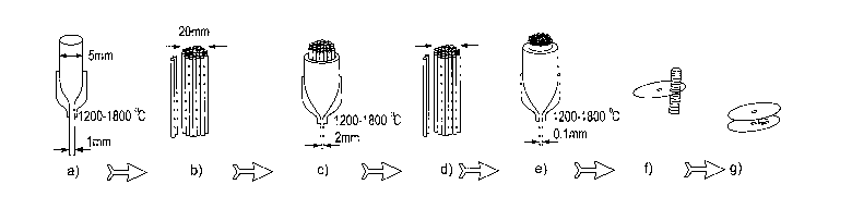
Figure 1 is a flow diagram showing the steps taken to fabricate a nanoscale
optical
device;
Figure 2 is a cross section through an optical device fabricated using the
technique
of Figure 1;
Figure 3 (a) is a simulation of the intensity distribution at the focal plane
for an
ideal 1 D parabolic gradient index lens with a diameter of 40 micrometers;
Figure 3(b) is a simulation of the cross-section of the focal spot at the
focal plane
for the lens of Figure 3(a);
Figure 4 (a) is a simulation intensity distribution at the focal plane for a
nanostructured microlens with a diameter of 40 micrometers;
Figure 4(b) is a simulation of the cross-section of the focal spot at the
focal plane
for the lens of Figure 4(a);
Figure 5(a) is a representation of an ideal 2D parabolic gradient lens with a
diameter of 10 micrometers;
Figure 5(b) is a representation of a nanostructured lens that has properties
designed to be the same as the lens of Figure 5(a);
Figure 6(a) shows a simulation of intensity distribution at the focal plane
for the
nanostructured microlens of Figure 5(b), and
Figure 6(b) shows a simulation of the cross-section of focal spot at the focal
plane
for the lens of Figure 5(b).
Detailed Description of the Drawings
The present invention is based on the well-established "stack and draw" method
of
fabrication, currently used in the creation of imaging plates and double-glass
photonic
crystals. This is illustrated in Figure 1. The stack and draw method has
previously only
CA 02658406 2009-01-16
WO 2008/009873 PCT/GB2007/002018
3
been used for drawing materials of the same composition. In contrast, in the
present
invention a plurality of different materials is used, so that composites can
be formed, and
devices made from such composites.
Fabrication commences with the assembly of a macroscopic preform with the same
structure and pattern as that desired in the final material. To make such a
macroscopic
preform, it is preferable to stack a large number of rods or fibers, for
example glass rods or
fibers, together in a desired structure and pattern, as illustrated in Figure
lb. These rods
may be manufactured using standard drawing technologies or any other suitable
technique. The rods or fibers should preferably be of similar diameter,
preferably around
1mm, and be thermally matched, so that their coefficient of thermal expansion,
softening
point and transition temperature should be close. When these conditions are
fulfilled the
end material will have minimal internal tension and, in the case where glass
rods are
utilized, similar mechanical properties to a monolithic slab of glass.
The bundled rods are heated to a temperature sufficient to soften and bind
them together
and allow their drawing into one single rod. Drawing can be done in any
suitable drawing
structure. Where glass fibers are used, this structure can be a fiber-drawing
tower. For
glass, the temperature of this tower should be in the region of 1200 to 1600
degrees
centigrade. After drawing, this drawn rod is allowed to set and is cut into a
number of
intermediate preforms. These intermediate preforms are then bundled together
to form the
final pattern, as illustrated in Figure 1 d. This bundle is processed to
generate the final
nanostructured preform, as illustrated in Figure le, by the application of
sufficient heat to
bind the preforms together followed by `drawing' of the material by pulling
the heated
preforms through the drawing structure. This final structured preform may have
nanometer feature sizes.
If necessary or desired the stack and draw steps can be repeated, or a number
of different
final nanostructured preforms can be combined in order to make an array of
structures
rather than a single structure. In this case, the final nanostructured preform
is cut a number
of times, or a number of differing final nanostructured performs are
fabricated, and the
resultant preforms bundled together, processed through the application of heat
and
drawing, as previously described, to give a single rod consisting of an array
of the
nanostructured preforms - a nanostructured preform array. In the case where
glass rods
CA 02658406 2009-01-16
WO 2008/009873 PCT/GB2007/002018
4
and a fiber drawing tower are used, the temperature of this fiber drawing
tower should be
in the region of 1200 to 1600 degrees centigrade.
Finally, the nanostructured preform or nanostructured preform array, generally
in the form
of a rod, is cut into pieces with a length according to the desired design
functionality, as
illustrated in Figure 1 f, to give the final nanostructured material. This
step is not necessary
in every case. If the nanostructured preform or nanostructured preform array
is already of
sufficient length, it may not require cutting, and can be considered the final
nanostructured
material without any further action. The material can then be polished if
required, as
illustrated in Figure 1 g. Again, this step is not necessary in every case,
only where the
ends of the final nanostructured material are of insufficient quality to allow
the entry and
exit of light, if they are to be used as light transmitting devices. For
example, if the cut
applied to the material is of high enough quality, there may not be any need
for polishing
at all.
To develop a new optical element using the technique in which the invention is
embodied,
the device properties desired firstly have to be modeled. This can be done,
for example,
by calculating a phase profile of the element, preferably a continuous phase
profile.
Having a continuous phase profile results in best quality output. This is
because it is
closer to the profile of a conventional device, such as a lens, rather than a
binary phase
structure. The phase difference can be more than 27C. Once the phase profile
is determined,
the distribution of nanosized elements in a 2D matrix is calculated. At this
stage the
optical properties of the volume dielectric materials are determined by
designing the final
required element and converting the required phase distribution to a
refractive index
distribution. This refractive index distribution can then be used as the basis
for
determining the position and distribution of the different materials of the
various preforms
that are to be used in the drawing process. Once the device is modeled, the
preform is
fabricated as described previously and used to make an intermediate preform.
Then the
intermediate preform is drawn and the nanostructured preform is formed. Then
the final
nanostructured preform is cut, bundled, heated and drawn and subsequently cut
into plates
with appropriate length for the nanostructured optical elements. If necessary
the cut
surface is polished to obtain optical quality.
CA 02658406 2009-01-16
WO 2008/009873 PCT/GB2007/002018
Figure 2 shows an example of a nanostructured lens fabricated in accordance
with the
present invention. As can be seen this has flat optical surfaces, and is
formed from a
plurality of materials that have a different refractive index. The materials
take the form of
columns that extend through and along the optical path of the entire device.
As noted
5 above, by appropriately designing and selecting the distribution of the
different materials,
any optical function can be provided. This has numerous advantages over the
prior art.
Having flat surfaces means that the device can be readily subjected to further
processing,
for example polishing or the application of a coating. Equally, in some
circumstances, no
further processing of the device is needed. This can be a significant
advantage over
conventional techniques for fabricating, for example, concave or convex
lenses, which
require careful shaping and polishing techniques to be used.
To compare the properties of a nanostructured microlens fabricated using the
present
invention to an `ideal' parabolic standard gradient index microlens, which has
a high
refractive index in the middle and a low refractive index nearer the edges, a
series of
Finite Difference Time Domain (FDTD) simulations were carried out. The results
of
these are shown in Figures 3 to 6.
In a first set of simulations, 1 D lenses with a diameter of 40 m, effective
focal length
f 66 m and f-number=l.5 were investigated. A wavelength of 2,=1550 nm with TM
polarization and a space discretization of 50 nm/cell (X/30) was assumed. The
results of a
simulation performed for a conventional, ideal parabolic gradient index lens
are illustrated
in Figure 3, where Figure 3 (a) is a simulation of the intensity distribution
at the focal
plane for a gradient index lens with a diameter of 40 micrometers and Figure
3(b) is a
simulation of the cross-section of the focal spot at the focal plane for the
lens of Figure
3(a). The results of the simulation performed for a nanostructured microlens
made in
accordance with the present invention using nanorods of only two types of
glass are
illustrated in Figure 4, where Figure 4 (a) is a simulation intensity
distribution at the focal
plane for a nanostructured microlens with a diameter of 40 micrometers and
Figure 4(b) is
a simulation of the cross-section of the focal spot at the focal plane for the
lens of Figure
4(a). From Figures 3 and 4, it can be seen that the characteristics of the
device made in
accordance with the invention compare very well with those of the conventional
lens.
CA 02658406 2009-01-16
WO 2008/009873 PCT/GB2007/002018
6
In another simulation, a flat plate nanostructured microlens, as shown in
Figure 5(b), was
simulated so as to have properties similar to that of an ideal 2D parabolic
gradient index
lens with a diameter of 10 m, as shown in Figure 5(a). The simulated
nanostructured
microlens was assumed to be fabricated in accordance with the invention from
two type of
rods with a refractive index of n=1.619 (F2 glass) and n=1.518 (NC21 glass)
respectively.
Figures 6(a) and (b) show the results of the simulation for the nanostructured
microlens.
This had a focal length of Lh_~155.75 m and the diameter of the beam at focus
was equal to
5 m - the same as in case of the parabolic gradient index lens. Both
microlenses have the
same value of effective focal length and diameter of the beam at the focus. In
addition, as
shown in Figure 6(b), the diameter of the focal spot for the nanostructured
microlens is
diffraction limited, as in case of ideal gradient index lens. Hence, these
simulations show
that using the present invention it is possible to obtain nanostructured
microlenses with
parameters similar to `ideal' gradient index microlenses.
The present invention provides numerous benefits. For example, it allows the
manufacture of optical devices having flat optical surfaces without any
curvature. This is
useful for microlenses and DOEs. In addition, devices can be easily integrated
in 2D
arrays with a filling factor close to 100%. Also arbitrary phase profiles can
be obtained.
This means that any desired device can be produced, for example lenses, in
particular
spherical lenses, aspherical lenses, elliptical lenses, cylindrical lenses,
axicon, and lenses
with or without double focus. Using the present invention, all of these can be
fabricated
with micro or nanoscale features. Also, every element of a 2D array of
elements could be
arranged to have individual features and phase properties. Also, by suitably
arranging the
different fibers or rods, a single device can be arranged to have several
different functions.
For example, one area could be designed as an ashperic micro-lens, whilst
another could
be an axicon. This facilitates the manufacture of fully integrated optical
systems in a
single flat plate device.
A skilled person will appreciate that variations of the disclosed arrangements
are possible
without departing from the invention. For example, whilst the invention has
been
described primarily with reference to drawing glass fibers, it will be
appreciated that other
materials could be used. Equally, each rod or fiber need not be made of a
single material,
but instead could, for example, comprise a core material, such as glass, and
be coated with
CA 02658406 2009-01-16
WO 2008/009873 PCT/GB2007/002018
7
another material. Accordingly the above description of the specific embodiment
is made
by way of example only and not for the purposes of limitation. It will be
clear to the
skilled person that minor modifications may be made without significant
changes to the
operation described.