Note: Descriptions are shown in the official language in which they were submitted.
CA 02658763 2009-01-22
WO 2008/013999
PCT/US2007/017019
1
TITLE
SYSTEM AND METHOD FOR FAST SIGNAL ACQUISITION
IN A WIRELESS DIGITAL RECEIVER FOR VVIDEBAND SIGNALS
INVENTOR
SASHCALA DIVAICARUNI
FIELD OF THE INVENTION
This invention addresses the need to transport high bit-rate data over wired
or
wireless means using specially modulated radio frequency carrier waves.
Specifically, a receiver synchronization technique is described in this
disclosure that
significantly reduces the convergence time for synchronization further
enabling
specially modulated radio frequency carrier waves.
BACKGROUND OF THE INVENTION
Modulation is the fundamental process in any communication system. It is a
process to impress a message (voice, image, data, etc.) on to a carrier wave
for
transmission. A band-limited range of frequencies that comprise the message
(baseband) is translated to a higher range of frequencies. The band-limited
message is
preserved, i.e., every frequency in that message is scaled by a constant
value, and then
transmitted by a transmitter. The three key parameters of a carrier wave are
its
amplitude, its phase and its frequency, all of which can be modified in
accordance
with an information signal to obtain the modulated signal. The receiver then
must
select the correct transmitted signal from all the signals being transmitted
by other
transmitters in the area, and demodulate the signal using the same parameters
the
baseband signal was modulated with.
There are various shapes and forms of modulators and demodulators. For
example conventional Amplitude Modulation uses a number of different
techniques
for modulating and demodulating the amplitude of the carrier in accordance
with the
CA 02658763 2009-01-22
WO 2008/013999
PCT/US2007/017019
2
information signal. These techniques have been described in detail in "Modern
Analog and Digital Communication Systems" by B.P. Lathi. Similarly
conventional
Frequency / Phase Modulation uses a number of different methods described in a
number of textbooks. In all these techniques, carrier (which is a high
frequency
sinusoidal signal) characteristics (either amplitude, frequency, phase or
combination
of these) are changed in accordance with the data (or information signal) by
the
modulator and changed back by the demodulator after transmission.
Conununication systems that have emerged in recent years include mono-
pulse and Ultra-Wide Band communication systems. The problem with these
systems
is that all mono-pulse or Ultra-Wide Band communications systems form Power
Spectrum Densities that tend to span very wide swaths of the radio spectrum.
For
instance the FCC has conditionally allowed limited power use of UWB from 3.2
GHz
to 10 GHz. These systems must make use of very wide sections of radio spectrum
because the transmit power in any narrow section of the spectrum is very low.
Generally any 4 KHz section of the affected spectrum will contain no more than
¨
42dbm of UWB spectral power. Correlating receivers are used to "gather" such
very
wide spectral power and concentrate it into detectable pulses. Interfering
signals are
problematic. Since the communication system is receiving energy over a very
wide
spectrum, any interfering signal in that spectrum must be tolerated and
mitigated
within the receiver. Many schemes exist to mitigate the interference. Some of
these
include selective blocking of certain sections of spectrum so as not to hear
the
interferer, OFDM schemes that send redundant copies of the information in the
hope
that at least one copy will get through interference, and other more exotic
schemes
that require sophisticated DSP algorithms to perform advanced filtering. In
addition,
UWB systems have somewhat of a "bad reputation" because they at least have the
potential to cause interference. A heated discourse has gone on for years over
the
potential that UWB systems can cause interference to legacy spectrum users.
Tri-State Integer Cycle Modulation (TICM) and other = Integer Cycle
Modulation techniques were invented by Joe Bobier to help alleviate this
massive and
CA 02658763 2009-01-22
WO 2008/013999
PCT/US2007/017019
3
growing problem which has now become known by its commercial designation, xG
Flash Signaling. Its signal characteristics are such that absolute minbnal
sideband
energy is generated during modulation but that its power spectrum density is
quite
wide relative to the information rate applied. Also, a narrower section of the
power
spectrum output can be used to represent the same information. The technique
of
receiver synchronization disclosed herein is primarily applicable to these
types of
single cycle systems and Ultra Wide Band systems.
In a wireless network using TDMA for multiple access, each user is assigned a
time slot for transmission and reception. The receiver in these systems has to
acquire
and maintain precise synchronization with the transmitter in order to
accurately
extract the payload data from the received data. The receiver needs to
determine
symbol timing, carrier frequency offset, and carrier phase offset. The
synchronization
subsystem in the receiver determines these factors for each received burst of
data.
The synchronization subsystem has severe performance constraints in terms of
processing time. This in turn places heavy demands on DSP performance and the
digital acquisition and data .transfer system itself. The amount of time this
search
takes directly relates to the time slot requirements and the throughput of the
receiver.
A traditional TDMA receiver will start sampling data when in its intended
timeslot. An entire timeslot's worth of data is presented to the DSP. Every
burst of
data contains a known sequence of bits that precede the payload data, called
the
preamble. The synchronization subsystem will start searching for the preamble
starting from the very first sample it received. Various methods are used to
determine
the location of the preamble, such as correlation, MLSE, etc.
The time it takes to process and search through all the samples from the start
of the timeslot to the start of the preamble can be called convergence time.
The time
taken by the digital acquisition system to transfer an entire timeslot's worth
of data
can be called data transfer time.
CA 02658763 2009-01-22
WO 2008/013999
PCT/US2007/017019
4
The disclosure of this application provides a method, called Symbol Sensed
Synchronization (SSS), that significantly reduces the convergence time for
synchronization. This method also significantly reduces the transfer time, and
the
memory required for data storage.
BRIEF SUMMARY OF THE INVENTION
This invention addresses the need to transport high bit-rate data over wired
or
wireless means using specially modulated radio frequency carrier waves.
Specifically, a receiver synchronization technique is described in this
disclosure that
significantly reduces the convergence time for synchronization further
enabling
specially modulated radio frequency carrier waves.
In general this method achieves fast synchronization using the following
steps:
the characteristics of the baseband signal are used to detect the start of the
received
burst. Once the presence of a symbol is detected, the data acquisition
subsystem is
enabled to begin collecting samples. These samples are then transferred to the
DSP.
The DSP then searches for a preamble to precisely determine the timing delay
to the
start of the payload data.
For a fuller understanding of the nature and objects of the invention,
reference
should be made to the following detailed description taken in connection with
the
accompanying drawings.
DESCRIPTION OF THE DRAWINGS
For a fuller understanding of the nature and objects of the invention,
reference
should be made to the accompanying drawings, in which:
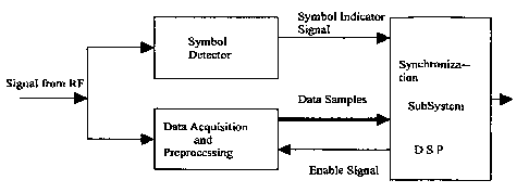
FIGURE 1 is a block diagram of a receiver subsystem;
FIGURE 2 is a representation of a sequence of events in a receiver timeslot;
FIGURE 3(a) is a representation of the symbol detector subsystem;
FIGURE 3(b) is a representation of the RF signal input to the symbol detector
CA 02658763 2009-01-22
WO 2008/013999
PCT/US2007/017019
subsystem;
FIGURE 3(c) is a representation of the output of the symbol detector
subsystem;
FIGURE 4 is a flowchart of a software design to implement the symbol sensed
synchronization.
DETAILED DESCRIPTION OF THE INVENTION
As discussed above this invention addresses the need to transport high bit-
rate
data over wired or wireless means using specially modulated radio frequency
carrier
waves. More specifically, a receiver synchronization technique is described
that
significantly reduces the convergence time for synchronization further
enabling
specially modulated radio frequency carrier waves.
The system and method of this disclosure achieves fast synchronization using
the following steps: the characteristics of the baseband signal are used to
detect the
start of the received burst. Once the presence of a symbol is detected, the
data
acquisition subsystem is enabled to begin collecting samples. These samples
are then
transferred to the DSP. The DSP then searches for a preamble to precisely
determine
the timing delay to the start of the payload data.
The block diagram of the receiver that implements the Symbol Sensed
Synchronization is given below in Figure 1. In Figure 2, the sequence of
events in one
timeslot is shown. The receiver is designed for the xG Flash Signaling
modulation and
coding technology as described above.
At the start of the receiver's timeslot, denoted by time X in Fig 2, the
signal at
the receiver front end is sampled at the sampling frequency. This signal is
fed into the
Symbol Detector, which then provides a threshold limited signal to the DSP for
each
sample starting from time X. The actual transmitted burst is not received
until time Y
in the timeslot. The signal level of each sample denotes the presence or
absence of a
data symbol.
CA 02658763 2009-01-22
WO 2008/013999
PCT/US2007/017019
6
The DSP will monitor this signal for a change in signal level. Once the DSP
detects this change, it will enable the data acquisition subsystem to start
data pre-
processing, and data transfer to the DSP. The acquisition and pre-processing
subsystem now "wakes up" after time A, at time Y in Fig 2. The incoming data
samples from the RF front end are now processed, and the transfer to the DSP
is
started.
The maximum burst size is known to the DSP. This size is denoted by time B
in Fig 2. The DSP will disable the data acquisition system once it has
received all
samples for the maximum burst size.
Once all the data is available, the DSP will search for the preamble and
determine the timing delay. From here on, it continues with the required
processing,
such as determining the frequency offset, phase offset, etc.
The major advantages of Symbol Sensed Synchronization are as follows:
I) Reduction in the amount of time taken to transfer received burst data from
an
entire timeslot's worth to the maximum transmitted burst size.
2) Reduction in the amount of memory required for storage of the received
burst
data, which in turn reduces the cost of the system.
3) Fast synchroni7ation time due to the fact that the preamble search begins
at the
start of the transmitted burst, and not at the start of the timeslot.
4) Rediiced probability of false preamble detection.
5) Higher data throughput rates from the receiver due to fast synchronization
times.
6) Although this method can be used in full duplex and half duplex systems, it
is
especially useful for one way broadcast transmission systems.
7) Short preambles can be used, increasing the amount of payload data
transmitted in one burst.
CA 02658763 2015-03-09
7
A more complete description of the preferred embodiment of the individual
blocks shown
in Figure 1 is given below.
Symbol Detector Subsystem. This subsystem is a comparator as further shown in
figure
3(a). The input to this subsystem is the signal from the RF front-end section
of the receiver
shown in figure 3(b). The input is fed into a comparator, which compares this
to a
threshold setting. Any value of the signal above the threshold results in a
logic level 1 at
the output of the comparator as shown in figure 3(c). Otherwise the comparator
output is at
logic level O. The output of the comparator is tied to a general purpose 10
pin of the DSP.
Data Acquisition and Pre-processing subsystem. The input to this subsystem is
the
baseband signal from the RF front-end. This subsystem is in sleep mode until
the "enable"
signal is provided from the DSP. Once enabled, the input signal is processed
and converted
to a format acceptable by the DSP. This sampled data is fed into the DSP via a
transfer
interface. The process of acquisition, preprocessing and transfer continues
until a "disable"
signal is received from the DSP. This subsystem is easily implemented by one
skilled in
the art
Software Design. The software required to implement the SSS method is
illustrated in the
flowchart shown in figure 4 which can be easily implemented in code by someone
skilled
in the art.
The scope of the claims should not be limited by the preferred embodiments set
forth in the
examples, but should be given the broadest interpretation consistent with the
description as a
whole.