Note: Descriptions are shown in the official language in which they were submitted.
CA 02660402 2009-02-09
WO 2008/024206 PCT/US2007/017666
TITLE OF THE INVENTION
FRONT CONTACT WITH INTERMEDIATE LAYER(S) ADJACENT
THERETO FOR USE IN PHOTOVOLTAIC DEVICE AND METHOD OF
MAKING SAME
[0001] This invention relates to a photovoltaic device including a front
contact. In certain example embodiments, the front contact of the photovoltaic
device
includes a glass substrate that supports a transparent conductive oxide (TCO)
of a
material such as tin oxide, zinc oxide, or the like: An intermediate film is
provided
between the TCO of the front contact and an absorbing semiconductor film of
the
photovoltaic device. The intermediate film is designed so as to improve
operation
efficiency of the photovoltaic device in certain example instances.
BACKGROUND AND SUMMARY OF EXAMPLE EMBODIMENTS OF
INVENTION
[0002] Photovoltaic devices are known in the art (e.g., see U.S. Patent Nos.
6,784,361, 6,288,325, 6,613,603, and 6,123,824, the disclosures of which are
hereby
incorporated herein by reference). Amorphous silicon photovoltaic devices, for
example, include a front contact or electrode. Typically, the transparent
front contact
is made of a transparent conductive oxide (TCO) such as zinc oxide or tin
oxide (e.g.,
Sn02:F) formed on a substrate such as a glass substrate. In many instances,
the
transparent front contact is formed of a single layer using a method of
chemical
pyrolysis where precursors are sprayed onto the glass substrate at
approximately 400
to 600 degrees C. The front contact is typically positioned directly on and
contacting
an absorbing semiconductor film/layer (including one or more layers) of the
device.
[0003] Unfortunately, convention photovoltaic devices often reflect
significant amounts of incident radiation before such radiation can be
converted into
electrical energy by the device, thereby leading to inefficient operations.
[0004] Thus, it will be appreciated that there exists a need in the art for a
photovoltaic device capable of operating =in a more efficient manner.
1
CA 02660402 2009-02-09
WO 2008/024206 PCT/US2007/017666
[0005] In certain example embodiments of this invention, an intermediate film
including at least one layer is provided between the front contact and an
absorbing
semiconductor film (absorber) of the photovoltaic. device. The intermediate
film may
be discrete or refractive index graded, continuously or discontinuously, in
certain
example embodiments of this invention. The refractive index (n) of the
intermediate
film is tuned or designed so as to satisfy one or more of the following: (a)
reduce
optical reflection of solar radiation from the TCO/absorber interface thereby=
enhancing the amount of radiation which penetrates the absorber and which can -
be
converted into electrical energy so as to iniprove 'efficiency of the device,
(b) increase
the amount of radiation trapped within the absorber which can be converted
into
electrical energy, (c) reduce cross-diffusion of elements between the TCO of
the front
contact and the absorbing semiconductor film, and/or (d) form a high
resistivity
buffer layer (HRBL) between the front contact TCO and the absorber film.
[0006) In certain example embodiments of this invention, the intermediate
film may be made of or include a semiconductor material. Being an integrated
part of
the layer stack of the photovoltaic device, the intermediate film may be a
robust anti-
reflection (AR) film with additional po'ssible barrier properties.
[0007] In certain example embodiments of this invention, there is provided a
photovoltaic device comprising: a front glass substrate; a semiconductor film
including p-type, n-type and i-type layers; a substantially transparent
conductive
oxide (TCO) based film located between at least the front glass substrate and
the
semiconductor film; and an intermediate film located between the TCO based
film
and the semiconductor,film, wherein the intermediate film has a refractive
index (n)
that is higher than that of the TCO based film and lower than that of the
semiconductor film.
100081 In other example embodiments of this invention, there is provided a
photovoltaic device comprising: a front glass substrate; a semiconductor
absorber
film; a substantially transparent conductive oxide (TCO) based fifm located
between
-at least the front glass substrate and the semiconductor absorber film; and
an
intermediate film located between the TCO based film and the semiconductor
absorber film, wherein the intermediate film has a refractive index (n) of
from about
2
CA 02660402 2009-02-09
WO 2008/024206 PCT/US2007/017666
2.0 to 4.0 and which is higher than that of the TCO based film and lower than
that of
the semiconductor absorber film.
[0009] In still further example embodiments of this invention, there is
provided a method of making a photovoltaic device, the method comprising:
providing a substrate; depositing a first substantially transparent conductive-
oxide
(TCO) film on the substrate; forming an intermediate film on the substrate
over at
least the TCO film, wherein the intermediate film has a refractive index (n)
of from
about 2.0 to 4.0 and which is higher than that of the TCO film; and forming
the
photovoltaic device so that the intermediate film is located between the TCO
film and
a semiconductor film of the photovoltaic device.
BRIEF DESCRIPTION OF THE DRAWINGS
[0010] FIGURE 1 is a cross sectional view of an example photovoltaic device
according to an example embodiment of this invention.
[0011]. FIGURES 2(a), 2(b) and 2(c) are schematic diagrams illustrating
improved optical results associated with the intermediate film in certain
example
embodiments of this invention.
100121 FIGURE 3 is a graph illustrating the ratio (G) of the amount of light
trapped within the absorbing semiconductor film in a photovoltaic device
having an
intermediate film according to examples of this invention compared to a device
'
without the intermediate film.
[0013] FIGURE 4 is a graph illustrating results of using a bi-layer
intermediate film according to examples of this invention.
DETAILED DESCRIPTION OF EXAMPLE EMBODIMENTS OF THE INVENTION
[0014] Photovoltaic devices such as solar cells convert solar radiation and
other light into usable electrical energy. The energy conversion occurs
typically as
3
CA 02660402 2009-02-09
WO 2008/024206 PCT/US2007/017666
the result of the photovoltaic effect. Solar radiation (e.g., sunlight)
impinging on a
photovoltaic device and absorbed by an active region of semiconductor material
(e.g.,
a semiconductor film including one or more semiconductor layers such as a-Si
layers)
generates electron-hole pairs in the active region. The electrons and holes
may be
separated by an electric field of a junction in the phofovoltaic device. The
separation
of the electrons and holes by the junction results in the generation of an
electric
current and voltage. In certain example embodiments, the electrons flow toward
the
region of the semiconductor=material having n-type conductivity, and holes
flow =
toward the region of the semiconductor having p-type conductivity. =Current
can flow
through an external circuit connecting the n-type region to the p-type region
as light
continues to generate electron-hole pairs in the photovoltaic device.
[0015] In certain example embodiments, single junction amorphous silicon (a- =
Si) photovoltaic devices include at least three semiconductor layers making up
an
absorbing semiconductor film. In particular, a p-layer, an n-layer and an i-
layer
which is intrinsic can make up the absorbing semiconductor film in certain
example
instances. The amorphous silicon film (which=may include one or more layers
such as
p, n and i-type layers) may be of hydrogenated amorphous silicon in certain
instances,
but may also be of or include hydrogenated amorphous silicon carbon or
hydrogenated amorphous silicon germanium, or the like, in certain example
embodiments of this invention. For example and without limitation, when a
photon of
light is absorbed in the i-layer it gives rise to a unit of electrical current
(an electron-
hole pair). The p and n-layers, which contain charged 'dopant ions, set up an
electric
field across the i-layer which draws the electric charge out of the i-layer
and sends it
to an optional external circuit where it can provide power for electrical
components.
It is noted that while certain example embodiments of this invention are
directed
toward amorphous-silicon based photovoltaic devices, this invention is not so
limited
and may be used in conjunction with other types of photovoltaic devices in
certain
instances including but not limited to devices including other types of
semiconductor
material, tandem thin-film solar cells, CdS/CdTe based solar cells, and the
like.
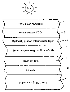
[0016] Fig. I is a cross sectional view of a photovoltaic device according to
an
example embodiment of this invention. The photovoltaic device includes
transparent
4
CA 02660402 2009-02-09
WO 2008/024206 PCT/US2007/017666
front glass substrate 1, front electrode or contact 3 which is of or includes
a
transparent conductive oxide (TCO) layer 3 such as tin oxide, fluorine-doped
tin
oxide, zinc oxide, aluminum-doped zinc oxide, indium tin oxide, indium zinc
oxide,
or the like, intermediate film 4, absorbing semiconductor film 5 of one or
more
semiconductor layers (e.g., including at least three layers of p, i, and n
types), back
electrode or contact 7 which may be of a TCO or a metal, an optional
encapsulant 9 or
adhesive of a material such as ethyl vinyl acetate (EVA) or the like, and an
optional
superstrate 11 of a material such as glass. Of course, other layer(s) which
are not
shown may also be provided in the device. Front glass substrate I and/or rear
superstrate (substrate) 11 may be made of soda-lime-silica based glass in
certain
example embodiments of this invention. While substrates 1, 11 may be of glass
in
certain example embodiments of this invention, other materials such as quartz
or the
like may instead be used. Moreover, superstrate 11 is optional in certain
instances.
Glass I and/or 11 may o` may not be thermally tempered and/or patterned in-
certain
example embodiments of this invention. Additionally, it will be appreciated
that the
word "on" as used herein covers both a layer/film being directly on and
indirectly on
something, with other layers possibly being located therebetween.
[0017] In certain example embodiments of this invention, the photovoltaic
device may be made by providing glass substrate 1, and then depositing (e.g.,
via
sputtering or any other suitable technique) TCO 3 on the substrate 1. Then,
the
intermediate layer 4 is deposited on the substrate 1 over and contacting the
TCO 3.
Thereafter the structure including substrate 1, front contact 3, and
intermediate layer 4
may be coupled with the rest of the device in order to form the photovoltaic
device
shown in Fig. 1. For example, the semiconductor layer 5 may then be formed
over
the front contact structure on substrate. 1, or alternatively may be formed on
the other
substrate with the front contact structure thereafter being cbupled to the
same. Front
contact layer 3 and intermediate film 4 are typically continuously, or
substantially
continuously, provided over substantially the entire surface of the
semiconductor film,
in certain example embodiments of this invention. In certain example
embodiments
of this invention, the front contact 3 may have a sheet resistance (RS) of
from about 7-
50 ohms/square, more preferably from about 10-25 ohms/square, and most
preferably
5
CA 02660402 2009-02-09
WO 2008/024206 PCT/US2007/017666
from about 10- 15 ohms/square using a reference example non-limiting overall
thickness of from about 1,000 to 2,000 angstroms.
[0018] The absorbing or active semiconductor region or film 5 may include
one or more layers, and may be of any suitable material. For example, the
absorber
semiconductor film 5 of oine type of single junction amorphous silicon (a-Si)
photovoltaic device includes three semiconductor layers, namely a p-layer, an
n-layer
and an i-layer. The p-type a-Si layer of the semiconductor film 5 may be the
uppermost portion of the semiconductor film 5 in certain example=embodiments
of
this invention; and= the i-layer is typically located between the p and n-type
layers.
These amorphous silicon based layers of film 5 may be of hydrogenated
amorphous
silicon in certain instances, but may also be of or include hydrogenated
amorphous
silicon carbon or hydrogenated amorphous silicon germanium, or other suitable
=material(s) in certain example embodiments of this invention. It is possible
for the
semiconductor region 5 to be of a double-junction type in alternative
embodiments of
this invention.
[0019] Back contact or electrode 7 maybe of any suitable electrically
conductive material. For example and without limitation, the back contact or
electrode 7 may be of a TCO and/or a metal in certain instances. Example TCO
materials for use as back contact or electrode 7 include indium zinc oxide,
indium-tin-
oxide (ITO), tin oxide, and/or zinc oxide which may be doped with aluminum
(which
may or may not be doped with silver). The TCO of the back contact 7 may be of
the
single layer type or a multi-layer type in different instances. Moreover, the
back
contact 7 may include both a TCO portion and a metal portion in certain
instances.
For example, in an example multi-layer embodiment, the TCO portion of the back
contact 7 may include a layer of a material such as indium zinc oxide (which
may or
may not be doped with silver), indium-tin-oxide (ITO), tin oxide, and/or zinc
oxide
.closest to the active region 5, and the back contact may include another
conductive
and possibly reflective layer of a material such as silver, molybdenum,
platinum,
steel, iron,= niobium, titanium, chromium, bismuth, antimony, or aluminum
further
from the active region 5 and closer to the superstrate 11. The metal portion
may be
closer to superstrate 11 compared to the TCO portion of the back contact 7.
6
CA 02660402 2009-02-09
WO 2008/024206 PCT/US2007/017666
[0020] The photovoltaic module may be encapsulated or partially covered
with an encapsulating material such as encapsulant 9 in certain example
embodiments. An example encapsulant or adhesive for layer 9 is EVA. However,
other materials such as Tedlar type plastic, Nuvasil type plastic, Tefzel type-
plastic or
the like may instead be used for layer 9 in different instances.
[0021] Intermediate film 4 including at least one layer is provided between
the
front contact 3 and absorbing semiconductor film (absorber) 5 of the
photovoltaic
device. The intermediate film 4 may be discrete or refractive index graded, _
continuously or discontinuously, in certain example embodiments of this
invention.
The refractive index (n) of the intermediate film 4 is tuned or designed so as
to satisfy
one or more of the following: (a) reduce optical reflection of solar radiation
due to
the TCO/absorber interface (i.e., interface between films 4 and 5) thereby
enhancing
the amount of radiation which penetrates the absorber and which can be
converted
into electrical energy so as to improve efficiency of the device, (b) increase
the
amount-of radiation trapped within the absorber 5 whicli can be converted into
electrical energy, (c) reduce cross-diffusion of elements between the TCO 3 of
the
front contact and the absorbing semiconductor film 5 (e.g., to reduce cross
diffusion
of oxygen and hydrogen between films 3 and 5 in the example case where zinc
oxide
is used as the TCO 3 and a-Si:H is used in the absorber film 5), and/or (d)
forrn a high
resistivity buffer layer (HRBL) in certain cases (e.g.; in a CdS/CdTe based
solar cell)
between the front contact TCO 3 and the absorber film 5 in order to improve
device
performance.
[0022) In certain example embodiments of this invention, the intermediate
film 4 may be made of or include a semiconductor material, including but not
limited
to one or more of Nb-doped anatase TiO,, TiO,, or the like. In certain example
embodiments of this invention, the intermediate film is designed so that all
or a
portion thereof has a refractive index (n) of from about 2.0 to 4.0, more
preferably
from about 2.1 to 3.2, and most preferably from about 2.15 to 2.75 (e.g., Nb-
doped
anatase TiOX can be formed so as to have a refractive index n of about 2.4).
The
intermediate film 4 may or may not be index (n) graded in certain example
embodiments of this invention. For instance, when not graded the entire
thickness of
7
CA 02660402 2009-02-09
WO 2008/024206 PCT/US2007/017666
film 4 has an approximately constant refractive index (n) and an approximately
constant chemical make-up through its' thickness. However, when graded, the
film 4
may be graded in a manner so that its refractive index (n) and/or material
make-up
changes continuously or discontinuously throughout the film's thickness. For
example, in certain example embodiments the film 4 may comprise Nb-doped
anatase
TiO,,, where the film 4 is Nb-doped at an area in the film 4 adjacent the TCO
3 but is
either not doped or slightly doped at an area in the film 4 adjacent the
semiconductor
absorber 5, and the refractive index (n) and/or Nb content may vary
continuously or
discontinuously through the film's thickness or a portion thereof. As another
example, the intermediate film 4 may be index-graded by causing it to a higher
oxygen content (and thus a=lower refracti=ve index) at a portion therein
closer to the
TCO 3, and a lower oxygen content (and thus a higher refractive index) at a
portion
thereof farther from the TCO 3 and closer to the absorber 5; again, this
oxidation
= grading may be either continuous or discontinuous in different examples of
this
invention. Being an integrated part of the layer stack of the photovoltaic
device, the
intermediate film 4 may be a robust anti-reflection (AR) film with additional
possible
barrier properties such as reduction in diffusion and the like. In certain
example
embodiments of this invention, the Nb-doped TiO,, may include from about 0.1
to
25% Nb, more preferably from about 0.5 to 15% Nb, and most preferably from
about
1-10% Nb.
[00231 As mentioned above, the refractive index (n) of the intermediate film 4
can be tuned or designed so as to reduce optical reflection of solar radiation
due to the
TCO/absorber interface (i.e., interface between films 4 and 5) thereby
enhancing the
amount of radiation which penetrates the absorber and which can be converted
into
electrical energy so as to improve efficiency of the device. Disregarding film
4, there
may be a high refractive index (n) mismatch between the TCO 3 and the absorber
5;
this results in-a high amount of solar radiation reflection from the
TCO/absorber
interface which in turn causes reduced device efficiency. The introduction of
a
discrete (non-graded) or graded intermediate film 4 with a tuned refractive
index (n)
that is higher than that of the TCO 3 and lower than that of the semiconductor
absorber 5 reduces the amount of radiation (e.g., light) that is reflected and
thus acts
as an intemal anti-reflective (AR) filter. For purposes of example and
understanding,
8
CA 02660402 2009-02-09
WO 2008/024206 PCT/US2007/017666
the refractive indices of ZnAlOx (an example of TCO 3) and a-Si:H (an example
of
absorber semiconductor 5) for solar wavelengths are about 1.9 (ni) and 4.0
(n2),
respectively. Referring to Fig. 2(a), without intermediate film 4, this gives
the
amount of transmitted light reaching the absorber 5 from the TCO as in
equation (1)
below (note that Eo is the amplitude of light impinging on the TCO/absorber
interface
from the glass I side):
I12 = (Eotl2)2 ==[Eo (4ntn2/(nl+n2)2)]2 = [Eo (4x1.9x4.0/(1.9+4.0)2)12 =
0.7627Eo2 (1)
=[00241 However, the incorporation of discrete intermediate film 4 with an
example refractive index (n) of 2.4 results in the following increased amount
of light
reaching the absorber 5 as shown below in equation (2), referring to Fig.
2(b):
112 = (Eoti3t23)2 = [Eo (4nI n3/(nI +n3)2) (4n2n3/(n2+n3)2)]2
[Eo (4x1.9x2.4/(1.9+2.4)2) (4x4.0x2.4/(4.0+2.4)2)]2 = 0:8553Eo2 (2)
[0025] It will be appreciated that the increased amount of light reachirig the
absorber 5 (i.e., 0.8553Eo2) when intermediate film 4 is used (compared to
only
0.7627EQ2 when film 4 is not present) evidences about a 12% increase in
efficiency
and thus a significantly more efficient photovoltaic device. Referring to Fig.
2(c),
when the intermediate film 4 includes two layers 4a and 4b, efficiency can
also be
increased.
[0026] As a second possible advantage associated with certain example
embodiments of this invention, the refractive index (n) of the inten-nediate
film 4 can
be tuned or designed so as to increase the amount of radiation trapped within
the
semiconductor absorber 5 which can be converted into electrical energy,
thereby
improving efficiency of the photovoltaic device. In certain example
embodiments,
the provision of intermediate film 4 results in a redistribution of the
intensity of solar
radiation (e.g., light) reflected from the TCO/absorber interface toward the
front of
the photovoltaic device and the intensity of radiation (e.g., light) trapped
within the
semiconductor absorber film 5. The fornmer can play a role in determining the
amount
of radiation reaching the absorber, while the latter can play a role in
determining the
amount of radiation participating in multiple reflections within the absorber
5 and thus
dictating the efficiency of the device. This portion of radiation also has a
probability
9
CA 02660402 2009-02-09
WO 2008/024206 PCT/US2007/017666
to generate charge carriers. Generally speaking, the amplitude of solar light
penetrating from the TCO 3 into the absorber 5 may be said to be,
Ein = t12E0 (3)
[0027] Taking into account the first and second order reflections from the
back electrode 7 and the TCO 3/absorber 5 interface (see Fig. 2a), the
amplitude=of
light within the absorber may be said to be:
Eiõ = t12 Eo (1 + R + r12R + r12R2) = ti 2 Efl (1 + R)(1 + rlzR) (4)
which gives the light intensity
Iin = t122E02 (1+R)2 (1+ r12R)Z (5)
[00281 When the intermediate film 4 is incorporated as shown in Fig. 2(b), the
light intensity within the absorber becomes
lin = t122 t232E02 (1+R)2 (1+ r23R)2 (6)
[0029] Thin film photovoltaic devices such as solar cells typically exhibit
rather low conversion efficiency due to a small absorption coefficient of the
absorber
5; therefore, a reflective metal back contact 7 has often been used. Most
metals used
for back reflectors (e.g., Cr and Mo) reflect no more than about 25% of light
at solar -
wavelengths of 600-700 nm. An Al back contact in a-Si:H solar cells may
reflect
about 75%, but can lead to degradation of the device.
[0030] Fig. 3 demonstrates the ratio (G) of the amount of light trapped within
the absorber 5 in the device with the intermediate film 4, compared to the
device
without the intermediate film 4. It is noteworthy that G increases when a less
efficient
back reflector is used. About 10% of light intensity can be achieved. At the
same
time, the maximum of G shifts toward higher values of refractive index (n) of
the
intermediate film 4. As the index (n) of the intermediate film 4 reaches about
2.0 and
above, it can be seen that the ratio G advantageously increases thereby
illustrating an
increase in the amount of radiation trapped within the semiconductor absorber
5
which can be converted into electrical energy, thereby improving efficiency of
the
photovoltaic device. Moreover, because G increases when less efficient back
reflectors (e.g., see 0.2 and 0.4 in Fig. 3), it is possible to realize an
efficient
CA 02660402 2009-02-09
WO 2008/024206 PCT/US2007/017666
photovoltaic device while either not using a back reflector or while using a
less
efficient but possibly more desirable back reflector of a material such as Cr
and/or
Mo.
[00311 Fig. 4 is an example simulation of the results of optimization of a two-
layer intermediate film 4 at the TCO/a-Si:H interface. It has been found that
the
optimal combination for the bi-layer intermediate film 4 for an example TCO/a-
Si:H
interface is for a first layer 4b having a refractive index (n) of from about
2.25 to 2.6,
more preferably from about 2.3 to 2.55, with an example being about 2.4, and
the
second layer 4a having a lower refractive index of from about 2.0 to 2.25,
more
preferably from about 2.0 to 2.2, with an example being about 2.2. Note that
second
layer 4a with the. lower, refractive index is adjacent the TCO, and the layer
4b with the
higher refractive index is adjacent and contacting the absorber 5.
Additionally, index
grading of the film 4 from the lower-index material (see TCO 3) to the higher-
index
material (see absorber 5) can further increase the amount of light trapped in
absorber
which is advantageous.
[0032] Intermediate film 4 can also be advantageously used to reduce cross-
diffusion of elements between the TCO 3 of the front contact and the absorbing
semiconductor film 5 (e.g., to reduce cross diffusion of oxygen and hydrogen
between films 3 and 5 in the example case where zinc oxide is used as the TCO
3 and
a-Si:H is used in the absorber film 5). Certain types of solar cells (e.g., a-
Si:H solar
cells) use Sn02:F as a front transparent electrode or TCO 3. The use of tin
oxide can
lead to its darkening due to reduction in hydrogen atmosphere during the
absorber
deposition. Vacuum deposited ZnO doped with Group III elements is considered
as a
good a-Si:H TCO 3 candidate because of its resistance to hydrogen plasma
reduction.
There are other reasons, however, to avoid the exposure of ZnO to hydrogen
during
the a-Si:H deposition as well as to prevent the cross-diffusion of hydrogen
and
oxygen between the TCO and a-Si:H layers. The level of cross-diffusion is
determined by the difference in chemical potentials between the two layers, or
in
other words, by the amount the energy of the system would change when an
additional particle is introduced at the fixed entropy and volume. Hydrogen
causes
large lattice relaxation when introduced into ZnO, which is partially
responsible for
11
CA 02660402 2009-02-09
WO 2008/024206 PCT/US2007/017666
its rapid penetration in this material. At the same time, hydrogen is known to
have
very low activation energy of 0.17 eV in ZnO, which makes it diffusible in
ZnO.
Hydrogen forms unstable dorior-like 0-H complexes in ZnO, which eventually
form
H2 molecules, speculatively responsible for a drift in the device
characteristics over time. On the other hand, hydrogen facilitates oxygen
diffusion in the'a-Si:H layer.
This occurs according -to a two-step mechanism; in the first step hydrogen
opens up a
Si-Si bond for oxygen atom, and in the second step it saturates a Si broken
bond, thus
decreasing the activation energy of oxygen diffixsion. Cross-diffusion of
hydrogen
'and oxygen cause band bending at the TCO/a-Si:H interface and, as a result,
the
formation of an additional potential barrier, which in turn reduces the device
efficiency. The incorporation of the intermediate film 4 reduces cross-
diffusion of
atoms and ions between the TCO 3 and the absorber 5. Moreover, the use of
intermediate film 4 also permits zinc oxide and/or tin oxide to be used as the
TCO 3
without significantly suffering from the problems discussed above.
[0033] For purposes of example, in certain example embodiments of this
invention, intermediate film 4 can be produced by incorporating a discrete
TiNbOx
transparent conducting film between a ZnO TCO 3 and an a-Si:H absorber 5. An
example advantage of TiNbOx for film 4 is its high enthalpy of formation of
about
940 kJ/mol, which makes it more stable in sense of oxygen release compared to
ZnO
(350 kJ/mol) or Sn02(581 kJ/mol), thereby permitting it to reduce diffusion as
discussed above. Also, TiNbOx can have a desirable refractive index of from
about
2.1 to 3.2, more preferably frorn about 2.15 to 2.75, with an example index
(n) being
about 2.4.
[0034] . In certain example embodiments of this.invention, intermediate film 4
may be designed so as to form a high resistivity buffer layer (HRBL) (e.g., in
a
CdS/CdTe based solar cell) between the front contact TCO 3 and the absorber
film 5
in order to improve device performance. In certain example situations,
the.presence
of a HRBL between the TCO 3 and the abs6rber 5 (e.g., CdS/CdTe absorber) may
be
.desirable so as to enhance device performance and to provide at least some
protection
from shunting if there were to be pinholes in the CdS layer for example. In
such
cases, intermediate film 4, for example and without limitation, may be made of
or
12
CA 02660402 2009-02-09
WO 2008/024206 PCT/US2007/017666
include TiNbOx where the Nb dopant is either reduce or eliminated from the
film 4 at
or near the interface with the absorber. Other combinations of transparent
conductive
intermediate films 4 may also be used in different example embodiments of this
.invention.
[0035] While TiNbOx is mentioned above as a possible material for
intermediate film 4, this invention is not so limited. Other materials may
instead be
used for film 4, so long as one, two, three or four of-the aforesaid features
(a) through
(d) may be met. l;n particular, any suitable material of an appropriate
refractive index
or indices may be used for form film 4, so long as it is capable of resulting
in one or
more of the following: (a) reduce optical reflection of solar radiation due to
the
TCO/absorber interface (i.e., 'interface between films 4 and 5) thereby
enhancing the
amount of radiation which penetrates the absorber and which can be converted
into
electrical energy so as to improve efficiency of the device, (b) increase the
amount of
radiation trapped within the absorber 5 which can be converted into electrical
energy,
(c) reduce cross-diffusion of elements between the TCO 3 of the front contact
and the
absorbing semiconductor film 5, and/or (d) form a high resistivity buffer
layer
(HRBL) in certain cases between the front contact TCO 3 and the absorber film
5 in
order to improve device performance.
[0036] While the invention has been described in connection with what is
presently considered to be the most practical and preferred embodiment, it is
to be
understood that the invention is not to be limited to the disclosed
embodiment, but on
the contrary, is interided to cover various modifications and equivalent
arrangements
included within the spirit and scope of the appended claims.
13