Note: Descriptions are shown in the official language in which they were submitted.
CA 02660573 2009-02-11
WO 2008/021508 PCT/US2007/018286
INJECTION MOLDING OF CERAIVIIC ELEMENTS
The present application claims the benefit of U.S. application number
60/838,652 filed August 16, 2006, which is incorporated herein by reference in
its
entirety.
BACKGROUND
1. Field of the Invention
The present invention includes new methods for manufacture ceramic
elements that include injection molding of two, three or more distinct ceramic
regions
that form the element. Ceramic elements also are provided obtainable from
fabrication methods of the invention are provided.
2. Background.
Ceramic materials have been widely used for numerous application, including
in semiconductor devices, electrically functional elements or devices, opto-
electric
devices, mechanical or support elements and other functional elements such as
to
transmit or detect therrnally, optically or electrically. See, for instance,
U.S. Patents
4,919,609; 4,994,418; 5,064,684; 6,278,087; 6,582,629; 6,653,557; 6,702,466;
6,830,221; 6,888,169; 6,890,874; and 6,908,872 and U.S. Published Applications
2002/0109152; 2003/0165303; and 2006/0140534.
Fabrication of such elements can be difficult, including in situations where
multiple ceramic materials are employed in a fabrication process. Significant
device
geometries or topographies also can pose notable fabrication challenges.
It thus would be particularly to have new methods for producing ceramic
elements.
SUMMARY
New methods for producing ceramic devices or elements are now provided
which include injection molding of ceramic material to thereby form the
ceramic
CA 02660573 2009-02-11
WO 2008/021508 PCT/US2007/018286
-2-
element. Such injection molding fabrication can provide enhanced output and
cost
efficiencies relative to prior approaches as well as provide devices of good
mechanical strength.
More particularly, preferred methods of the invention include injection
molding of two or more distinct layers or regions to form a ceramic element.
Particularly preferred methods include injection molding three or more
distinct layers
or regions of the ceramic element.
The distinct layers or regions of a ceramic element that may be injection
molded may differ in one or more respects. For instance, distinct ceramic
compositions may be injection molded to form distinct regions of the ceramic
element. Distinct ceramic compositions may comprise one or more different
ceramic
materials (e.g. SiC, metal oxides such as A1203, nitrides such as AIN, Mo2Si2
and
other Mo-containing materials, SiAION, Ba-containing material, and the like).
Al.tematively, distinct ceramic compositions may comprise the same blend of
ceramic
materials (e.g. a binary, ternary or higher order blend of distinct ceramic
materials),
but where the relative amounts of those blend members differ, e.g. where one
or more
blend members differ by at least 5, 10, 20, 25 or 30 volume percent between
the
respective distinct ceramic compositions.
The distinct layers or regions of a ceramic element that may be injection
molded also may differ in functional properties, for example, the distinct
regions may
differ in electrical resistivity, optical transmission, thermal expansion
characteristics,
and/or hardness.
For instance, in preferred systems, a ceramic element region (first region)
may
be considered as differing in resisitivity from another region of the element
(second
region) if the first and second regions have a difference in rooin temperature
resisitivity of least 10 or 102 ohms-cm, or more suitably a difference in room
temperature resisitivity of least 103 or 104 ohms-cm.
CA 02660573 2009-02-11
WO 2008/021508 PCT/US2007/018286
-3-
In preferred systems, a ceramic element region (first region) may be
considered as differing in thermal expansion characteristics from another
region of the
element (second region) if the first and second regions have a difference in
coefficients of thermal expansion of at least about 0.1 x 10⁻⁶ K-1, more
typically a
difference in coefficients of thermal expansion of at least about 0.2 x 10⁻⁶
K"1, or a difference in coefficients of thermal expansion of at least about
0.5 x 10⁻⁶
K'1, or a difference in coefficients of thermal expansion of at least about 1
x 10-6 K-1,
or a difference in coefficients of thermal expansion of at least about 2 or 3
x 10-6 K71,
between distinct ceramic regions of an element.
Two or more of the injected molded element portions also may be distinctly
positioned within the element, for instance, the two or more regions may be
positioned at opposing angles, e.g. where the longest dimension of the
multiple
portions are offset with respect to each other by angles of 20, 30, 40, 50,
60, 70, 80,
90, 120, 150 or 180 degrees or more.
In preferred aspects of the invention, at least two or three portions of a
ceramic
element are injection molded in single fabrication sequence to produce a
ceramic
component, a so-called "multiple shot" injection molding process where, in the
same
fabrication sequence, multiple portions of a ceramic element having different
ceramic
composition and/or functional properties are injection molded to form an
element. In
at least certain embodiments, a single fabrication sequence includes
sequential
injection molding applications of a ceramic material without removal of the
element
from the element-forming area and/or without deposition of ceramic material to
an
element member by a process other than injection molding.
For instance, in one aspect, a first region or portion can be injection
molded,
around that first portion a second portion that extends in the same plane but
at an
opposed angle with respect to the first portion then can be injection molded
in a
second step, and in a third step a,third region can be applied by injection
molding to
the body containing the first and second portion. The third portion can be
positioned
CA 02660573 2009-02-11
WO 2008/021508 PCT/US2007/018286
-4-
in a distinct plane and/or at opposing angle with respect to one or both of
the first and
second portions.
Good mating of adjacent deposited ceramic composition regions can facilitate
formation of a multiple region element. In particular, for injection molding
three or
more portions of an element (i.e. so-called three-shot or other order higher
injection
molding process), good mating of the third (or further subsequent) injection
molded
portion with previously deposited first and second portions can be important
to ensure
that a uniform and effective element is produced. That is, desired performance
results
of the produced ceramic element can be further ensured by accurate placement
of the
third or further injection molded portion of the element with respect to
previously
deposited element portions.
Good mating of the second, third or further injection molded portions of the
ceramic element can be facilitated by effective air removal from the site
where the
ceramic material is being deposited via injection molding. For example,
effective
venting (removal) of air from the deposition site can aid good mating of the
ceramic
material being deposited with previously deposited ceramic element portions.
Such
venting can be accomplished by various methods, including maintaining a slight
2o negative pressure (vacuum line) in the general area that ceramic material
is being
deposited.
It also has been found that injection molding deposition of-second, third and
further higher order portions should be done whereby previously deposited
element
portions are not deformed to thereby maintain the structural integrity of the
produced
element.
Fabrication methods of the invention may include further processes for
addition of ceramic or other material to produce the formed ceramic element,
which
further processes do not involve injection molding. For instance, one or more
ceramic
layers or regions may be applied to a formed element such as by dip coating,
spray
coating and the like of a ceramic composition sluny. Non-ceramic materials
also may
CA 02660573 2009-02-11
WO 2008/021508 PCT/US2007/018286
-5-
be applied to an element body such as application of a metallic composition,
which
may be deposited by a dip coating process, sputtering or other procedure.
The formed element may be additionally processed as desired. In particular,
the formed element comprising ceramic portions may have the ceramic regions
densified (sintered) such as under conditions of elevated heat and pressure.
Various
areas of the formed element also may be removed such as by drilling or other
process
so as to expose an underlayer region or to provide a void region.
Methods of the invention may be utilized to produce a variety of devices that
comprise one or more ceramic elements as disclosed herein. That is, the
invention
also includes devices and elements obtainable or obtained through use of an
injection
molding method disclosed herein.
More particularly, for instance, the invention includes devices that may
comprise a bearing, support or structural element; electrical connection
element; a
shielding element; a thermal or gas (e.g. oxygen) sensor; or optical sensor
device,
which may suitably comprise one or more ceramic elements as disclosed herein.
In
certain -aspects, a semiconductor device,'opto-electronic device or sensing
element my
comprise one or more ceramic elements as disclosed herein.
Particularly preferred ceramic bearing, support or structural elements may
comprise multiple, distinct ceramic regions (e.g. two, three, four or more
distinct
regions), where those multiple regions have distinct coefficients of thermal
expansion
(CTE). Those multiple regions are formed by multiple injection molding
depositions
of distinct ceramic compositions. By providing a CTE gradient in the formed
bearing
element, the element can exhibit improved fatigue life as well as resistance
to
compression-induced cracking or other such degradation.
Particularly preferred ceramic bearing, support or structural elements also
may
include elements that comprise multiple, distinct ceramic regions (e.g. two,
three, four
or more distinct regions), where those multiple regions have distinct
densities, for
CA 02660573 2009-02-11
WO 2008/021508 PCT/US2007/018286
-6-
example, a relatively lower density ceramic region(s) in interior or core
areas of the
element with encapsulating or outer ceramic region(s) that have a relatively
higher
density than the inner region(s).
Preferred ceramic bearing, support or structural elements also may include
elements that comprise multiple, distinct ceramic regions (e.g. two, three,
four or
more distinct regions), where those multiple regions have distinct hardness,
for
example, a relatively softer ceramic region(s) in interior or core areas of
the element
(e.g. a predominately metal oxide core region such as an alumina core region)
with
encapsulating or outer ceramic regions(s) that have a relatively greater
hardness such
as a nitride outer region(s), e.g. an outer region that contains silicon
nitride.
Additional preferred elements and devices of the invention include piezo-
ceramic components which may be produced through multiple injection molding
fabrication as disclosed herein. For instance, such preferred devices may
comprise an
active piezo element integrated with one or more conductive ceramic regions
that can
function as one or more electrodes. Further preferred devices of the invention
include
piezoelectric actuators that comprise multiple distinct ceramic regions as
disclosed
herein.
As discussed above, preferred devices of the invention also include sensor
devices, such as oxygen sensor device which may include a ceramic heater
element,
or a flame sensor device that is integrated with a ceramic heating element.
Additional preferred devices of the invention include microfluidic devices
that
comprises multiple, distinct ceramic regions as disclosed herein. Such devices
may
comprise for example one or more channels for delivery of fluid samples and
electrical and/or optical functions for analysis of fluid samples.
Also preferred are gas injectors devices that include multiple ceramic regions
as disclosed herein. For instance, a preferred gas injector may comprise one
or more
inner ceramic regions (e.g. an inner region comprising one or more metal
oxides such
CA 02660573 2009-02-11
WO 2008/021508 PCT/US2007/018286
-7-
as alumina) that may be coated or encapsulated with ceramic composition to
provide
protection to the inner regions from aggressive environments. In one preferred
aspect,
a gas injector may have one or more inner regions that comprise one or more
metal
oxides such as alumina that is then encapsulated at least in part with a
protective
ceramic region that comprises e.g. yttria.
Devices of the invention also include electric static discharge devices which
comprise multiple, distinct ceramic regions as disclosed herein. The invention
also
includes jewelry elements or articles which comprise multiple, distinct
ceramic
regions as disclosed herein.
In at least certain embodiments, the formed ceramic element or device does
not comprise a resistive heating element such as a ceramic ignition element.
Other aspects of the invention are disclosed infra.
BRIEF DESCRIPTION OF THE DRAWINGS
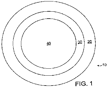
FIG. 1 shows schematically a bearing element in accordance with the
invention;
FIG. 2 shows a heating element in accordance with the invention of the
invention;
FIG. 3 shows a flame rod element in accordance with the invention;
FIG. 4 shows a thermal electric element in accordance with the invention;
FIG 5. shows a cutting blade system in accordance with the invention; and
FIG. 6 shows a piezoelectric ceramic element.
CA 02660573 2009-02-11
WO 2008/021508 PCT/US2007/018286
-8-
DETAILED DESCRIPTION
As discussed above, new methods are now provided for producing ceramic
elements that include injection molding of one or more layers or regions of
the
element.
As typically referred to herein, the term "injection molded," "injection
molding" or other similar term indicates the general process such as where a
material
(here a ceramic or pre-ceramic material) is injected or otherwise advanced
typically
under pressure into a mold in the desired shape of the ceramic element
typically
followed by cooling and subsequent removal of the solidified element that
retains a
replica of the mold.
In injection molding formation of elements of the invention, a ceramic
material (such as a ceramic powder mixture, dispersion or other formulation)
or a pre-
ceramic material or composition may be advanced into a mold element.
In suitable fabrication methods of the invention, an integral element having
regions of differing resistivities may be formed by sequential injection
molding of
ceramic or pre-ceramic materials having differing resisitivities.
Thus, for instance, a base element may be formed by injection introduction of
a material having a first resisitivity into a mold element that defmes a
desired base
shape such as a rod shape. The base element may be removed from such first
mold
and positioned in a second, distinct mold element and ceramic material having
differing resistivity - e.g. a conductive ceramic material - can be injected
into the
second mold to provide conductive region(s) of the element. In similar
fashion, the
base element may be removed from such second mold and positioned in a yet
third,
distinct mold element and ceramic material having differing resistivity - e.g.
a
resistive hot zone ceramic material - can be injected into the third mold to
provide
higher resistivity region(s) of the element.
A base ceramic element may comprise additional distinct ceramic composition
regions, including four or five or more distinct regions. For instance, such
an element
CA 02660573 2009-02-11
WO 2008/021508 PCT/US2007/018286
-9-
is disclospd in U.S. Patent Application Publication 2002/0150851 to Willkens,
which
describes ceramic igniters having four ceramic regions of distinct electrical
resistivity
,(conductive region of relatively low resistance, a power booster or
enhancement zone
of intermediate resistance, a heat sink region of distinct resistance, and a
hot or
ignition zone of relatively high electrical resistance). Those multiple,
distinct regions
may be produced by a plurality of multiple injection molding steps as
disclosed
herein.
Also, rather than use of a plurality of distinct mold elements as discussed
above, differing ceramic materials may be sequentially advanced or injected
into the
same mold element. For instance, a predetermined volume of a first ceramic
material
may be introduced into a mold element that defmes a desired base shape and
thereafter a second ceramic material of differing resisitivity may be applied
to the
formed base.
Ceramic material may be advanced (injected) into a mold element as a fluid
formulation that comprises one or more ceramic materials such as one or more
ceramic powders.
For instance, a slurry or paste-like composition of ceramic powders may be
prepared, such as a paste provided by admixing one or more ceramic powders
with an
aqueous solution or an aqueous solution that contains one or more miscible
organic
solvents such as alcohols and the like. A preferred ceramic slurry composition
for
extrusion may be prepared by admixing one or more ceramic powders such as
MoSi2,
SiC2 A1203, and/or AIN in a fluid composition of water optionally together
with one
or more organic solvents such as one or more aqueous-miscible organic solvents
such
as a cellulose ether solvent, an alcohol, and the like. The ceramic slurry
also may
contain other materials e.g. one or more organic plasticizer compounds
optionally
together with one or more polymeric binders.
A wide variety of shape-forming or inducing elements may be employed to
form an element, with the element of a configuration corresponding to desired
shape
CA 02660573 2009-02-11
WO 2008/021508 PCT/US2007/018286
-10-
of the formed element. For instance, to form a rod-shaped element, a ceramic
powder
paste may be injected into a cylindrical die element. To form a stilt-like or
rectangular-shaped element, a rectangular die may be employed.
After advancing ceramic material(s) into a mold element, the defined ceramic
part suitably may be dried e.g. in excess of 50 C or 60 C for a time
sufficient to
remove any solvent (aqueous and/or organic) carrier.
As mentioned above, it has been found that results and quality of the produced
element can be enhanced by good mating of the multiple injection molded
ceramic
regions, including good mating of the third (or further subsequent) injection
molded
portion with previously deposited first and second portions. In addition to
accurate
placement of subsequently molded portions, mating of characteristics of
adjacent
distinct ceramic regions can ensure a higher quality formed element. For
instance, it
can desirable that the binder compositions used for ceramic compositions of
distinct
regions are similar in components, viscosity and other characteristics.
It also can be desirable that the first deposited ceramic composition region
have a relatively enhanced structural integrity as applied in a green state
with binder
composition to be thereby resistant to deformation upon injection molding of
subsequent, adjoining ceramic regions. For instance, the first deposited
ceramic
composition may comprise a binder additive such as a polymer e.g.
polypropylene
that can provide greater structural integrity to the deposited ceramic region.
The first
deposited region also may be formed with topography (e.g. cross-hatched
surface)
that will mate with and provide good adherence to a subsequently applied
adjacent
ceramic region.
As discussed above, good mating of the second, third or further injection
molded portions of the ceramic element can be facilitated by effective air
removal
from the site where the ceramic material is being deposited via injection
molding. For
example, effective venting (removal) of air from the deposition site can aid
good
mating of the ceramic material being deposited with previously deposited
ceramic
CA 02660573 2009-02-11
WO 2008/021508 PCT/US2007/018286
-11-
element portions. Such venting can be accomplished by various methods,
including
maintaining a slight negative pressure (vacuum line) in the general area that
ceramic
material is being deposited. Additionally, delivery speed of the ceramic
material
should not exceed a level where effective air removal is inhibited.
It also has been found that injection molding deposition of second, third and
further higher order portions should be done whereby previously deposited
element
portions are not deformed to thereby maintain the structural integrity of the
produced
element.
The examples which follow describe preferred injection molding processes.
Referring now to the drawings, FIG. 1 shows in schematic cross-section a
bearing element 10 with multiple, distinct ceramic regions 20, 30 and 40 that
each
differ in thermal expansion characteristics (i.e. differing coefficients of
thermal
expansion(CTE)), for instance where outer region 10 has a relatively low CTE,
middle region 20 has an intennediate relative CTE value, and inner or core
region 30
has the highest relative CTE value of the element.
FIG. 2 shows in a schematic top view a heater plate element 50 which includes
concentric ceramic regions 60, 70 and 80. Heater plate element 50 may be for
example a cigarette lighter for a motor vehicle. As depicted in FIG. 2.,
heater plate
element 50 may comprise conductive zones 60 and 80 with an interposed
resistive
(hot) zone 70.
FIG. 3 shows schematically a ceramic flame rod or flame rectifier100 which
comprises multiple, distinct ceramic regions 110, 120 and 140. Region 110 is
electrically conductive and region 120 is a resistive (hot) zone to provide a
heating
element particularly an igniter. Flame detection element 140 is spaced from
regions
110 and 120 by void area 130. Detection element 140 is suitably a conductive
ceramic region which in use forms a circuit between a flame and ground.
CA 02660573 2009-02-11
WO 2008/021508 PCT/US2007/018286
-12-
FIG. 4 shows schematically thermal electric ceramic element 150 which
includes multiple, distinct ceramic regions of conductor regions 160, N-type
region
170, P-type region 180 and support portion 190.
FIG. 5 shows schematically a heated cutting blade 200 which comprises
multiple, distinct ceramic regions of insulating regions 210, 240 and 270,
conductive
regions 220 and 280, resistive (hot) regions of 230 and 260, and cutting
surface 290
(which suitably would be an insulating composition).
FIG. 6 shows a piezoelectric ceramic element 300 which may include
multiple, distinct ceramic regions. Piezoelectric ceramic element 300 may be
suitably
a piezoelectric ceramic oscillator rod element which includes electrode
regions 310
and piezoelectric ceramic rod regions 320. Such an element 300 may be suitably
a
component of a ceramic gyro device (which can detect various movement) where
the
vibrating element comprises a cylindrical piezoelectric ceramic oscillator rod
300. In
use of certain systems, when voltage is applied to the piezoelectric ceramic
oscillator
rod, the rod torsionally vibrates. When the rod 300 rotates, the rod can
output voltage
in proportion to the rotational velocity.
As discussed above, the elements and devices depicted in FIGS. 1 through 6
are produced through injection molding of multiple ceramic compositions to
form the
element. Once the element is formed by such injection molding processing, the
element may be further processed as desired. For example, the formed element
may
be further densified such as under conditions that include elevated
temperature and
pressure.
Additionally, ceramic regions of differing composition or properties (e.g.
differing resistivity) may be applied to a formed base element by procedures
other
than injection molding, e.g. a base element may be dip coated in a ceramic
composition slurry to provide a region with appropriate masking of device
regions as
desired. For such dip coating applications, a slurry or other fluid-like
composition of
the ceramic composition may be suitably employed. The slurry may comprise
water
CA 02660573 2009-02-11
WO 2008/021508 PCT/US2007/018286
-13-
and/or polar organic solvent carriers such as alcohols and the like and one or
more
additives to facilitate the formation of a uniform layer of the applied
ceramic
composition. For instance, the slurry composition may comprise one or more
organic
emulsifiers, plasticizers, and dispersants. Those binder materials may be
suitably
removed thermally during subsequent densification of the ceramic element.
Significantly, methods of the invention can facilitate fabrication of ceramic
elements and devices of a variety of configurations as may be desired for a
particular
application. To provide a particular configuration, an appropriate shape-
inducing
mold element is employed through which a ceramic composition (such as a
ceramic
paste) may be injected.
A wide va'riety of ceramic compositions may be employed to form elements of
the invention. For instance, as discussed above, ceramic compositions of
differing
resistivies may be employed in a particular element. Generally preferred
highly
resistive (hot) zone or region ceramic compositions comprise two or more
components of 1) conductive material; 2) semiconductive material; and 3)
insulating
material. Conductive (cold) and insulative (heat sink) regions may be
comprised of
the same components, but with the components present in differing proportions.
Typical conductive materials include e.g. molybdenum disilicide, tungsten
disilicide,
nitrides such as titanium nitride, and carbides such as titanium carbide.
Typical
semiconductors include carbides such as silicon carbide (doped and undoped)
and
boron carbide. Typical insulating materials include metal oxides such as
alumina or a
nitride such as A1N and/or Si3N4.
As referred to herein, the term electrically insulating material indicates a
material having a room temperature resistivity of at least about 1010 ohms-cm.
The
electrically insulating material component of elements of the invention may be
comprised solely or primarily of one or more metal nitrides and/or metal
oxides, or
alternatively, the insulating component may contain materials in addition to
the metal
oxide(s) or metal nitride(s). For instance, the insulating material component
may
additionally contain a nitride such as aluminum nitride (A1N), silicon
nitride, or boron
CA 02660573 2009-02-11
WO 2008/021508 PCT/US2007/018286
-14-
nitride; a rare earth oxide (e.g. yttria); or a rare earth oxynitride. A
preferred added
material of the insulating component is aluminum nitride (A1N).
As referred to herein, a semiconductor ceramic (or "semiconductor") is a
ceramic having a room temperature resistivity of between about 10 and 108 ohm-
cm.
If the semiconductive component is present as more than about 45 v/o of a hot
zone
composition (when the conductive ceramic is in the range of about 6-10 v/o),
the
resultant composition becomes too conductive for high voltage applications
(due to
lack of insulator). Conversely, if the semiconductor material is present as
less than
1o about 10 v/o (when the conductive ceramic is in the range of about 6-10
v/o), the
resultant composition becomes too resistive (due to too much insulator).
Again, at
higher levels of conductor, more resistive mixes of the insulator and
semiconductor
fractions are needed to achieve the desired voltage. Typically, the
semiconductor is a
carbide from the group consisting of silicon carbide (doped and undoped), and
boron
carbide. Silicon carbide is generally preferred.
As referred to herein, a conductive material is one which has a room
temperature resistivity of less than about 10"2 ohm-cm. If the conductive
component
is present in an amount of more than 35 v/o of the hot zone composition, the
resultant
ceramic of the hot zone composition, the resultant ceramic can become too
conductive. Typically; the conductor is selected from the group consisting of
molybdenum disilicide, tungsten disilicide, and nitrides such as titanium
nitride, and
carbides such as titanium carbide. Molybdenum disilicide is generally
preferred.
In general, preferred hot (resistive) zone compositions include (a) between
about 50 and about 80 v/o of an electrically insulating material having a
resistivity of
at least about 1010 ohm-cm; (b) between about 0 (where no semiconductor
material
employed) and about 45 v/o of a semiconductive material having a resistivity
of
between about 10 and about 108 ohm-cm; and (c) between about 5 and about 35
v/o of
3o a metallic conductor having a resistivity of less than about 10"2 ohm-cm.
Preferably,
the hot zone comprises 50-70 v/o electrically insulating ceramic, 10-45 v/o of
the
semiconductive ceramic, and 6-16 v/o of the conductive material. For at least
certain
CA 02660573 2009-02-11
WO 2008/021508 PCT/US2007/018286
-15-
applications, a specifically preferred hot zone composition contains 10 v/o
MoSi2, 20
v/o SiC and balance AIN or A1203.
Preferred cold or conductive zone regions include those that are comprised of
e.g. A1N and/or A1203 or other insulating material; SiC or other semiconductor
material; and MoSi2 or other conductive material. However, cold zone regions
will
have a significantly higher percentage of the conductive and semiconductive
materials
(e.g., SiC and MoSiZ) than the hot zone. For at least certain applications, a
preferred
cold zone composition comprises about 15 to 65 v/o aluminum oxide, aluminum
nitride or other insulator material; and about 20 to 70 v/o MoSia and SiC or
other
conductive and semiconductive material in a volume ratio of from about 1:1 to
about
1:3. For many applications, more preferably, the cold zone comprises about 15
to 50
v/o AIN and/or A1203, 15 to 30 v/o SiC and 30 to 70 v/o MoSia. For ease of
manufacture of a particular element, preferably the cold zone composition is
formed
of the same materials as the hot zone composition, with the relative amounts
of
semiconductive and conductive materials being greater. For certain
application, a
specifically preferred cold zone composition contains 20 to 35 v/o MoSiz, 45
to 60 v/o
SiC and balance either A1N and/or A1203.
Insulative ceramic regions of an element may mate with a conductive zone or
a hot zone, or both. Preferably, a sintered insulator region has a resistivity
of at least
about 1014 ohm-cm at room temperature and a resistivity of at least 104 ohm-cm
at
operational temperatures and has a strength of at least 150 MPa. Preferably,
an
insulator region has a resistivity at operational (ignition) temperatures that
is at least 2
orders of magnitude greater than the resistivity of the hot zone region.
Suitable
insulator compositions comprise at least about 90 v/o of one or more aluminum
nitride, alumina and boron nitride. For certain applications, a specifically
preferred
insulator composition consists of 60 v/o A1N; 10 v/o A1203; and balance SiC.
The following non-limiting examples are illustrative of the invention. All
documents mentioned herein are incorporated herein by reference in their
entirety.
CA 02660573 2009-02-11
WO 2008/021508 PCT/US2007/018286
-16-
Example 1: Device fabrication
Powders of a resistive composition (22vo1% MoSi2, remainder A1203) and an
insulating composition (100vo1% A1203 ) were mixed with an organic bonder
(about
6-8wt% vegetable shortening, 2.4wt% polystyrene and 2-4 wt% polyethylene) to
form
two pastes with about 62 vol % solids. The two pastes were loaded into two
barrels of
a co-injection molder. A first shot filled a half-cylinder shaped cavity with
insulating
paste forming the supporting base with a fin running along the length of the
cylinder.
The part was removed from the first cavity, placed in a second cavity and a
second
shot filled the volume bounded by the first shot and the cavity wall core with
the
conductive paste. The molded part which forms a hair-pin shaped conductor with
insulator separating the two legs. The rod was then partially debindered at
room
temperature in an organic solvent dissolving out 10 wt% of the added 10-16
wt%.
The part was then thermally debindered in flowing inert gas (N2) at 300-500 C
for 60
hours to remove the remainder of the residual binder. The debindered part was
densified to 95-97% of theoretical at 1800-1850 C in Argon. The densified part
was
cleaned up by grit-blasting. When the two legs of the igniter device are
connected to
a power supply at a voltage of 36V, the hot-zone attained at temperature of
about
1300 C.
Example 2: Additional device fabrication
Powders of a resistive composition (22 vol% MoSi2, remainder A1203) and -
an insulating composition (5vol%SiC, remainder A1203) were mixed with an
organic
bonder (about 6-8wt% vegetable shortening, 2.4wt% polystyrene and 2-4 wt%
polyethylene) to form two pastes with about 62 vol % solids. The two pastes
were
loaded into two barrels of a co-injection molder. A first shot filled a half-
cylinder
shaped cavity with insulating paste forming the supporting base with a fin
rnnõiõg
along the length of the cylinder. The part was removed from the first cavity,
placed
in a second cavity and a second shot filled the volume bounded by the first
shot and
the cavity wall core with the conductive paste. The molded part which forms a
hair-
3o pin shaped conductor with insulator separating the two legs. The rod was
then
partially debindered at room temperature in an organic solvent dissolving out
10 wt%
of the added 10-16 wt%. The part was then thermally debindered in flowing
inert gas
CA 02660573 2009-02-11
WO 2008/021508 PCT/US2007/018286
-17-
such as N2 at 300-500 C for 60 hours to remove the remainder of the residual
binder.
The debindered parts were densified to 95-97% of theoretical at 1800-1850 C in
Argon. Densified parts were cleaned up by grit-blasting. When the two legs of
the
igniters are=connected to a power supply at voltages ranging from of 120V, the
hot-
zone attained at temperature of about 1307 C.
Example 3: Additional device fabrication.
Powders of a resistive composition (22vol% MoSi2, 20 vol% SiC, remainder
A1243) and an insulating composition (20vo1% SiC, remainder A1203) were mixed
lo with about 15 wt% polyvinyl alcohol to form two pastes with about 60 vol %
solids.
The two pastes were loaded into two barrels of a co-injection molder. A first
shot
filled a cavity that had an hour-glass shaped cross-section with insulating
paste
forming the supporting base. The part was removed from the first cavity,
placed in a
second cavity and a second shot filled the volume bounded by the first shot
and the
cavity wall core with the conductive paste. The molded part which forms a hair-
pin
shaped conductor with insulator separating the two legs was then partially
debindered
in tap water dissolving out 10 wt% of the added 10-16 wt%. The part was then
thermally debindered in flowing inert gas (NZ) at 500 C for 24h to remove the
remainder of the residual binder. The debindered part was densified to 95-97%
of
theoretical at 1800-1850 C in Argon. The densified part was cleaned up by grit-
blasting. When the two legs of the igniter are connected to a power supply at
a
voltage of 48V, the hot-zone attained at temperature of about 1300 C.
Example 4: Further device fabrication
Powders of a resistive composition (20 vol% MoSi2, 5 vol% SiC, 74vo1%
A1203 and 1 vol% Gd203), a conductive composition (28 vol% MoSi2, 7 vol% SiC ,
64vo1% A1203 and 1 vol% Gd203) and an insulating composition (10 vol% MoSi2,
89 vol% A1203 and 1 vol% Gd203) were mixed with 10-16 wt% organic binder
(about 6-8 wt% vegetable shortening, 2-4 wt% polystyrene and 2-4 wt%
polyethylene) to form three pastes with about 62-64 vol% solids loading. The
three
pastes were loaded into the barrels of a co-injection molder. A first shot
filled a
cavity that had an hour-glass shaped cross-section with the insulating paste
forming
CA 02660573 2009-02-11
WO 2008/021508 PCT/US2007/018286
-18-
the supporting base. The part was removed from the first cavity and placed in
a
second cavity. A second shot filled the bottom half of the volume bounded by
the
first shot and the cavity wall with the conductive paste. The part was removed
from
the second cavity and placed in a third cavity. A third shot filled the volume
bounded
by the first shot, second shot and the cavity wall with resistive paste
forming a hair-
pin shaped resistor separated by the insulator and connected to conductive
legs also
separated by the insulator. The molded part was the partially debindered in n-
propyl
bromide dissolving out 10 wt% of the added 10-16 wt%. The part was then
thermally
debindered in slowing Ar or N2 at 500 C for 24h to remove the remaining binder
and
densified to 95-97% of theoretical at 1750 C in Argon at 1 atm pressure. When
the
two conductive legs of the igniter are connected to a power supply of a
voltage of
120V, the hot-zone (i.e. the resistive zone) attained a temperature of 1300 C.
Example 5: Further device fabrication
Powders of a resistive composition (21.5 vol% MoSi2, 5 vol% SiC, remainder
A1Z03), a conductive composition (28 vol% MoSi2, 7 vol% SiC, remainder A1203)
and insulating composition (10 vol % MoSi2a remainder A1203) were mixed with
about 12 wt% paraffm-wax based binder to form three pastes with about 64 vol%
solids loading. A higher melting wax composition was used to increase the
thermal
stability of the green (as-molded) the first shot i.e. supporting member (in
this case the
insulating component). The three pastes were loaded into the barrels of a co-
injection
molder to whose mold-fra.me were attached the three cavities corresponding to
each
shot. The first shot filled a cavity that had a nearly rectangular cross-
section tapering
along the length in both directions with the insulating paste, forming the
supporting
member. The part was removed from the first cavity and placed in a second
cavity.
The second shot filled a cavity bounded by the first shot and the cavity wall
with the
conductive paste. The part was removed from the second cavity and placed in a
third
cavity. A third shot filled the volume bounded by the first shot, second shot
and the
cavity wall with the resistive paste fonning a hair-pin shaped section
separated by the
insulating support and connected to the conductive sections also separated by
the
insulating support. The molded part was partially debindered in tap water
removing 3-
4 wt% of the added 12 wt% binder. The part was then thermally debindered in
CA 02660573 2009-02-11
WO 2008/021508 PCT/US2007/018286
-19-
flowing Argon at 300 C to 500C for 24h to remove the remaining binder and
densified to greater than 97% of theoretical density by gas pressure sintering
at
1750 C under maximum pressure of 3000psi. When the conductive legs of the
densified igniter are connected to a power supply of voltage 12V, the hot-zone
( i.e.
the resistive zone) attained a temperature of 1280-1320 C.
The invention has been described in detail with reference to particular
embodiments thereof. However, it will be appreciated that those skilled in the
art,
upon consideration of this disclosure, may make modification and improvements
1o within the spirit and scope of the invention.