Note: Descriptions are shown in the official language in which they were submitted.
CA 02662747 2009-03-05
WO 2008/030459 PCT/US2007/019340
INSULATED ELECTRICAL BUSHING AND METHOD OF PRODUCING THE SAME
BACKGROUND OF THE INVENTION
[0001] This
invention relates to insulated electrical bushings and more
particularly to sealing systems for electrical conductors of insulated
electrical
bushings.
[0002] An
insulated electrical bushing is used in an electrical device, such as
a distribution transformer, to secure an electrical conductor to a housing of
the
device. Typically, an electrical conductor of an electrical bushing extends
through an
opening in a housing and is used to connect the internals of an electrical
device to
the outside world. A conventional electrical bushing includes an exterior
insulating
body having a mounting flange for securing the insulated electrical bushing to
the
exterior of a housing of an electrical device. A centrally-disposed electrical
conductor
is secured inside the insulating body and extends through an opening in the
housing.
An outer end of the electrical conductor protrudes from the exterior
insulating body
and is adapted for connection to an exterior connector device, such as an
elbow
connector. An inner end of the electrical conductor is connected to internal
electrical
components of the electrical device, such as windings, directly, or through a
second
electrical conductor.
[0003] An
insulating body of an electrical bushing may be comprised of a
ceramic material or a polymeric material. In many conventional electrical
bushings
composed of polymeric material, the electrical conductor is secured inside a
pre-
formed insulating body using an adhesive, 0-rings and/or heat shrink tubing.
An
example of such a conventional insulated electrical bushing is disclosed in
U.S.
Patent No. 6,515,232 to Forster. In the Forster patent, a conductor is
disposed in a
pre-formed insulating body comprised of glass-reinforced epoxy or a silica-
filled
cycloaliphatic resin system. Asphalt is poured between the conductor and the
insulating body and 0-rings and spring retaining gaskets are disposed at the
top and
bottom ends of the insulating body.
[0004] Some
conventional insulated electrical bushings are formed in a much
simpler manner by molding an insulating body directly over a conductor, such
as is
disclosed in U.S. Patent No. 4,965,407 to Hamm and U.S. Patent No. 5,281,767
to
West et al. In the West et al. patent, the conductor is sandblasted before it
is
molded into the insulating body.
CA 02662747 2014-08-13
2
[0005] Although molding an insulating body directly over a conductor is
much
simpler than using 0-rings and gaskets, the seal formed by a conventional over
molding process tends to be less robust and often still requires the use of an
adhesive.
[0006] It would therefore be desirable, to provide an electrical bushing
that is
simple to manufacture and has a robust seal. The present invention is directed
to
such an electrical bushing and a method for manufacturing the same.
SUMMARY OF THE INVENTION
[0007] In accordance with the present invention, an electrical bushing is
provided. The electrical bushing includes an insulating body secured to a
metal
conductor having a first embossment region and a second embossment region. The
first embossment region has a pattern of protuberances and the second
embossment
region has at least one annular ring. The protuberances of the first
embossment
region are not annular rings.
[0008] Also provided in accordance with the invention is a method of
forming
an electrical bushing. In accordance with the method, a metal conductor is
provided
having a first embossment region and a second embossment region. The first
embossment region has a pattern of protuberances and the second embossment
region has at least one annular ring. The protuberances of the first
embossment
region are not annular rings. A plastic insulating body is molded over the
conductor.
According to an aspect of the present invention, there is provided an
electrical bushing comprising:
a metal conductor having a first embossment region, a second
embossment region and a third embossment region separated from the first and
second
embossment regions, the first and third embossment regions each being
comprised of a
pattern of protuberances and the second embossment region comprising at least
one
annular ring, wherein the protuberances of the first embossment region are not
annular
rings; and
an insulating body secured to the conductor and being disposed over the
first, second and third embossment regions.
According to another aspect of the present invention, there is provided a
method of forming an electrical bushing comprising:
providing a metal conductor having a first embossment region, a second
embossment region and a third embossment region separated from the first and
second
CA 02662747 2014-08-13
2a
embossment regions, the first and third embossment regions each being
comprised of a
pattern of protuberances and the second embossment region comprising at least
one
annular ring, wherein the protuberances of the first embossment region are not
annular
rings; and
molding a plastic insulating body over the conductor so as to be disposed
over the first, second and third embossment regions.
BRIEF DESCRIPTION OF THE DRAWINGS
[0009] The features, aspects, and advantages of the present invention will
become better understood with regard to the following description, appended
claims,
and accompanying drawings where:
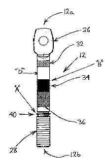
[0010] Fig. 1 shows an exploded view of an electrical bushing assembly
disposed in front of a wall of an electrical device, wherein the electrical
bushing
assembly includes an electrical bushing constructed in accordance with a first
embodiment of the present invention;
[0011] Fig. 2 shows an inner end perspective view of the electrical bushing
of
the first embodiment;
[0012] Fig. 3 shows a side view of a conductor of the electrical bushing of
the
CA 02662747 2009-03-05
WO 2008/030459 PCT/US2007/019340
3
first embodiment;
[0013] Fig. 4 shows an enlarged portion of the conductor of the electrical
bushing of the first embodiment, the portion being identified by the letter
"A" in Fig. 3;
[0014] Fig. 5 shows an enlarged portion of the conductor of the electrical
bushing of the first embodiment, the portion being identified by the letter
"B" in Fig. 3;
[0015] Fig. 6 shows a sectional view of a mold containing the conductor of
the
electrical bushing of the first embodiment;
[0016] Fig. 7 shows a side view of a conductor of an electrical bushing
constructed in accordance with a second embodiment of the present invention;
[0017] Fig. 8 shows an enlarged portion of the conductor of the electrical
bushing of the second embodiment, the portion being identified by the letter
"A" in Fig.
7;
[0018] Fig. 9 shows a perspective view of a conductor of an electrical
bushing
constructed in accordance with a third embodiment of the present invention;
[0019] Fig. 10 shows a side view of a conductor of the electrical bushing
of the
third embodiment;
[0020] Fig. 11 shows an enlarged portion of the conductor of the electrical
bushing of the third embodiment, the portion being identified by the letter
"A" in Fig. 10;
and
[0021] Fig. 12 shows an enlarged portion of an embossment region having
diamond knurls.
[0022]
DETAILED DESCRIPTION OF ILLUSTRATIVE EMBODIMENTS
[0023] It should be noted that in the detailed description that follows,
identical
components have the same reference numerals, regardless of whether they are
shown in different embodiments of the present invention. It should also be
noted
that in order to clearly and concisely disclose the present invention, the
drawings
may not necessarily be to scale and certain features of the invention may be
shown
in somewhat schematic form.
[0024] Referring now to Figs. 1 and 2, there is shown an electrical bushing
10
constructed in accordance with a first embodiment of the present invention.
The
bushing 10 may be a low voltage bushing adapted for use in a distribution
transformer. The bushing 10 includes a conductor 12 and an insulating body 14.
As
CA 02662747 2009-03-05
WO 2008/030459 PCT/US2007/019340
4
will be described in more detail below, the insulating body 14 is molded
around the
conductor 12 in an injection over-molding process.
[0025] The insulating body 14 is composed of a dielectric plastic and more
particularly a dielectric thermoplastic. Examples of dielectric thermoplastics
that may
be used to form the insulating body 14 include polyphthalamide or high
temperature
nylon (HTN), polyethylene terephthalate (PET) and polybutylene terephthalate
(PBT). The insulating body 14 includes a triangular flange 16 disposed around
a
cylindrical main section 18. Mounting openings 20 are located at the three
corners -
of the flange 16, respectively, and extend through the flange 16. At the
juncture of
the main section 18 and the flange 16, an annular recess 24 is formed in an
inner
surface 16a of the flange 16 and extends around the main section 18. As will
be
described below, the annular recess 24 functions as a gasket seat. The flange
16
divides the main section 18 into an inner portion 18a and an outer portion
18b.
[0026] Referring now to Figs. 3, 4 and 5, the conductor 12 is elongated
and
has a first or inner end 12a and a second or outer end 12b. The conductor 12
is
composed of a conductive metal, such as copper. The conductor 12 has a
connection spade 26 at the inner end 12a and a threaded portion 28 at the
outer
end 12b. The threaded portion 28 has a continuous helical thread. Between the
threaded portion 28 and the connection spade 26, a plurality of different
embossment regions are formed in the conductor 12. More particularly, there is
a
first embossment region 32, a second embossment region 34, a third embossment
region 36 and a fourth embossment region 40.
[0027] The first embossment region 32 and the third embossment region 36
each comprise a pattern of protuberances that extend around the circumference
of
the conductor 12. The protuberances may be straight knurls, diagonal knurls,
diamond knurls, dimples, or other types of projections raised from the surface
of the
conductor 12. Each individual protuberance does not extend around the
circumference of the conductor 12, i.e., is not an annular ring. Straight
knurls extend
in a longitudinal direction of the conductor 12, while diagonal knurls extend
obliquely
to a longitudinal direction of the conductor 12. In the embodiment shown in
Figs. 1-6,
the first embossment region 32 comprises diagonal knurls having 12 teeth per
linear
inch (TPI) and the third embossment region 36 comprises diamond knurls having
12
TPI with a 30 helix angle and a 900 tooth form. In this embodiment, the third
CA 02662747 2009-03-05
WO 2008/030459 PCT/US2007/019340
embossment region 36 is more than twice as long as the first embossment region
32. A close up view of a portion of the third embossment region 36 is shown in
Fig.
12. The protuberances comprise diamond knurls 42 that are spaced-apart and
arranged in bands.
[0028] The second embossment region 34 comprises a plurality of annular
rings 44 separated by a plurality of annular valleys 46. As expressed in TPI
(where
one ring 44 is considered a tooth), the rings 44 are provided in a quantity
that is in a
range of from about 10 TPI to about 14 TPI. The quantity and size of the rings
44 is
dependent on the viscosity and flow properties of the dielectric plastic that
makes up
the insulating body 14. More particularly, the valleys 46 must be shallow
enough to
permit a dielectric plastic of a particular viscosity to flow into the valleys
46 and fill
them during the molding process. In one embodiment, the insulating body 14 is
composed of high temperature nylon and the rings 44 are provided in a quantity
of
12 TPI. More particularly, in this embodiment, seven rings 44 are provided and
the
diameter of each of the rings 44 is about 0.611 inches and the diameter of the
conductor 12 in each of the valleys 46 is about 0.518 inches. In this
embodiment,
the diameter of the conductor 12 at the location denoted by the "D" in Fig. 3
is 0.56
inches.
[0029] The fourth embossment region 40 has a single annular ring 50
disposed between two valleys 52. The ring 50 has a larger diameter than the
rings
44. In the embodiment described above where the rings 44 each have a diameter
of
about 0.611 inches, the ring 50 has a diameter of about 0.699 inches and the
diameter of the conductor 12 in each of the valleys 52 is 0.50 inches. During
the
molding process, the ring 50 forms a shut off point where the flow of molten
plastic is
pinched off, as will be described further below.
[0030] The threaded portion 28 and the first, second, third and fourth
embossment regions 32-40 are all produced from a conductor blank (not shown)
by
roll forming. The conductor. blank includes the connection spade 26 joined to
a
cylindrical body having a smooth outer surface. The body is deformed by
different
shaped rollers to form the threads in the threaded portion 28 and the
different
embossments of the first, second, third and fourth embossment regions 32-40.
[0031] Although the conductor 12 is shown as having four embossment
regions (32-40), it should be appreciated that the conductor 12 may be
provided with
CA 02662747 2009-03-05
WO 2008/030459 PCT/US2007/019340
6
a greater or lesser number of embossment regions, or a different combination
of
different types of embossment regions. For example, the first embossment
region 32
may be replaced with an embossment region having a singular annular ring with
the
same dimensions as the ring 50, or an embossment region having a plurality of
annular rings having the dimensions and spacing of the rings 44. However, it
has
been found that a combination of at least one embossment region having knurls
(such as diamond knurls) and at least one embossment region having at least
one
annular ring provides a robust sealing system.
[0032] Referring now to Fig. 6, the bushing 10 is formed by disposing the
conductor 12 in a mold 56 of an injection molding machine. The mold 56
includes a
pair of platens 58 (at least one of which is movable) that cooperate to define
a cavity
60, which is configured to hold the conductor 12 and to shape the molten
thermoplastic so as to form the insulating body 14 thereon. The conductor 12
is
positioned such that the first, second, third and fourth embossment regions 32-
40
are disposed in the cavity 60. Upper and lower portions pf the conductor 12
extend
out of the cavity 60 through upper and lower passages formed between the two
platens 58. The lower passages cooperate with the ring 50 to form shut off
points
62 where the flow of molten thermoplastic is pinched off.
[0033] With the conductor 12 so disposed in the cavity 60, molten =
thermoplastic resin is injected into the cavity 60 under pressure. The molten
thermoplastic flows over the conductor 12 and into the recesses of the first,
second,
third and fourth embossment regions 32-40. Thus, in the second embossment
region 34, the molten thermoplastic flows into and fills the valleys 46. The
molten
thermoplastic also flows into and fills an uppermost one of the valleys 52 and
flows
around and over the ring 50 and is pinched off at the shut-off points 62.
After a
predetermined period of time, the injection of the molten thermoplastic into
the cavity
60 is shut-off and the thermoplastic in the cavity 60 is allowed to cool. When
the
thermoplastic is sufficiently cooled, the mold 56 is opened and the conductor
12 with
the insulating body 14 formed thereon is removed.
[0034] Referring back to Fig. 1, the fully constructed bushing 10 may be
mounted to a wall 68 of an electrical device, such as a distribution
transformer. The
wall 68 includes a circular opening 70 through which the bushing 10 extends
into the
electrical device. Three threaded bolts 72 extend from the wall 68 and are
disposed
CA 02662747 2009-03-05
WO 2008/030459 PCT/US2007/019340
7
around the opening 70. The bolts 72 are arranged in a configuration that is
substantially identical to the configuration of the mounting openings 20 in
the flange
16 of the bushing 10. The bushing 10 is mounted to the wall 68 by first
disposing an
annular gasket 74 in the recess 24 of the flange 16 and then aligning the
mounting
openings 20 with the bolts 72, respectively. The bushing 10 is then moved
inward
toward the wall 68 so that the bolts 72 pass through the mounting openings 20
and
the connection spade 26 and the inner portion 18a of the main section pass
through
the opening 70. When the gasket 74 contacts the wall 68, the inward movement
of
the bushing 10 is stopped and sets of mounting nuts and washers (not shown)
are
threadably disposed over the bolts 72, respectively, to secure the bushing to
the wall
68. With the bushing 10 so mounted, the connection spade 26 is disposed inside
the electrical device (e.g. a distribution transformer) and may be connected
to an
internal electrical component of the electrical device (e.g. low voltage
leads). An
external circuit may be connected to the conductor 12 of the bushing 10 using
a
brass contact nut 76, which is threadably disposed over the threaded portion
28 of
the conductor 12.
[0035] The first,
second, third and fourth embossment regions 32-40 provide
both a mechanical connection and a gas tight seal between the conductor 12
and,
the insulating body 14.
[0036] Referring
now to Figs. 7 and 8, there is shown a conductor 80 of an
electrical bushing constructed in accordance with a second embodiment of the
present invention. An insulating body (not shown) is molded over the conductor
80.
[0037] The
conductor 80 is composed of a conductive metal, such as copper.
The conductor 80 is elongated and includes a middle section 82 disposed
between a
first threaded portion 84 and a second threaded portion 86. The first and
second
threaded portions 84, 86 each have a continuous helical thread. The middle
section
82 includes a first embossment region 88, a second embossment region 90, a
third
embossment region 92 and a fourth embossment region 94. The first and second
threaded portions 84, 86, and the first, second, third and fourth embossment
regions
88, 90, 92 and 94 are all produced by roll forming.
[0038] The first
embossment region 88 comprises a pattern of protuberances
disposed around the circumference of the conductor 80. The protuberances may
be
straight knurls, diagonal knurls, diamond knurls, dimples, or other types of
CA 02662747 2009-03-05
WO 2008/030459 PCT/US2007/019340
8
projections raised from the surface of the conductor 80. In the embodiment
shown in
Figs. 7 and 8, the first embossment region 88 comprises diamond knurls having
12
TPI with a 30 helix angle and a 90 tooth form. The first embossment region
88 is
produced by roll forming.
[0039] The second embossment region 90 and the fourth embossment region
94 each comprise a plurality of annular rings 98 separated by a plurality of
annular
valleys 100. As expressed in TPI (where one ring 98 is considered a tooth),
the
rings 98 are provided in a quantity that is in a range of from about 10 TPI to
about 14
.
TPI.
[0040] The third embossment region 92 comprises a single annular ring
102.
The ring 102 has a larger diameter than the rings 98. In one embodiment, the
ring
102 has a diameter of 0.630 inches and the rings 102 each have a diameter of
0.549 inches.
[0041] Referring now to Figs. 9, 10 and 11, there is shown a conductor
110 of
an electrical bushing constructed in accordance with a third embodiment of the
present invention. An insulating body (not shown) is molded over the conductor
110.
[0042] The conductor 110 is composed of a conductive metal, such as
copper, and is elongated. The conductor 110 includes a threaded end portion
112
and a body portion 114 having a plurality of embossment regions. The threaded
end
portion 112 has a continuous helical thread. The body portion 114 has a first
embossment region 116, a second embossment region 118 and a third embossment
region 120. The threaded end portion 112, and the first, second, and third
embossment regions 116, 118 and 120 are all produced by roll forming. An
axially-
extending bore 122 is formed in the body portion 114. Art annular flange 121
is
disposed around the bore 122 and is joined to the body portion 114.
[0043] The first and third embossment regions 116, 120 each comprise a
plurality of annular rings 124 separated by a plurality of annular valleys
126. As
expressed in TPI (where one ring 124 is considered a tooth), the rings 124 are
provided in a quantity that is in a range of from about 10 TPI to about 14
TPI.
[0044] The second embossment region 118 comprises a pattern of
protuberances disposed around the circumference of the conductor 110. The
protuberances may be straight knurls, diagonal knurls, diamond knurls,
dimples, or
other types of projections raised from the surface of the conductor 110. In
the
CA 02662747 2014-08-13
9
embodiment shown in Figs. 9 and 10, the second embossment region 118
comprises diamond knurls having 12 TPI with a 300 helix angle and a 90 tooth
form.
The second embossment region 118 is produced by roll forming.
10045] It is to
be understood that the description of the foregoing exemplary
embodiment(s) is (are) intended to be only illustrative, rather than
exhaustive, of the
present invention.