Note: Descriptions are shown in the official language in which they were submitted.
CA 02662854 2009-03-06
DESCRIPTION
OPTICAL CONNECTOR
TECHNICAL FIELD
[0001] The present invention relates to a PC-connectable
optical connector for optical communications, and more
particularly is suitable as a plug-in type optical connector
attached to a board member.
BACKGROUND ART
[0002] As one of optical connectors, which connect optical
fibers to each other, a FPC (Fiber Physical Contact) connector
is known as disclosed in a 16-core FPC connector with a shutter
utilizing a MU coupling structure (C-3-120, 2003 Electronics
Society Conference, the Institute of Electronics, Information
and Communication Engineers) . The appearance of the FPC
connector is schematically illustrated in Fig. 9, and its
connected state is illustrated in Fig. 10. Specifically, a FPC
connector 1 includes an optical jack 3 into which optical fibers
2 on one side are drawn and an optical plug 5 into which optical
fibers 4 on the other side are drawn. A connection block 6 is
provided in the optical jack 3. The connection block 6 has micro
holes, namely, connection holes 6a, each with an inner diameter
(for example, 126 pm when the optical fiber has an outer diameter
of 125 pm) slightly larger than an outer diameter (normally,
125 pm) of the optical fibers 2 and 4. The optical fibers 2
are inserted into the connection holes 6a from the base end side
of the connection block 6. The optical fibers 4, which are
- 1 -
CA 02662854 2009-03-06
placed on the optical plug 5 side and are to be inserted into
the connection holes 6a from the tip end side of the connection
block 6, are held in advance so as to project from a butting
surface 5a of the optical plug 5 which is to butt against a
butting surface 3a of the optical jack 3. When the butting
surface 5a of the optical plug 5 butts against that of the optical
jack 3 to thereby make connection therebetween, the optical
fibers 4 on the other side held by the optical plug 5 come into
contact with the optical fibers 2 on the one side held by the
optical jack 3. The contact takes place in the connection holes
6a of the connection block 6 of the optical jack 3. Then, the
optical fibers 4 on the other side are bent in the optical plug
by a buckling stress generated at this time. An elastic force
generated by bending of the optical fibers 4 on the other side
provides a PC state in which end surfaces 2a and 4b of the optical
fibers 2 and 4 on both sides are in pressure contact with each
other.
[0003] Additionally, in order to achieve the
aforementioned PC connection, a free length of the bendable and
deformable optical fiber 4 on the connection end side, the
optical fiber 4 being placed on the optical plug 5 side, is set
to, for example, 8 mm, and an extra length is set to, for example,
30 pm. Moreover, the buckling stress, which acts on the optical
fiber 4 at the time of PC connection, is set to, for example,
50 grams.
[0004] In Fig. 11, the appearance of a multi-core optical
- 2 -
CA 02662854 2009-03-06
connector utilizing the principle of the aforementioned FPC
connector is illustrated in a partially broken state. An
optical connector 100 is based on the coupling structure of a
duplex-core F14 (JIS C 5983) type, that is, a MU (Miniature
Unit-coupling) type optical connector disclosed in the
structure and characteristics of a high-density multi-core
plug-in optical connector having a self hold function (EMC91-39,
1991, Technical Report, the Institute of Electronics,
Information and Communication Engineers) In the optical
connector 100, an optical jack 200 and an optical plug 300 are
coupled to each other through an optical adaptor 400. The
frame-shaped optical adaptor 400 is provided with a guide member
401 projecting for defining the relative positions of the
optical jack 200 and the optical plug 300 with respect to the
optical adaptor 400. Correspondingly, guide grooves 201 and
301, which are engaged with the guide member 401, are formed
in the optical jack 200 and the optical plug 300, respectively.
This makes it possible to individually attach and detach the
optical jack 200 and the optical plug 300 to and from the optical
adaptor 400.
[0005] In an optical communication apparatus, an optical
connection system has been demanded in which a board member such
as a package substrate is moved relative to a backplane to
thereby automatically insert and withdraw optical fibers
attached to the backplane and optical fibers attached to the
board member.
- 3 -
CA 02662854 2009-03-06
[0006] However, the optical adaptor 400 of the
conventional MU optical connector 100 illustrated in Fig. 11
cannot be directly used in the backplane of the optical
communication apparatus in order to produce the FPC connector
functioning in the above-descried optical connection system.
As a result, a minimum contrivance is needed, for example, the
optical adaptor 400 is divided into two and one is attached to
the backplane and the other is attached to the board member.
However, it is revealed that there are many other problems to
be overcome.
DISCLOSURE OF THE INVENTION
[0007] The present invention has been made in view of the
aforementioned circumstances, and an object of the present
invention is to provide an optical connector which allows PC
connection and disconnection of optical fibers by an insertion
and withdraw operation between board members such as a backplane
and a package substrate in an optical communication apparatus.
[0008] An optical connector of the present invention
includes an optical plug to which a first optical fiber is
connected, a plug housing to which the optical plug is removably
attached, an optical jack to which a second optical fiber is
connected, the second optical fiber being connected to the first
optical fiber in a butting state, and a jack housing to which
the optical jack is removably attached, the jack housing being
detachably connected to the plug housing. The optical plug has
a box-shaped frame that houses a coupling end portion of the
- 4 -
CA 02662854 2009-03-06
first optical fiber in a surrounding manner. The optical jack
includes a connection block having a connection hole which
houses and holds a coupling end portion of the second optical
fiber on a base end side, and into which the first optical fiber
is inserted from a tip end side. The first optical fiber is
bent in the frame when the first optical fiber and the second
optical fiber are connected together. The optical connector
is characterized by including: housing position correction
means, which are provided in the plug housing and the jack
housing, for correcting displacement of relative positions
therebetween; housing connection means which are provided in
the plug housing and the jack housing, and which engage with
each other to connect the plug housing and the jack housing to
each other so that a coupling state between the first optical
f iber and the second opticalfiber can be maintained; connection
release means which is formed in at least one of the plug housing
and the jack housing, and which is capable of releasing the
connected state by the housing connection means; and frame
position correction means, which are provided in an inner side
of the frame of the optical plug and on the connection block
of the optical jack, for correcting displacement of relative
positions therebetween.
[0009] In the present invention, when the plug housing to
which the optical plug is attached is connected to the jack
housing to which the optical jack is attached, displacement of
relative positions therebetween is corrected by the housing
- 5 -
CA 02662854 2009-03-06
position correction means. Moreover, displacement of relative
positions between the frame of the optical plug and the
connection block of the optical jack is corrected by the frame
position correction means. As a result, the coupling end
portion of the first optical fiber held by the frame of the
optical plug is inserted into the connection hole from the tip
end side of the connection hole of the connection block of the
optical jack. Then, the first optical fiber pushes against the
second optical fiber housed on the base end side of the
connection hole, and a PC coupling state is achieved. This
state is held by the housing connection means, but the
connection release means is operated to thereby allow the plug
housing and the jack housing to be separated from each other,
so that the first optical fiber and the second optical fiber
are in an uncoupling state.
[0010] According to the optical connector of the present
invention, the plug housing and the jack housing can be
accurately connected to each other by the housing position
correction means when the first optical fiber and the second
optical fiber are coupled together. Further, it is possible
to more accurately position the frame of the optical plug and
the connection block of the optical jack by the frame position
correction means. As a result, the optical fiber can be surely
inserted into the connection hole of the connection block of
the optical jack to make it possible to maintain the PC
connection state with high reliability.
- 6 -
CA 02662854 2009-03-06
[0011] In the optical connector of the present invention,
the connection block may be housed in the frame of the optical
plug together with the frame position correction means, when
the optical plug is connected to the optical jack, whereby the
first optical fiber is inserted from the tip end side of the
connection hole.
[0012] As the housing position correction means, one of
the plug housing and the jack housing may have first inclined
surfaces which extend along a first direction perpendicular to
a direction where the plug housing and the jack housing are
attached to and detached from each other and which are
positioned more outwardly as they come closer to the tip end
side, and second inclined surfaces which extend along a second
direction perpendicular to the first direction and to the
direction where the plug housing and the jack housing are
attached to and detached from each other and which are
positioned more outwardly as they come closer to the tip end
side. The other of the plug housing and the jack housing may
have third inclined surfaces which correspond to the first
inclined surf aces and which are positioned more inwardly as they
come closer to the tip end side, and fourth inclined surfaces
which correspond to the second inclined surfaces and which are
positioned more inwardly as they come closer to the tip end side.
[0013] The frame position correction means may have a pair
of position correction members which are formed integrally with
the connection block, and which are fitted into the inner side
- 7 -
CA 02662854 2009-03-06
of the frame. Tip ends of these position correction members
may have: fifth inclined surfaces, which extend along a first
opening end edge of the frame, and which are positioned more
inwardly as they come closer to the tip end side; and sixth
inclined surfaces, which extend along a second opening end edge
perpendicular to the first opening end edge, and which are
positioned more inwardly as they come closer to the tip end side.
[0014] It is preferable that a facing distance between the
housing position correction means which are respectively formed
in the plug housing and the jack housing be set to be shorter
than a facing distance between the frame position correction
means which are respectively formed in the optical plug and the
optical jack. In this case, when the first optical fiber and
the second optical fiber are coupled together, the relative
positions between the plug housing and the jack housing is
roughly corrected. Then, the frame of the optical plug and the
connection block of the optical jack can be more accurately
positioned.
[00151 The optical jack can further include a frame which
holds the frame position correction means together with the
connection block, and positioning means for defining relative
positions between the housing position correction means and the
frame position correction means of the optical jack. In this
case, the relative position of the frame position correction
means with respect to the housing position correction means of
the optical jack can be accurately defined to make it possible
- 8 -
CA 02662854 2009-03-06
to achieve a stable connected state with high reliability.
[0016] One of the plug housing and the jack housing can
be fixed to a backplane, and the other can be fixed to a board
member. Particularly, it is preferable that the plug housing
be fixed to the backplane, and that the jack housing be fixed
to the board member. In this case, it is possible to achieve
a plug-in connection of the optical connector between a
backplane and a board member such as a package substrate.
Particularly, when the plug housing is fixed to the backplane
and the jack housing board is fixed to the board member, it is
possible to carry the board member to a location where a good
workability is obtained. As a result, it is possible to
facilitate maintenance and the like of the connection end
surface of the second optical fiber attached to the optical
jack.
BRIEF DESCRIPTION OF THE DRAWINGS
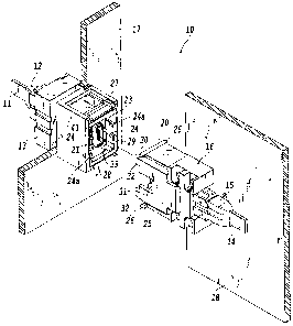
[0017] Fig. 1 is an isometric view illustrating an
appearance of an optical connector according to one embodiment
of the present invention and shows a separated state;
Fig. 2 is an isometric view illustrating an enlarged
appearance of exploded main parts of the optical connector
illustrated in Fig. 1;
Fig. 3 is a cross-sectional view schematically
illustrating an internal structure of the optical connector
illustrated in Fig. 1 and shows a non-connected state;
Fig. 4 is a cross-sectional view schematically
- 9 -
CA 02662854 2009-03-06
illustrating the internal structure of the optical connector
illustrated in Fig. 1 and shows a connected state;
Fig. 5 is an isometric view illustrating an enlarged
appearance of an optical jack in the optical connector
illustrated in Fig. 1;
Fig. 6 is an isometric view illustrating an exploded tip
end portion of the optical jack illustrated in Fig. 5;
Fig. 7 is a cross-sectional view schematically
illustrating the internal structure of the optical connector
illustrated in Fig. 1 and shows a middle state of connection
or separation;
Fig. 8 is an isometric view illustrating an appearance
of an optical connector according to another embodiment of the
present invention and shows a separated state;
Fig. 9 is an isometric view schematically illustrating
the principle of a FPC connector as a target of the present
invention and shows a separated state;
Fig. 10 is an isometric view schematically illustrating
the principle of the FPC connector as the target of the present
invention and shows a connected state;and
Fig. 11 is an isometric view illustrating an appearance
of multi-core optical connector as one example of a conventional
multi-core optical connector in a partially broken state and
shows a separated state.
BEST MODES FOR CARRYING OUT THE INVENTION
[0018] Specific description will be given of an embodiment
- 10 -
CA 02662854 2009-03-06
of the present invention with reference to Figs. 1 to 8. An
optical connector of the present invention is of a plug-in type
and attached to a board member. However, the present invention
is not limited to this embodiment, and it is needless to say
that the present invention can be applied to any other
technologies included within the spirit of the present
invention.
[0019] Fig. 1 illustrates an appearance of an optical
connector of the present embodiment. Fig. 2 illustrates an
enlarged appearance of exploded main parts thereof. Fig. 3
illustrates its cross sectional structure in a non-coupling
state. Fig. 4 illustrates its cross sectional structure in a
coupling state. An optical connector 10 in the present
embodiment includes an optical plug 12 to which first optical
fibers 11 are connected, a plug housing 13 to which the optical
plug 12 is removably attached, an optical jack 15 to which second
optical fibers 14 are connected, and a jack housing 16 to which
the optical jack 15 is removably attached. The plug housing
13 and the jack housing 16 are detachably connected to each other.
The first fibers 11 of the optical plug 12 and the second fibers
14 of the optical jack 15 achieve PC connection through the plug
housing 13 and the jack housing 16 while butting against one
another. In the present embodiment, the plug housing 13 is
attached to a backplane 17, and the jack housing 16 is fixed
to a package substrate 18. However, the attachment
relationship therebetween may be reversed as required. The
- 11 -
CA 02662854 2009-03-06
package substrate 18 is moved relatively to the backplane 17,
thereby allowing connection and disconnection between the
optical plug 12 and the optical jack 15. For this reason, on
a non-illustrated rack on which an optical communication
apparatus having the aforementioned backplane 17 is mounted,
a pair of upper and lower rails is provided which extends in
a direction facing the package substrate 18, namely, a direction
where the optical jack 15 is attached to and detached from the
optical plug 12. The package substrate 18 is movable in a
direction facing the backplane 17 along the pair of upper and
lower guide rails. The package substrate 18 can be fixed to
the backplane 17 by non-illustrated lock means. In this state,
the first optical fibers 11 and the second optical fibers 14
described above are coupled together.
[0020] Itisnoted that, in the present embodiment, sixteen
optical fibers 11 and sixteen optical fibers 14 are connected
to the optical plug 12 and the optical jack 15, respectively.
Coupling end portions of these are arranged in parallel with
one another at constant intervals.
[0021] In order to connect and disconnect the plug housing
13 and the jack housing 16, housing connection means, which are
engaged with each other, are provided in the plug housing 13
and the jack housing 16 to hold a connected state therebetween.
This maintains the PC coupling state between the first optical
fibers 11 and the second optical fibers 14. Moreover,
connection release means, which is capable of releasing the
- 12 -
CA 02662854 2009-03-06
connected state made by the housing connection means, is
provided in at least one of the plug housing 13 and the jack
housing 16.
[0022] The housing connection means in the present
embodiment includes: a pair of upper and lower locking hooks
20, which are projected to a frame 19 of the optical jack 15,
and which have tip end portions elastically deformable in a
vertical direction of Fig. 4; and a pair of upper and lower hook
locking portions 22 which are formed on a frame 21 of the optical
plug 12 to allow the tip end portions of these paired locking
hooks 20 to be locked. These hook locking portions 22 are formed
on tip end sides of frame-shaped sliders 23, which are slidably
fitted into the plug housing 13 in its longitudinal direction
(direction parallel to a direction where the optical plug 12
is attached to and detached from the plug housing 13) . Each
slider 23 has non-illustrated engaging portions that are
engaged with a part of a sliding surface between the slider 23
and the plug housing 13 so as to snap-fasten the plug housing
13 at its forward end. Moreover, in order to release the engaged
state of the engaging portions, a pair of hook portions 24 for
releasing engagement is provided in a protruding condition on
right and left sides of the front end portions of the sliders
23, respectively. The hook portions 24 have such inclined
surfaces 24a that gradually separate from an inner wall surface
of the plug housing 13 toward the tip end side. The hook
portions 24 are elastically deformable in right and left
- 13 -
CA 02662854 2009-03-06
directions, that is, in directions separating from the inner
wall surface of the plug housing 13. In right and left side
walls of the jack housing 16, notch portions 25 are formed which
butt against these inclined surfaces 24a to elastically deform
the hook portions 24 inwardly, thereby allowing the engaged
state between the engaging portions to be released.
[0023] To put it differently, when the plug housing 13 and
the jack housing 16 are fitted into each other to connect them,
the hook portions 24 butt against the notch portions 25, and
the hook portions 24 of the sliders 23 elastically deform
inwardly so as to be separated from the inner wall of the plug
housing 13. By this means, the engaged state between the plug
housing 13 and the engaging portions of the sliders 23 is
released, so that the sliders 23 are pressed by the jack housing
16 and can retreat inside the plug housing 13.
[0024] Further, the connection release means in the
present embodiment has cam blocks 26, which are provided in a
protruding condition on right and left end portions of the
locking hooks 20, respectively, and trapezoidal cam followers
27 which the cam blocks 26 butt against. The cam followers 27
are formed on side end portions of the plug housing 13. The
cam blocks 26 move along the cam followers 27 with the attachment
and detachment operation of the jack housing 16 to and from the
plug housing 13. This enables the cam blocks 26 to displace
the locking hooks 20 so as to separate from the plug housing
13 in upper and lower directions with elastic deformation of
- 14 -
CA 02662854 2009-03-06
the lack hooks 20. When the jack housing 16 is fitted onto the
plug housing 13 to connect them, the cam blocks 26 ride on the
cam followers 27, and elastic deformation of the locking hooks
20 is started. Then, at the point when the cam blocks 26 pass
the cam followers, the elastic deformation of the locking hooks
20 is stopped, and the locking hooks 20 are locked by the hook
locking portions 22 of the sliders 23. At this time, stress,
which is generated at the time of fitting, is instantaneously
transmittedtothebackplanel7. However, each slider 23 having
the hook locking portion 22 formed is in a floating condition
away from the plug housing 13. Therefore, the stress, which
is generated at the time of fitting, can be prevented from being
continuously loaded on the back plate 17.
[0025] When no withdrawal force of a predetermined value
or greater acts on the package substrate 18, the locked state
between the locking hooks 20 and the hook locking portions 22
is maintained, and the plug housing 13 and the jack housing 16
are integrally connected to each other. However, when the
withdrawal force of a predetermined value or greater acts on
the package substrate 18, the cam blocks 26 ride on the cam
followers 27 again, so that the locking hooks 20 elastically
deform to be detached outside from the hook locking portions
22. As a result, it is possible to withdraw the jack housing
16 from the plug housing 13. Further, the sliders 23 are
returned to an initial position in this withdrawal process, and
the engaging portions of the sliders 23 and those of the plug
- 15 -
CA 02662854 2009-03-06
housing 13 are engaged with one another.
[0026] In addition, it is possible to reversely set the
structures of the housing connection means and the connection
release means in the plug housing 13 and the jack housing 16.
[0027] When the packagesubstratel8isoperated to connect
the plug housing 13 and the jack housing 16 to each other,
relative positions between the plug housing 13 and the jack
housing 16 are not accurately matched in general. For this
reason, in the plug housing 13 and the jack housing 16, housing
position correction means are provided for correcting
displacement of the relative positions therebetween. Even
when the jack housing 16 is displaced vertically and
horizontally by approximately, for example, 2 mm, from the plug
housing 13 and slightly inclined, the housing position
correction means in the present embodiment can connect them
reliably. To be more specific, an opening end portion of the
plug housing 13 has first inclined surfaces 28 which are
positioned more outwardly as they come closer to the tip end
side, and second inclined surfaces 29 which are positioned more
outwardly as they come closer to the tip end side. The first
inclined surfaces 28 extend along a first direction
perpendicular to a direction where the plug housing 13 and the
jack housing 16 are attached to and detached from each other.
The second inclined surfaces 29 extend along a second direction
perpendicular to the first direction and to the direction where
the plug housing 13 and the jack housing 16 are attached to and
- 16 -
CA 02662854 2009-03-06
detached from each other. In the present embodiment, the first
inclined surfaces 28 are formed on a pair of upper and lower
opening edges of the rectangular-frame-shaped plug housing 13.
Moreover, the second inclined surfaces 29 are formed on a pair
of right and left opening edges of the plug housing 13. An
opening end portion of the jack housing 16 has third inclined
surfaces 30 which are positioned more inwardly as they come
closer to the tip end side, and fourth inclined surfaces 31 which
are positioned more inwardly as they come closer to the tip end
side. The third inclined surfaces 30 correspond to the first
inclined surfaces 28, and the fourth inclined surfaces 31
correspond to the second inclined surfaces 29. The third and
fourth inclined surfaces 30 and 31 in the present embodiment
are formed on tip end portions of guide blocks 32 protruding
at four corners of the rectangular-frame-shaped jack housing
16. Then, these guide blocks 32 are slidingly fitted into and
brought into contact with the inner wall of the plug housing
13, thereby accurately positioning the jack housing 16 with
respect to the plug housing 13.
[0028] As described above, the optical plug 12 has the
box-shaped frame 21, which houses the coupling end portions of
the first optical fibers 11 so as to surround the coupling end
portions. The frame 21 is held slidably in its longitudinal
direction in the optical plug 12. A spring mechanism 33, which
urges the frame 21 forward, is also incorporated in the optical
plug 12.
- 17 -
CA 02662854 2009-03-06
[0029] Fig. 5 illustrates the enlarged optical jack 15 in
the present embodiment, and Fig. 6 illustrates the exploded
optical jack 15 at a connection block 34. The optical jack 15
in the present embodiment has the box-shaped frame 19, a main
body 35, a spring mechanism 36 which urges the frame 19 forward,
and the connection block 34. The frame 19 houses the coupling
end portions of the second optical fibers 14 so as to surround
the coupling end portions. The main body 35 holds the frame
19 slidably in its longitudinal direction (direction in
parallel with an insertion and withdrawal direction of the
optical jack 15) The spring mechanism 36 is provided between
the main body 35 and the frame 19. On the connection block 34
fitted into the tip end portion of the frame 19, connection holes
37 are formed for inserting the first and second optical fibers
11 and 14 from both sides thereof. The coupling end portions
of the second optical fibers 14 are housed and held in advance
on base end sides of the connection holes 37 formed on the
connection block 34. The connection block 34 is housed in the
frame 21 of the optical plug 12 when the optical plug 12 and
the optical jack 15 are connected to each other. By this means,
the first optical fibers 11 are inserted from the tip end sides
of the connection holes 37, so that the first and the second
optical fibers 11 and 14 can butt against one another in the
interior of each connection hole 37. In the coupling state
between the first optical fibers 11 and the second optical
fibers 14, the first optical fibers 11 are bent in the frame
18 -
CA 02662854 2009-03-06
21 of the optical plug 12 to thereby achieve a PC state. The
coupling state is held by spring forces of the spring mechanisms
33 and 36. More specifically, in the connected state between
the plug housing 13 and the jack housing 16, the opening end
surface of the frame 21 of the optical plug 12 and that of the
frame 19 of the optical jack 15 push against each other with
the spring mechanisms 33 and 36 while being compressed. Then,
the spring forces of the spring mechanisms 33 and 36, which are
generated when the frames 21 and 19 are retreated, hold the
opening end surfaces of the frames 21 and 19 in close contact
with each other.
[0030] Even when the plug housing 13 and the jack housing
16 are accurately connected to each other by the aforementioned
housing position correction means, it is difficult to
accurately fit the first optical fibers 11 of the optical plug
12, which is attachable to and detachable from the plug housing
13, into the connection holes 37 of the connection block 34 of
the optical jack 15 which is attachable to and detachable from
the jack housing 16. For this reason, in the inner side of the
frame 21 of the optical plug 12 and on the connection block 34
of the optical jack 15, frame position correction means are
provided to correct displacement of relative positions
therebetween. The frame position correction means provided in
the optical jack 15 in the present embodiment include a pair
of position correction members 38 which are formed integrally
with the connection block 34, and which are fitted into the inner
- 19 -
CA 02662854 2009-03-06
side of the frame 19. The tip ends of the position correction
members 38 have fifth inclined surfaces 40 which are positioned
more inwardly as they come closer to the tip end side, and sixth
inclined surfaces 42 which are positioned more inwardly as they
come closer to the tip end side. The fifth inclined surfaces
40 extend along a first opening end edge 39 of the frame 21.
The sixth inclined surfaces 42 also extend along a second
opening end edge 41 perpendicular to the first opening end edge
39.
[0031] Therefore, even if the relative positions between
the optical plug 12 and the optical jack 15 are slightly
displaced when the first optical fibers 11 and the second
optical fibers 14 are coupled together, the fifth and/or the
sixth inclined surfaces 40 and 42 of the position correction
members 38 butt against the first opening end edge 39 and/or
the second opening end edge 41 of the frame 21 of the optical
plug 12. Next, the position correction members 38 are
automatically guided to the inner side of the frame 21 of the
optical plug 12 with generation of a pushing force of the jack
housing 16, and the position correction members 38 and the
connection block 34 are fitted into the frame 21 of the optical
plug 12. Thereby, accurate positioning between the optical
plug 12 and the optical jack 15 is achieved.
[0032] The above-described position correction members 38
are integrally fixed to the frame 19 of the optical jack 15
together with the connection block 34. The position correction
- 20 -
CA 02662854 2009-03-06
members 38 have positioning projections 44 capable of locking
notches 43 formed on the opening end portion of the frame 19,
in order to accurately define the position relative to the
above-described locking hooks 20. In other words, the notches
43 and the positioning projections 44 function as positioning
means of the present invention.
[0033] A facing interstice between the housing position
correction means of the plug housing 13 and that of the jack
housing 16 is set to be shorter than a facing interstice between
the frame position correction means of the optical plug 12 and
that of the optical jack 15. As a result, when the package
substrate 18 is moved toward the backplane 17, a displacement
of relative positions between the plug housing 13 and the jack
housing 16 is first corrected roughly. Then, a very small
displacement of relative positions among the frame 21 of the
optical plug 12, the position correction member 38 and the
connection block 34 of the optical jack 15 is corrected.
[0034] It is noted that the above-described connection
block 34 and the position correction members 38 are formed as
resin molded products, thereby making it possible to
manufacture them at low cost. More specifically, the inclined
surfaces 40 and 42 for positioning are integrally formed on the
position correction members 38 or the positioning projections
44 are integrally formed on the frame 19, and thereby
positioning accuracy requested for the PC connection can be
obtained. Also, in the optical plug 12 and the optical jack
- 21 -
CA 02662854 2009-03-06
15, non-illustrated protection shutter mechanisms, which cover
the tip end portions thereof, are incorporated. The shutter
mechanisms automatically open and close the shutter in
synchronism with attachment and detachment operations of the
optical plug 12 and the optical jack 15.
[0035] When the optical connector 10 is connected, the
package substrate 18 is moved along non-illustrated rails in
a way that the package substrate 18 comes close to the backplane
17 from the state illustrated in Fig.3. When the jack housing
16 is displaced from the plug housing 13, the third inclined
surface 30 and/or the fourth inclined surface 31 of the jack
housing 16 firstly butt against the first inclined surface 28
and/or the second inclined surface 29 of the plug housing 13.
Then, the position of the jack housing 16 relative to the plug
housing 13 is corrected by utilizing sliding generated among
the inclined surfaces 28 to 31. As a result, the side wall
portions of the jack housing 16 enter the inner side of the side
wall portions of the plug housing 13.
[0036] In the middle of this operation, the connection
block 34 and the position correction members 38 of the optical
jack 15 enter the frame 21 of the optical plug 12. When the
positions of these parts are displaced, the fifth and/or the
sixth inclined surfaces 40 and 42 on the tip ends of the position
correction members 38 butt against the first and/or the second
opening end edges 39 and 41 inside the frame 21 of the optical
plug 12. Then, by utilizing sliding generated thereamong, the
- 22 -
CA 02662854 2009-03-06
positions of the connection block 34 and the position correction
members 38 the optical jack 15 relative to the frame 21 of the
optical plug 12 are corrected. As a result, the position
correction members 38 enter the frame 21 while sliding and
coming into contact with the inner wall of the frame 21.
[0037] Further, before the tip end surface of the
connection block 34 reaches the first optical fibers 11 of the
optical plug 12, the cam blocks 26, which are placed on both
sides of the locking hooks 20 provided in the jack housing 16,
butt against the cam followers 27 formed in the plug housing
13 (see Fig. 7) . Then, the tip end portions of the locking hooks
20 are vertically opened and elastically deformed by the cam
followers 27. Thereafter, the notch portions 25 formed on the
side wall portions of the jack housing 16 butt against the hook
portions 24 of the sliders 23. As a result, the opening end
portions of the sliders 23 are elastically deformed inwardly
in a horizontal direction, and the engaged state of the engaging
portions formed on the sliders 23 and the plug housing 13 is
released. After that, the sliders 23 are pushed into the plug
housing 13 deeply together with the jack housing 16. It should
be noted that this means no pushing force from the package
substrate 18 directly acts on the plug housing 13 connected to
the backplane 17.
[0038] In the middle of this operation, the first optical
fibers 11 of the optical plug 12 are guided into the connection
holes 37 of the connection block 34, and butt against the tip
- 23 -
CA 02662854 2009-03-06
ends of the second optical fibers 14. As a result, portions
of the first optical fibers 11 between the connection block 34
and the frame 21 is started to be bent. After that, when the
cam blocks 26 ride over the cam followers 27, the locking hooks
20 are engaged with the hook locking portions 22 of the sliders
23 to complete connection of the optical connector 10.
[0039] Under this state, the relative positions between
the backplane 17 and the package substrate 18 are fixed by
non-illustrated lock means. The tip end surface of the frame
21 of the optical plug 12 pushes against the tip end surface
of the frame 19 of the optical jack 15 regardless of the presence
or absence of the lock means, so that the frame 21 of the optical
plug 12 retreats against the spring force of the spring
mechanism 33. The engaged state of the locking hooks 20 with
the hook locking portions 22 of the sliders 23 is held by its
counterforce. Therefore, the package substrate 18 does not
have to be pushed continuously toward the backplane 17.
[0040] When the connected state illustrated in Fig. 4 is
released, the procedure described above should be performed in
the reversed sequence. In this case, force, which releases the
engaged state of the locking hooks 20 with the hook locking
portions 22 of the sliders 23, needs to be applied to the package
substrate 18. Specifically, after the coupled state between
the backplane 17 and the package substrate 18 due to the lock
means is released, the package substrate 18 is pulled so as to
be separated from the backplane 17. As a result, the cam blocks
- 24 -
CA 02662854 2009-03-06
26 integrated with the hook locking portions 22 of the sliders
23 ride over the cam followers 27 again to return the sliders
23 to the initial position and to elastically deform the tip
end sides of the locking hooks 20 outside, so that the locked
state with the hook locking portions 22 is released.
[0041] In the above-described embodiment, one optical
plug 12 and one optical jack 15 can be connected to one plug
housing 13 and one jack housing 16, respectively. However,
multiple optical plugs 12 and optical jacks 15 can be connected
to one plug housing 13 and one jack housing 16. Fig. 8
illustrates such an appearance of another embodiment of the
present invention. In this embodiment, four optical plugs 12
and four optical jacks 15 can be attached to the plug housing
13 and the jack housing 16. When the optical plugs 12 to which
16-core optical fibers are attached as well as the optical jacks
15 are used, it is possible to achieve high-density 64-core PC
optical fiber connection.
[0042] It is noted that the present invention should be
interpreted on the basis of only the content described in the
claims, and all changes and modifications included in the
concept of the present invention but not mentioned above can
be made on the aforementioned embodiments. Namely, all the
contents described in the aforementioned embodiments do not
limit the present invention, and any change, including all
configurations which do not directly relate to the present
invention, may be made as appropriate according to the use and
- 25 -
CA 02662854 2009-03-06
purpose thereof.
- 26 -