Note: Descriptions are shown in the official language in which they were submitted.
~ i 1 1
CA 02663382 2011-04-07
C-PLANE SAPPHIRE METHOD AND APPARATUS
BACKGROUND
1. Field of Invention
The invention relates to ceramics and methods of production and, in
particular, to
C-plane single crystal sapphire and methods of making C-plane single crystal
sapphire.
2. Discussion of Related Art
Single crystal sapphire, or a-alumina, is a ceramic material having properties
that
make it attractive for use in a number of fields. For example, single crystal
sapphire is
hard, transparent and heat resistant, making it useful in, for example,
optical, electronic,
armor and crystal growth applications. Due to the crystalline structure of
single crystal
sapphire, sapphire sheets may be formed in various planar orientations
including C-plane,
m-plane, r-plane and a-plane. C-plane single crystal sapphire has homogeneous
properties
that may provide advantages over other orientations. One application where C-
plane
sapphire may be preferred is in the field of optics where, for instance, the
absence of
natural crystallographic birefringence may be advantageous. Other applications
include
those where faster material removal from the sapphire surface is desired. C-
plane
sapphire may also be useful in the growth of LEDs, such as, for example,
gallium nitride
LEDs.
Several techniques for the production of single crystal sapphire are known
including the Kyropolos, Czochralski, Horizontal Bridgman, Verneuile
technique, heat
exchange, and shaped crystal growth techniques such as edge defined film-fed
growth
methods.
1
CA 02663382 2009-03-12
WO 2008/036888 PCT/US2007/079149
SUMMARY OF INVENTION
The subject matter of this application may involve, in some cases,
interrelated
products, alternative solutions to a particular problem, and/or a plurality of
different uses
of a single system or article.
In one aspect a single crystal growth apparatus is provided, the apparatus
comprising a melt source, a die adjacent the melt source, a first region
exhibiting a first
thermal gradient, the first region positioned adjacent the die opening, and a
second region
exhibiting a second thermal gradient, the second region positioned adjacent
the first
region and distal to the die wherein the second thermal gradient that is less
than the first
thermal gradient.
In another aspect, a method of forming single crystal C-plane sapphire
material is
provided, the method comprising seeding a melt fixture with a seed having a C-
axis
orientation substantially perpendicular to a longitudinal axis of a die
opening,
crystallizing single crystal sapphire above the die, the single crystal
sapphire exhibiting a
C-axis orientation substantially perpendicular to the sapphire's major
surface, and
cooling the C-plane sapphire to produce a material exhibiting fewer than
10,000
dislocations/cm2.
In another aspect, a method of forming C-plane single crystal sapphire is
provided, the method comprising passing sapphire through a first region
exhibiting a first
thermal gradient, the sapphire being at greater than 1850 C, and subsequently
passing the
sapphire through a second region exhibiting a second thermal gradient that is
less than the
first thermal gradient, the sapphire being at greater than 1850 C.
In another aspect, a C-plane single crystal sapphire plate is provided, the
plate
having a width of greater than or equal to 5 cm and fewer than 1000
dislocations per cm2.
In another aspect, a sapphire wafer is provided, the wafer having fewer than
100
dislocations per cm2.
In another aspect, single crystal sapphire is provided, the single crystal
sapphire
having a dimension greater than 1 cm and exhibiting fewer than 100
dislocations per cm2.
In another aspect, an apparatus for producing single crystal sapphire is
provided,
the apparatus comprising a die, a melt source constructed and arranged to be
in fluid
communication with the at least one cavity, a first heater constructed and
arranged to heat
2
CA 02663382 2009-03-12
WO 2008/036888 PCT/US2007/079149
the melt source, and a second heater constructed and arranged to heat a region
of the
apparatus downstream of the die.
In another aspect, an apparatus for producing single crystal sapphire is
provided,
the apparatus comprising a melt source, a die in fluid communication with the
melt
source, and a heater constructed and arranged to actively heat both the melt
source and a
region of the apparatus downstream of the die.
BRIEF DESCRIPTION OF DRAWINGS
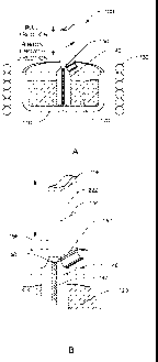
In the drawings, FIG. 1 is a diagram illustrating the crystal orientation of
an a-
plane single crystalline material;
FIG. 2 is a diagram illustrating the crystal orientation of a C-plane single
crystalline material;
FIG. 3A is a cross-sectional diagram of an embodiment of a single crystal
growth
apparatus;
FIG. 3B is an enlarged view of a portion of the apparatus of FIG. 3A;
FIG. 4 is another cross-sectional diagram of an embodiment of a single crystal
growth apparatus;
FIG. 5 is a cross-sectional diagram of an embodiment of a growth apparatus for
the production of C-plane single crystal sapphire;
FIG. 6 provides a photocopy of an X-ray topograph of C-plane ribbons
exhibiting
high polycrystallinity;
FIG. 7 provides a photocopy of an X-ray topograph of C-plane single crystal
sapphire ribbons of one embodiment exhibiting low polycrystallinity;
FIG. 8 is a photocopy of an X-ray topograph of a 10 cm diameter C-plane wafer
formed from a plate produced using the method described herein;
FIG. 9 is a photocopy of an X-ray topograph of a 5 cm C-plane wafer produced
using the Czochralski technique;
FIG. 10 is a photocopy of an X-ray topograph of a 5 cm C-plane wafer produced
using the Kyropoulos technique;
FIG. 11 is a photocopy of an X-ray topograph of a 5 cm C-plane wafer produced
using the heat exchanger method;
3
CA 02663382 2009-03-12
WO 2008/036888 PCT/US2007/079149
FIG. 12 is a photocopy of an X-ray topograph of a 5 cm C-plane wafer produced
using a traditional EFG technique; and
FIG. 13 is a photocopy of an X-ray topograph of a 10 cm x 30 cm C-plane ribbon
produced using the method described herein.
DETAILED DESCRIPTION
The materials and methods described in this disclosure include C-plane single
crystal sapphire and methods and apparatuses for producing C-plane sapphire. C-
plane
sapphire may be preferred to other crystal orientations due to its physical,
chemical,
mechanical and optical properties. For instance, C-plane sapphire wafers may
be
preferred in optical applications due to the absence of natural
crystallographic
birefringence. C-plane sapphire ribbons, or sheets, can be grown using, for
example,
shaped crystal growth techniques such as edge defined film-fed growth methods.
The
growth apparatus may include regions exhibiting different thermal gradients.
These
regions may provide different ribbon cooling rates at different times or
locations in the
production process or apparatus.
"Single Crystal Sapphire" means a-A1203, also known as corundum, that is
primarily single crystal.
"C-plane single crystal sapphire" refers to substantially planar single
crystal
sapphire, the c-axis of which is substantially normal (+/- 10 degrees) to the
major planar
surface of the material. Typically, the C-axis is less than about 1 degree
from the major
planar surface. See FIG. 2. The "sapphire C-plane" is as is known in the art
and is
typically the sapphire plane having a Miller index of 0001 and d spacing of
2.165
Angstroms.
"Dislocation" is used herein as it is used by those skilled in the art and
describes a
crystal defect that can be detected using X-ray diffraction topography based
on Bragg
diffraction.
"Thermal gradient" refers to the average change in temperature over distance
between two locations in a single crystal sapphire production apparatus. The
distance
between the two locations is measured on a line along which the single crystal
sapphire
advances during the production process. For example, in an edge defined film-
fed
4
CA 02663382 2009-03-12
WO 2008/036888 PCT/US2007/079149
growth technique, the temperature difference may be 50 degrees Celsius between
a first
position in the furnace and a second position in the furnace. Thermal gradient
units may
be, for example, "'degrees per cm" or "degrees per inch." If not specified,
the
temperature change is from a higher temperature to a lower temperature as the
sapphire
crystal passes from the first location to the second through the gradient.
"Ribbon" refers to a plate formed using a shaped crystal growth technique.
It has been shown that uniform a-plane sheets of single crystal sapphire can
be
produced efficiently using edge defined film-fed growth techniques (see U.S.
Patent
Application Publication 2005/0227117). However, C-plane sheets are typically
sliced
from a boule that is grown along different growth orientation using, for
example, the
Czochralski method. Boules can have various shapes and can be oriented so that
there
are different orientations of C-axis in different boules. For making wafers,
cylinders of
the desired diameters can be cored from boules and the desired wafers may be
cut from
the cylinders, for instance by using a wire saw slicing through the diameter
of the
cylinder. After cutting, the slice is typically ground and polished to produce
a C-plane
wafer. Wafer thicknesses may be chosen by first cutting the slice to a pre-
chosen width
and then lapping to the desired dimensions. Using this method of production to
form a
plate or wafer from a boule, each sheet or wafer must be cut along its major
planar
surface at least once. The extreme hardness of single crystal sapphire means
that the
cutting step may be expensive and time consuming. Additional preparation steps
may
also be required. Furthermore, the production of larger size wafers, e.g.,
greater than or
equal to 5 or 10 cm in diameter, may take weeks due to, in part, the secondary
and
tertiary operations. Adding an inch to the diameter of a wafer can double the
required
production time.
C-plane single crystal sapphire formed in sheets or ribbons could reduce or
shorten many of these preparation steps. For this reason and others, C-plane
sheets
exhibiting good optical characteristics and formed in sheets of appropriate
thickness
could provide a preferred source for C-plane single crystal sapphire.
Dislocations are typically undesirable in crystals and crystals with fewer
dislocations may be preferred. When a crystal wafer, such as a sapphire
crystal wafer, is
used as a substrate to grow other crystals such as GaN, a lower density of
dislocations in
5
I I J
CA 02663382 2011-04-07
the wafer may lead to a decreased number of dislocations in the GaN crystal.
It is also
believed that a large number of dislocations may lead to a break into
polycrystallinity.
Thus, a lower number of dislocations typically means a crystal of higher
quality.
Dislocation density may be determined by counting the number of individual
hairline dislocations apparent in an X-ray topograph of a specific crystal and
dividing the
total number of dislocations by the surface area of the crystal. For example,
the 10 cm
diameter circular wafer shown in FIG. 10 reveals approximately 80,000
dislocations
meaning a dislocation density of about 1000 dislocations per cm2.
Shaped crystal growth techniques such as edge defined film-fed growth methods
can be used to grow large sheets of single crystal sapphire. For instance, see
commonly
owned United States Patent Application Publication Number 2005/0227117. A
cross-
sectional view of an edge defined film-fed growth apparatus is provided in
FIG. 3A.
Crystal growth apparatus 100 includes crucible 110 that may contain melt 120.
The
temperature of the crucible may be raised and maintained above the melting
temperature
of the melt by induction heating coil 130. Melt can be drawn through capillary
feed die
140 in an upward direction to form a crystal at melt interface 150, at the top
of the die. As
the ribbon is pulled upwards, growth proceeds vertically until the ribbon is
of a desired
length. Although ribbon growth is discussed herein, the methods and apparatus
may be
equally applicable to tubes and/or other shapes.
Using edge defined film-fed growth techniques large sheets may be grown with
the thickness of the sheet being determined by, in part, the geometry of the
die that is
used. These sheets are typically "a-plane" sheets, i.e., the a axis is normal
to the major
planar surface. For example, see FIG. 1. In contrast, many of the methods
described
herein are directed to the formation of "C -plane" sheets, tubes or ribbons,
as illustrated in
FIG. 2. A visual comparison of the figures shows that the difference between
the plates of
FIG. 1 and FIG. 2 is that the crystal orientation has been rotated
approximately 90
degrees to render the C axis normal to the major plane (surface of greatest
area) of the
sheet. The width of the sheet is indicated by "x," the length by "y," and the
thickness by
"z." In both FIGS. 1 and 2, the in axis of the crystal is in substantially the
same direction
as is the central vertical y axis of the sheet, although it could be rotated.
For instance, the
6
CA 02663382 2009-03-12
WO 2008/036888 PCT/US2007/079149
crystal could be rotated around the C-axis so that the a and in axes change
positions.
Intermediate orientations known to those of skill in the art may also occur.
The crystal orientation of a single crystal material can often be fixed by the
placement of a seed crystal at the melt interface, for example, at the upper
surface of a
capillary feed die. The seed may be of sapphire or other material. The single
crystal
material formed from the melt typically crystallizes in an orientation that is
in alignment
with that of the seed. Thus, to form C-plane sheets instead of a-plane sheets,
the seed
may be rotated 90 degrees about its vertical axis from the a-plane position.
As the single
crystal material is formed, its crystal orientation may align with that of the
seed to
produce a single crystal sheet having a C-plane orientation.
Attempts at producing C-plane single crystal sapphire by edge defined film-fed
growth techniques were made by rotating the seed 90 degrees from the a-plane
position
and drawing the melt under conditions that have been successful in producing a-
plane
material. Results using these known techniques were unsatisfactory with
significant
polycrystallization resulting in a product that may not be useable in many
applications.
C-plane material has unique properties, one or more of which may explain why
it cannot
be produced using these methods. For example, compared to other orientations,
C-plane
material may have a unique singular crystallographic face. Compared to other
single
crystal sapphire orientations, C-plane material may have maximal surface
density, high
free surface energy, different thermal conductivity and a different growth
speed. One or
more of these properties may result in crystal growth behavior that is
different from that
of a-plane and/or other crystal orientations.
It has been found that high quality C-plane single crystal sapphire ribbons
can be
successfully made using an edge defined film-fed growth technique. Successful
techniques may include, for example, using different thermal gradients at
different points
in the edge defined film fed growth apparatus. For example, the crystal growth
apparatus
may include a first region having a first thermal gradient and a second region
having a
second thermal gradient. In some embodiments the second thermal gradient may
be
positioned later in the production process and may be of a lower value than
the first
thermal gradient. An apparatus may include one, two, three or more distinct
thermal
gradient regions.
7
CA 02663382 2009-03-12
WO 2008/036888 PCT/US2007/079149
In some embodiments, single crystal sapphire exhibiting little or no
polycrystallinity can be produced by subjecting the crystal to a higher rate
of cooling
immediately after formation from a melt and subsequently reducing the rate of
cooling as
the crystal advances through the production process. The rate of cooling may
be
controlled, at least partially, by the thermal gradient in the apparatus
and/or by the rate of
growth of the crystal. Once the material has cooled to below the brittle-
ductile transition
point it may be subjected to an uncontrolled rate of cooling although some
control may
still be desirable.
FIG. 3B provides an enlarged view of the central portion of the cross-
sectional
view of the apparatus of FIG. 3A. This detailed view shows die 140 including
capillary
channel 142 and melt interface 150 (at the die opening). Single crystal
sapphire ribbon
222 may be pulled upwardly from melt interface 150 where crystallization
begins to
occur. Centerline 156 cuts through the central axis of ribbon 222 as well as
die 140.
Thus, the cutaway view of FIG. 3B reveals approximately one half of the ribbon
and the
die.
Dashed line 152 depicts the level of a melt interface. Dashed lines 154 and
156
depict different points on ribbon 222 that are positioned at different
heights. As the
ribbon is drawn upwardly, new material crystallizes at or adjacent to melt
interface 152
and advances upwardly as the ribbon grows in length. As a portion of the
ribbon
advances from melt interface 152 to level 154 or to level 156 it maybe cooled
as it passes
from a position of higher temperature (152) to a position of lower temperature
(154). The
rate of cooling of the ribbon may be dependent, in part, on both the
temperature
difference between the two positions as well as the speed at which the ribbon
advances
between the positions in an apparatus. The thermal gradient measured over the
distance
between two positions, for example 152 and 154, may be greater than 1 C /cm,
greater
than 2 C /cm, greater than 3 C /cm, greater than 5 C /cm, greater than 10
C /cm,
greater than 20 C /cm, greater than 50 C /cm, greater than 100 C /cm,
greater than 200
C /cm, greater than 500 C /cm or greater than 1000 C /cm and may be
dependent, at
least partially, on the distance between 152 and 154. The rate of cooling will
also vary
with the rate of growth of the ribbon as a ribbon drawn at a faster rate will
reach a region
of lower temperature in a shorter period of time.
8
CA 02663382 2009-03-12
WO 2008/036888 PCT/US2007/079149
The thermal gradient between positions 154 and 156 may be greater than, less
than, or equal to the thermal gradient between 152 and 154. One, two, three or
more
different thermal gradients may be present in a single furnace or during a
single
production run.
At temperatures above about 1850 C it has been determined that control of the
cooling rate of a sapphire crystal may affect its crystalline quality. For
example, if
cooled too quickly, "slip" of one crystal plane over another may occur.
Another type of
crystalline defect that may be controlled by regulated cooling is
dislocations. Once the
temperature of the crystal drops below about 1850 C it may be of a more
stable single
crystal structure and the rate of cooling may not need to be regulated as
carefully. For
instance, if the crystal exits the apparatus below its brittle-ductile
transition point, it may
be allowed to cool to room temperature at a rapid rate without any
irreversible damage to
the crystal.
Thermal gradients may be varied at any specific location in the apparatus
although once ribbon production has started it may be preferred that gradients
are
maintained at constant values. However, gradients may be adjusted during
production to
compensate for variations in process parameters or to improve ribbon quality.
Thermal
gradients may be controlled by, for example, lowering or raising heat shields,
adding or
removing insulation, and/or actively heating or cooling a portion or portions
of the
apparatus.
Thermal gradients may be substantially constant over the length of the
gradient.
For instance, a thermal gradient may be substantially constant over a distance
of less than
1 cm, greater than 1 cm, greater than 2 cm, greater than 3 cm, greater than 5
cm, greater
than 10 cm, greater than 15 cm or greater than 20 cm. Thermal gradients may
also vary
over the length of the gradient, particularly at the beginning and/or end of
the gradient.
Of course, when moving from one gradient to another there may be a transition
distance
over which the gradient will shift from the first to the second gradient.
Unless otherwise
specified, a thermal gradient for a specific region is the average thermal
gradient
throughout the region.
A crystal plate may be formed using a shaped crystal growth technique and in
many of these methods, such as edge defined film-fed growth techniques, as the
crystal
9
CA 02663382 2009-03-12
WO 2008/036888 PCT/US2007/079149
lengthens, any point on the crystal advances directionally through the
apparatus. As the
point moves through the apparatus it may dwell for different amounts of time
in regions
exhibiting different thermal gradients. Depending on, for instance, the speed
of growth
and the length of the region, the dwell time for a point in a specific thermal
gradient may
be, for example, greater than 1 minute, greater than 5 minutes, greater than
10 minutes,
greater than 30 minutes, greater than 1 hour, greater than 2 hours or greater
than 3 hours.
In some embodiments, the thermal gradient at a point near the melt interface
may
be greater than the thermal gradient at a cooling region (a point above or
distal from the
melt interface). For example, referring to FIG. 3B, if the distance between
position 152
and position 154 is about 2.5 cm, the thermal gradient between 152 (at the
melt interface)
and 154 (thermal gradient 1) may be greater than or equal to 20 C/cm while a
second
thermal gradient (thermal gradient 2) between position 154 and position 156
(cooling
region) may be less than or equal to 10 C/cm. In some embodiments, thermal
gradient 1
may be greater than thermal gradient 2 and may be greater by a factor of more
than 1.1,
1.5, 2, 3, 5 or 10. In other embodiments, thermal gradient 1 may be greater
than thermal
gradient 2 by more than 2 C/cm, more than 5 C/cm, more than 10 C/cm, more
than 15
C/cm, or more than 20 C/cm. Depending on the specific apparatus and process
parameters such as the draw rate, thermal gradient 1 (from 152 to 154) may
exist over a
distance of, for example, greater than or equal to 1 cm, greater than or equal
to 2 cm,
greater than or equal to 3 cm, greater than or equal to 4 cm, greater than or
equal to 5 cm,
greater than or equal to 10 cm or greater than or equal to 20 cm. Thermal
gradient 2
(from 154 to 156) may exist over a distance of, for example, greater than or
equal to 1
cm, greater than or equal to 2 cm, greater than or equal to 3 cm, greater than
or equal to 4
cm, greater than or equal to 5 cm, greater than or equal to 10 cm, greater
than or equal to
20 or greater than or equal to 30 cm. In these and other embodiments, a
specific thermal
gradient may exist over a distance of less than or equal to 20 cm, less than
or equal to 110
cm, less than or equal to 5 cm, less than or equal to 3 cm or less than or
equal to 1 cm.
Typical draw rates may be, for example, less than 1 cm/hr, 1 cm/hr, 2 cm/hr, 3
cm/hr, 4 cm/hr, 5 cm/hr, 6 cm/hr or more. As draw rates increase, the dwell
time in each
thermal gradient region decreases. Thus, to subject a ribbon to similar
cooling
CA 02663382 2009-03-12
WO 2008/036888 PCT/US2007/079149
conditions, an increase in draw rate may be accompanied by an extended thermal
gradient
region.
FIG. 4 illustrates, in cross-section, a crystal growth apparatus similar to
that
shown in FIG. 3A except that it includes three dies to produce three ribbons
in parallel.
Included in the apparatus of FIG. 4 are horizontal heat shields 160 that can
be adjusted to
maintain a relatively constant rate of cooling and maintenance of the thermal
gradient as
described in U.S. Patent Application Publication 2005/0227 1 1 7. Also
included is
insulation layer 170 that may help to retain heat.
FIG. 5 illustrates one embodiment of a crystal growth apparatus that may be
used
to produce C-plane single crystal material. The figure provides a cutaway view
from one
end of apparatus 200, with 3 ribbons 222 being formed vertically. A ribbon is
formed in
a "downstream" direction, typically cooling as it progresses downstream. In
the
embodiment of FIG. 5, downstream is the upward vertical direction. The major
plane of
the ribbons, in this case the C-plane, is facing to the left and right in the
figure and the
view is from along an edge of each ribbon, revealing the ribbon thickness.
Crystal
growth apparatus 200 may include any or all of the components of crystal
growth
apparatus 100 such as horizontal heat shields 260 and insulation layer 272.
The
apparatus may include a melt source such as a melt fixture. In the illustrated
embodiment, the melt fixture may be a crucible 210. Crucible 210 can be
designed to
hold melt 220 which may be, for example, molten A1203. Crucible 210 may be
made of
any material capable of containing the melt. Suitable materials may include,
for example,
iridium, molybdenum, tungsten or molybdenum/tungsten alloys.
Molybdenum/tungsten
alloys may vary in composition from 0 to 100 % molybdenum.
Die 224 may be in fluid communication with crucible 210 and may be made of
any appropriate material. Materials may be identical or similar to those used
for the
crucible. The die may be used to form 1, 2, 3, 4, 5, 6, 7, 8, 9, 10 or more
ribbons
concurrently. For each ribbon to be formed, the die may include a cavity
dimensioned to
draw melt upwardly from the crucible to die opening 226 via capillary action.
Die
opening 226 can be dimensioned to match the desired width and depth dimensions
of the
ribbon to be drawn. For instance, the die opening may have a width of 5, 7.5,
10, 13, 15
or more cm and a depth of less than 0.1, 0.1, 0.2, 0.5 or 1.0 centimeters, or
greater. The
11
CA 02663382 2009-03-12
WO 2008/036888 PCT/US2007/079149
length of the ribbon may be determined by the length of the draw. Ribbons may
be
drawn, for example, to lengths of greater than or equal to 10 cm, 20 cm, 30
cm, 50 cm,
100 cm, 150 cm, or 200 cm.
Crystal growth apparatus 200 may also include afterheater 276 that may retain
heat, reduce the rate of cooling or increase the temperature in the space
containing the
ribbon or ribbons downstream of the melt interface. Afterheater 276 may be
positioned
so that it can supply heat to a portion of the apparatus that is downstream of
the melt
interface (die opening 226) by a distance of greater than or equal to 1 cm,
greater than or
equal to 2 cm, greater than or equal to 3 cm, greater than or equal to 5 cm,
or greater than
or equal to 10 cm. Afterheater 276 may reduce the thermal gradient in the
region in
which it is effective, for example, in thermal gradient zone Z2. During
operation,
afterheater 276 may provide heat to a portion of the apparatus that contains
crystallized
sapphire that is downstream of the melt interface. The heater may be, for
example, an
electrical resistance heater or an inductively coupled heater. Afterheater 276
may be used
to vary the thermal gradient and may form a thermal gradient zone (Z2) that
may be
adjacent to, but distinct from, a melt interface region (Z1) at the die
opening 226 of the
apparatus. The afterheater may be sized appropriately for the crystals being
produced.
The afterheater may be, for example, square, rectangular or composed of non-
continuous
plates. The afterheater may include, for example, a container 270 composed of
molybdenum and/or an alloy of molybdenum and may also include inductive
heating coil
232. Inductive heating coil 232 can be inductively coupled to enclosure 270 to
heat the
enclosure and the area containing the sapphire ribbon. Afterheater 276 may be
similar or
identical to heater 230 that is used to heat the lower portion of the
apparatus including,
for example, the crucible and the die. These two heaters may be controlled by
a common
controller or may be controlled independently of each other. Each of the
heaters may
supply a different energy flux to different portions of the apparatus
resulting in different
temperatures and thus different temperature gradients in different regions.
Other factors,
for example materials of composition, insulation and surface area, may also
affect
temperature and thermal gradient. The heaters may be spaced appropriately for
heating
(or reducing heat loss) different regions of the apparatus and may be, for
example, greater
12
CA 02663382 2009-03-12
WO 2008/036888 PCT/US2007/079149
than 1 cm, greater than 2 cm, greater than 5 cm, greater than 10 cm or greater
than 20 cm
apart from each other.
Insulating shield 272 may aid in reducing heat loss and can be made of a
material
capable of withstanding high temperature while also providing insulating
value. When
the apparatus includes an induction coil, the insulating shield may be of a
material that
does not couple with the induction coil. In other cases, the shield may
partially couple to
the electric field and may also provide an additional source of heat. For
instance, in some
embodiments, shields may be formed from graphite. Insulating shield 272 and/or
afterheater 276 may be useful in altering a thermal gradient or gradients that
provide for
the formation of C-plane single crystal sapphire having an absence of
polycrystallinity.
In some embodiments, the thermal gradient may be greater in the region of the
melt interface than it is above the melt interface. In this manner, a portion
of a sapphire
ribbon may cool at a faster rate immediately after formation at the die than
when it later
passes through the afterheater portion. Thus, a specific point on a ribbon may
be cooled
at a higher rate when first crystallized and then at a lower rate as the same
point on the
ribbon rises through the afterheater zone. At some locations, the thermal
gradient may be
zero which may result in a constant rate of heat loss in the ribbon throughout
the gradient.
By cooling a ribbon more quickly at the point of crystallization (near the
melt
interface) and less quickly at a point, for example, 5 cm, 10 cm, 15 cm, 20 cm
or more
above the die opening, dislocations and/or polycrystallization in the material
may be
significantly reduced or eliminated. In some embodiments, C-plane single
crystal
sapphire ribbons may contain fewer than 500 dislocations/cm2, fewer than 250
dislocations/cm2, fewer than 100 dislocations/em2, fewer than 10
dislocations/cm2or even
fewer than one dislocation/cm2 when determined by XRT.
In one embodiment, illustrated in FIG. 5, C-plane single crystal sapphire
production may be started by preparing an alumina melt in crucible 220.
Material may be
fed to the crucible prior to production or may be fed constantly or
intermittently during
production. Once the melt achieves temperature it can flow, via capillary
action, up
through cavities in die 224 (more easily seen in FIG. 3) to die opening 226.
The die
shown in FIG. 5 includes three cavities and three associated die openings for
concurrently
producing three C-plane single crystal sapphire ribbons. A die of any
practical number of
13
CA 02663382 2009-03-12
WO 2008/036888 PCT/US2007/079149
cavities may be used. A seed crystal, with its c-axis aligned from right to
left according
to FIG. 5, is placed in contact with the melt at the melt interface in the hot
zone. As the
seed is drawn vertically upward (downstream) cooling begins and the melt may
start to
crystallize around the seed in a crystalline orientation that matches that of
the seed. The
drawing process may proceed initially at a rate of about 1 to 15 cm/hr and,
after a neck is
formed, the rate may be maintained constant or may be changed to a different
rate. After
neck formation, the spread may grow and the temperature in the apparatus may
be
increased during this period. Once the width of the ribbon equals the width of
die opening
226, the ribbon can be drawn at a width and thickness that are determined by
the
dimensions of die opening 226. Drawing may continue to extend the ribbon to a
desired
length.
In some embodiments, once a point on the sapphire ribbon passes beyond region
Z1, the thermal gradient may be reduced. This can reduce the rate of cooling
and may
help to limit polycrystallinity. Region Z2 may include additional insulation
and/or an
additional heater such as an inductively coupled heater or resistive heater.
As the
sapphire ribbon grows, any point on the sapphire ribbon may pass from a region
having a
high thermal gradient (Z 1) to another region exhibiting a lower thermal
gradient (Z2).
Two or three different areas in substantially vertical or sequential alignment
(that may
include a crucible, for example) may exhibit different thermal gradients with
an upper
thermal gradient region providing less heat loss than a lower thermal gradient
region. For
example, zone ZI may exhibit a thermal gradient of 20 C/cm and Z2 may have a
gradient of 4 C/cm. Zone ZO in the crucible region may exhibit a thermal
gradient of
zero or close to zero, providing for a substantially constant temperature
throughout the
melt and the die. Thermal gradients may be varied with different rates at
which the
crystal is grown. For instance, for growth at a rate of from about 2 cm/hr to
about 5
cm/hr the temperature gradient at Zi may be, for example, between about 20 to
60
C/cm. The temperature gradient at Z2 may be, for example, from about 3 to 15
C/cm
and preferably about 8 to 10 C/cm.
Temperature gradient may also be affected by gas flow through the apparatus.
For instance, an inert gas such as argon may be flowed upwardly through the
apparatus
along the sapphire ribbon as it is being formed. It has been found that a flow
rate of
14
CA 02663382 2009-03-12
WO 2008/036888 PCT/US2007/079149
about 20 scfh can be used to help achieve the desired temperature gradients.
Control of
this flow rate may provide another method for adjusting the temperature
gradient.
Of course, additional downstream regions (cooler regions) may exhibit other
gradients to allow the material to cool to room temperature or closer to room
temperature
at the end of production. For example, a point on a ribbon may pass from a
region
exhibiting a high thermal gradient (region A) to a region of low thermal
gradient (region
B) and, optionally, to a third region (region C) having a high thermal
gradient. When
comparing thermal gradients of these regions, B may be less than A and B may
be less
than C. A may be less than or equal to or greater than C.
Using the methods described herein, ribbons, or plates, of C-plane single
crystal
sapphire have been produced in lengths of greater than 10 cm, greater than 20
cm, greater
than 30 cm and greater than 50 cm. Ribbons have been grown at widths of 15 and
20 cm
resulting in the capability of producing C-plane ribbons having surface areas
of about 1
m2. Circular wafers of up to 20 cm in diameter can be produced from these
plates. These
ribbons, plates and resulting wafers can contain fewer than 1000
dislocations/cm2, fewer
than 100 dislocations/cm2 or fewer than 10 dislocations/cm2.
EXAMPLES
Five centimeter width and ten centimeter width C-plane single crystal sapphire
ribbons were produced using two different embodiments of apparatuses and
methods. In
the first example, the apparatus exhibited a substantially constant thermal
gradient above
the melt interface. In the second, an apparatus that exhibited a greater
thermal gradient
(than the first apparatus) in a first region (Z 1) and a lower thermal
gradient (than the first
apparatus) in a second region (Z2) was used.
Example 1
In a first example, a technique for producing C-plane single crystal sapphire
plate
was attempted using apparatus and conditions known for producing a-plane
material. In
the apparatus a molybdenum crucible was filled with a supply of alumina
adequate to
produce a 30 cm long ribbon having a width of 10 cm and a thickness of 0.15
cm. The
CA 02663382 2009-03-12
WO 2008/036888 PCT/US2007/079149
melt was maintained at about 2050 C by inductively coupled heating. The
apparatus
included a molybdenum die having three vertically oriented capillary ducts
that exited at
die openings, each of which had a width of 10 cm and a thickness of 0.15 cm. A
seed
crystal of sapphire was contacted with the melt at the die opening. The seed
crystal was
oriented with its c-axis normal to the major vertical plane of the die. The
seed was then
drawn upwardly at a rate of 2.5 cm/hr. The heat loss directly above the die
opening was
controlled by a low thermal gradient section of the apparatus including
insulation and
heat shields. As the ribbon was drawn higher, the thermal gradient increased,
allowing
the ribbon to cool at a faster rate as it achieved a higher position in the
apparatus. This
may be similar or identical to a technique used to produce a-plane single
crystal sapphire,
except for the seed orientation.
Example 2
In Example 2, a single crystal growth apparatus such as that shown in FIG. 5
was
used. It differed from the apparatus used in Example 1. For instance, an
afterheater
above the hot zone was used to form a region of a reduced thermal gradient.
The
afterheater including a molybdenum enclosure 270, a second induction heating
coil 232
and horizontal heat shields 260 spaced closer together than in the apparatus
of Example
1. In addition, the single crystal growth apparatus of Example 2 included
graphite
insulation 272 surrounding the hot zone to a height of about 15 cm. The
apparatus
included a molybdenum triple die and molybdenum crucible as in Example 1.
The crucible was charged with alumina and heated to 2050 C to provide the
melt.
The melt progressed upwardly to the die openings via capillary action. A seed
crystal of
sapphire was contacted with the melt at the die opening. The seed crystal was
oriented
with its C-axis normal to the major vertical plane of the die to crystallize a
C-plane
ribbon. The seed was then drawn upwardly at a rate of 2.5 cm/hr.
At zone Z 1, the ribbon was exposed to an area having a greater thermal
gradient
(more heat loss) than at an equivalent point in Example 1. At zone Z1, the
thermal
gradient was about 40 C/cm while at zone Z2 the ribbon was exposed to an area
having a
lower thermal gradient (less heat loss) than at an equivalent point in Example
1. At zone
Z2, the thermal gradient was about 10 C/cm. Ribbons were drawn to a length of
40 cm.
16
CA 02663382 2009-03-12
WO 2008/036888 PCT/US2007/079149
The C-plane products produced in both Example 1 and Example 2 were evaluated
by visually inspecting each ribbon and by examining the X-ray Transmission
(XRT)
results of each of the ribbons. XRT can provide an indication of the number of
dislocations in each sample and can identify polycrystallinity.
FIG. 6 is a photocopy of the XRT results of the material made using the
process
of Example 1. There are many dislocations and polycrystallinity is visible
about half way
down the ribbon.
FIG. 7 is a photocopy of the XRT results of C-plane single crystal sapphire
made
using the process of Example 2. Analysis of the XRT results shows fewer than
100
dislocations per square centimeter indicating a high quality 10 cm wide ribbon
of C-plane
single crystal sapphire. Post-growth annealing was not required. Ribbons
produced by
the method and apparatus of Example 2 may be used to produce 10 cm (100 mm) C-
plane
single crystal sapphire wafers that may be used, for example, as a substrate
for gallium
nitride epitaxial growth for the production of light emitting diodes or laser
diodes. The
ribbon may be grown to the appropriate thickness and circular wafers may be
formed by
core drilling through a single thickness of the ribbon and then grinding,
lapping and
polishing to typical wafer tolerances. In contrast, wafers formed from a boule
are
typically core drilled and then wire sawed and subsequently ground, lapped and
polished.
Thus., shaped growth techniques can eliminate the need for extensive wire
sawing.
FIGS. 8-13 provide a comparison between C-plane single crystals grown by the
method described herein and with those produced using known techniques. FIG. 8
provides an x-ray topograph of a 10 cm C-plane single crystal sapphire wafer
cut from a
plate grown using the technique of Example 2. An x-ray topograph of a plate
(10 cm by
cm) produced using the same technique and showing fewer than 10 dislocations
per
cm2 is provided in FIG. 13. In both of FIGS. 8 and 13 there are lines showing
surface
bubbles (these can be polished out) but very few, if any, of the hair like
features that
indicate dislocations. In contrast, the x-ray topography in FIGS. 9-12 each
show
numerous dislocations. FIGS. 9-12 each provide a photocopy of an x-ray
topograph of a
5 cm C-plane wafer produced by a known method. FIG. 9 is from a wafer produced
30 using the Czochralski method. Examination shows a dislocation density of
about 10,000
dislocations per cm2. FIG. 10 is a wafer made from a crystal using the
Kyropoulos
17
I I y
CA 02663382 2011-04-07
technique and shows a dislocation density of about 1000 dislocations per cm2.
FIG. 11 is
a wafer made from a crystal using the heat exchanger method and shows a
dislocation
density of about 1000 dislocations per cm2. FIG. 12 is a wafer made from a
crystal using
the EFG technique and shows a dislocation density of about 1000 dislocations
per cm2.
While several embodiments of the present invention have been described and
illustrated herein, those of ordinary skill in the art will readily envision a
variety of other
means and/or structures for performing the functions and/or obtaining the
results and/or
one or more of the advantages described herein, and each of such variations
and/or
modifications is deemed to be within the scope of the present invention. More
generally,
those skilled in the art will readily appreciate that all parameters,
dimensions, materials,
and configurations described herein are meant to be exemplary and that the
actual
parameters, dimensions, materials, and/or configurations will depend upon the
specific
application or applications for which the teachings of the present invention
is/are used.
Those skilled in the art will recognize, or be able to ascertain using no more
than routine
experimentation, many equivalents to the specific embodiments of the invention
described herein. It is, therefore, to be understood that the foregoing
embodiments are
presented by way of example only and that, within the scope of the appended
claims and
equivalents thereto, the invention may be practiced otherwise than as
specifically
described and claimed. The present invention is directed to each individual
feature,
system, article, material, kit, and/or method described herein. In addition,
any
combination of two or more such features, systems, articles, materials, kits,
and/or
methods, if such features, systems, articles, materials, kits, and/or methods
are not
mutually inconsistent, is included within the scope of the present invention.
All definitions, as defined and used herein, should be understood to control
over
dictionary definitions, and/or ordinary meanings of the defined terms.
The indefinite articles "a" and "an," as used herein in the specification and
in the
claims, unless clearly indicated to the contrary, should be understood to mean
"at least
one."
All references, patents and patent applications and publications that are
cited or
referred to in this application can be referenced for additional information.
18