Note: Descriptions are shown in the official language in which they were submitted.
CA 02663424 2009-03-13
WO 2008/040132 PCT/CH2007/000469
DESCRIPTION
TITLE
Key for SMT applications
TECHNICAL FIELD
The present invention relates to a key for intermittent
electrical contact-connection of at least two
conductors arranged on a printed circuit board to an
electrically conductive contact element, in particular
for fixing on the printed circuit board in the context
of SMT technology. In this case, the key has at least
one base arranged on the printed circuit board and also
a key head - which is movable relative to the printed
circuit board and the base - with the contact element,
wherein the key head is connected to the base by means
of at least one movable membrane, and wherein base and
membrane are composed of an insulating elastic
material. The present invention furthermore relates to
methods for producing such a key or arrangements of
such keys and uses of such keys.
PRIOR ART
Contact key switches are used for example for mobile
telephones, remote controls and also for applications
for example in vehicles, etc. They are normally based
on keys or arrangements of keys which are composed of a
rubber-like elastic material (normally silicone) and
which are arranged on a printed circuit board, and
wherein a contact element (for example a contact pellet
composed of metal or carbon) is arranged on the
underside of an actual key head, such that when this
key head is depressed, the contact element is pressed
onto the printed circuit board in such a way that
conductors arranged thereon are connected to one
CA 02663424 2009-03-13
WO 2008/040132 PCT/CH2007/000469
- 2 -
another. Constructions of this type are disclosed in
EP 0938111 for example.
Nowadays there are two fundamental solution approaches
for realizing such a keypad with an overlying plastic
cap.
The first solution involves silicone switching mats
having at least one switching dome, but in general
usually a plurality of switching domes on a mat. The
switching domes are actuated by means of the plastic
cap and yield a clearly defined force-displacement
characteristic curve (tactile feedback). When the
electrically conductive contact pellet touches the
printed circuit board, the contact is closed and the
switch is thus actuated. Switching mats are usually
placed onto the printed circuit board manually.
Backlighting of the plastic caps is effected by means
of LEDs (light emitting diode) applied on the printed
circuit board.
The second solution involves so-called tact switches.
Tact switches are individual switching domes which are
provided with one or more little feet which are
soldered on the printed circuit board. Mounting is
usually effected automatically by the SMT method
(surface mount technology). The tact switches available
nowadays are of complex construction and therefore very
expensive. Backlighting of the plastic caps is usually
effected by means of LEDs applied on the printed
circuit board, but more recent variants also already
have backlighting integrated in the tact switch. Only a
few force-displacement variants are usually available.
SUMMARY OF THE INVENTION
Accordingly, the invention is based on the object of
providing an improved key or an improved contact key
CA 02663424 2009-03-13
WO 2008/040132 PCT/CH2007/000469
- 3 -
switch. What is specifically involved, in particular,
is improving a key with tactile feedback for
intermittent electrical contact-connection of at least
two conductors arranged on a printed circuit board to
an electrically conductive contact element (e.g.
contact pellet, electrically conductive coating or
metal dome) . In this case, the key has at least one
base arranged on the printed circuit board and also a
key head - which is movable (normally lowerable)
relative to the printed circuit board and the base -
with the contact element or with an underlying contact
element in the form of a metal dome which ensures the
tactile feedback and the electrical contact. The key
head is connected to the base by means of at least one
movable membrane, and the base and the membrane are
composed of an insulating elastic material, e.g.
(transparent) silicone.
The improvement is now achieved, inter alia, by virtue
of the fact that the key additionally has at least one
soldering foot which is incorporated by the first end
thereof in the base in a positively locking manner and
by the second end of which, the exposed soldering
region, the key can be fixed on the printed circuit
board. In this case, "incorporated in a positively
locking manner" should be understood to mean that the
soldering foot is incorporated in the base in such a
way that it cannot be removed or withdrawn from the
base without use of force.
Consequently, the heart of the invention consists,
inter alia, in the possibility of the fixing of the
key, specifically the soldering feet, not being
subsequently fixed to the base (e.g. by adhesive
bonding or clamping) but rather being embedded by the
one unexposed end in the base substantially completely
and in a positively locking manner. In this case, the
positively locking connection is preferably reinforced
CA 02663424 2009-03-13
WO 2008/040132 PCT/CH2007/000469
- 4 -
by the fact that the non-exposed end is embodied in
such a way that it cannot be withdrawn from the base
without the latter being destroyed. This is possible,
for example, by virtue of the fact that, in the case of
strip-type embodiment of the soldering foot, steps,
angles, curvatures or undulations are provided in the
non-exposed end, or by virtue of the fact that the non-
exposed end is embodied not as a strip but rather to a
certain extent in T- or L-shaped fashion, such that it
is held in the base. The base is normally a
circumferential ring (round, oval or cornered,
including with rounded corners) composed of elastic
material, in an identical manner to the key head, and
the elastic material is normally silicone.
It is an aim of this invention, therefore, to provide a
switching dome which can be equipped automatically,
comprising the following properties (which occur
individually or in combination and are unique
particularly in their combination):
= highly cost-effective;
= automatic mounting by means of SMT, delivery on
rolls;
= smallest possible structural size;
= both with short stroke 0.2 mm-0.8 mm (metal dome)
and with long stroke 0.8 mm-3 mm (switching mat);
= large choice of force-displacement characteristic
curves (tailored to customer's requirement;
= with integrated LED for backlighting as an option.
In accordance with a first preferred embodiment, two
soldering feet are present which are arranged on
opposite sides of the key or respectively the base. The
key can thus be fixed optimally on the printed circuit
board, for example in a soldering operation.
Preferably, the base is embodied as an element which,
on the printed circuit board, runs around the position
CA 02663424 2009-03-13
WO 2008/040132 PCT/CH2007/000469
- 5 -
of the conductors to be contact-connected and from
which the at least one soldering foot projects
laterally. In other words, the soldering foot
preferably bears on the printed circuit board. The
soldering foot can have a planar soldering region
bearing on the printed circuit board and parallel
thereto. The soldering region is therefore to a certain
extent a strip which projects laterally from the base.
Such a strip typically has a width of 0.5-5 mm, in
particular preferably of 1-3 mm. This in the case of a
base having a height h in the range of 0.2-2 mm, in
particular in the range of 0.5-1.5 mm, and a width in
the range of the same order of magnitude.
In order to be able to ensure the positively locking
connection, the soldering foot preferably has a
vertical section which is arranged substantially
perpendicular to the plane of the printed circuit
board. Said section is preferably arranged completely
in the base and at the lower end of which the soldering
region is arranged.
In particular with regard to a stabilization of the
base it may be advantageous if a circumferential or
substantially circumferentially and at most sectionally
interrupted stiffening is arranged in the base, said
stiffening preferably being embodied in the form of a
perforated disk whose plane is arranged parallel to the
plane of the printed circuit board. The stiffening and
the soldering foot are connected to one another or are
formed in one piece. The unit composed of stiffening
and soldering foot is preferably produced as a stamped
and formed part made from a metallic material.
In accordance with a further preferred embodiment, a
soldering insert is incorporated in the base, said
soldering insert having a circumferential or
circumferentially and at most sectionally interrupted
CA 02663424 2009-03-13
WO 2008/040132 PCT/CH2007/000469
- 6 -
stiffening which is incorporated substantially
completely in the base and which is preferably embodied
in the form of a perforated disk whose plane is
arranged parallel to the plane of the printed circuit
board, at which stiffening there are arranged a
vertical section which is arranged substantially
perpendicular to the plane of the printed circuit board
and which is incorporated substantially completely in
the base, and, adjacent to said section, a planar
soldering region bearing on the printed circuit board
and parallel thereto. This soldering insert therefore
combines firstly the provision of the possibility of
the fixing (soldering feet) and also of the stiffening
of the base.
In accordance with a further preferred embodiment, the
key head is composed at least partly of transparent or
translucent material, and an illumination element, in
particular an LED, is furthermore preferably arranged
in the key head. The contact-connection of the
illumination element can be effected via at least two
soldering feet. In this case, the illumination element
is in particular preferably contact-connected to the
two soldering feet by means of two contact-connection
elements (flexible wire, flexible lug) which are
preferably incorporated in the membrane. The soldering
feet can thus be used for the fixing of the key and at
the same time for the driving of the illumination
element, which significantly simplifies the production
process of circuit arrangements. In order to be able to
drive the two poles of the illumination element
separately, it proves to be advantageous if a
substantially circumferential stiffening interrupted
only at two locations is arranged in the base, said
stiffening preferably being embodied in the form of a
perforated disk whose plane is arranged parallel to the
plane of the printed circuit board, and if the contact-
connection elements produce an electrical contact
CA 02663424 2009-03-13
WO 2008/040132 PCT/CH2007/000469
- 7 -
between the illumination element and the stiffening, by
virtue of the fact that the two poles are linked via
the two mutually separate regions of the stiffening. In
other words, one soldering foot with one region of the
stiffening and a first contact-connection element is
connected to the first connection of the illumination
element, and the other soldering foot with the other
region of the stiffening and the second contact-
connection element is connected to the second
connection of the illumination element. Thus, it is
particularly advantageous for example when two
oppositely arranged soldering feet are arranged, and,
at least during production, at least two intervening
(in the circumferential direction), likewise oppositely
arranged mounting connections are arranged, which
preferably have a separating gap, which lead to the
interruption of the stiffening into the two stated
regions having different polarities.
In the case of such a possibility for the connection of
an illumination element, it proves to be advantageous
if at least one indicator for the connecting direction
of the illumination element is arranged in and/or on
the key head (e.g. depression, coloration, etc.).
For the above applications comprising one (or more)
illumination element, it is necessary, of course, for
the soldering feet and a possibly present stiffening or
respectively the contact-connection elements to be
composed of an electrically conductive material or to
have electrically conductive tracks. They are
preferably composed of a (tin-plated) metal or of an
electrically conductive plastic, wherein soldering feet
and stiffening in the case of metal are in particular
preferably produced in one piece in a stamping and
forming process. The contact-connection elements can be
soldered (e.g. wire bonding) or crimped onto such a
soldering insert. Possible metallic materials are in
CA 02663424 2009-03-13
WO 2008/040132 PCT/CH2007/000469
- 8 -
particular bronze, CuFe3P (e.g. with nickel coating),
SAE 1008, etc.
Furthermore, the present invention relates to a
soldering insert for a key such as is described above,
wherein the soldering insert particularly preferably
has the features described above.
In addition, the present invention relates to a two-
(series) and/or three-dimensional (mat) arrangement of
keys of a design such as is described above, or of such
soldering inserts. In the case of the arrangement,
preferably the keys or respectively the soldering
inserts are connected to one another via the soldering
feet and/or the mounting connections and are preferably
separated into individual keys only shortly before the
mounting or before the introduction into a mounting
apparatus.
Moreover, the present invention relates to a method for
producing a key of the type described above or for
producing an arrangement such as has been described
above. The method is preferably characterized in that
the contact pellet and also the soldering feet or the
entire soldering inserts, and also if appropriate an
illumination element (preferably in already connected,
that is to say soldered-together, form) and if
appropriate contact-connection element(s), are
introduced in an injection mold or compression mold,
and in that insulating elastic material (silicone) is
subsequently injected and is at least partly solidified
in the mold.
Such a method is preferably characterized in that an
above-described arrangement of keys is produced and
these are subsequently separated from one another to
form single keys, in particular preferably along a
separating edge which leads to the formation of two
CA 02663424 2009-03-13
WO 2008/040132 PCT/CH2007/000469
- 9 -
sections of the stiffening which are electrically
isolated from one another.
Finally, the present invention relates to the use of
such a key for fixing on a printed circuit board in
particular with the aid of a soldering operation by
means of the soldering feet, in particular preferably
in the context of SMT technology.
Further preferred embodiments are described in the
dependent claims.
BRIEF EXPLANATION OF THE FIGURES
The invention will be explained in more detail below on
the basis of exemplary embodiments in connection with
the drawings, in which:
Figure 1 shows an SMT single key without an LED,
wherein a) illustrates a central section in a
direction perpendicular to the orientation of
the soldering feet, b) illustrates a view
from above, and c) illustrates a central
section in a direction parallel to the
orientation of the soldering feet;
Figure 2 shows an SMT single key with a long stroke
and a contact pellet and also wire bonding of
an LED, in illustrations analogous to those
in figure 1;
Figure 3 shows an SMT single key with a short stroke
and a metal dome and also SMT soldering of an
LED, in illustrations analogous to those in
figure 1;
Figure 4 shows a soldering insert (SMT solder pin),
wherein a) illustrates a central section in a
direction A-A, b) illustrates a view from
above, and c) illustrates a central section
in a direction B-B; and
CA 02663424 2009-03-13
WO 2008/040132 PCT/CH2007/000469
- 10 -
Figure 5 shows a series of such soldering inserts (SMT
solder pin array).
WAYS OF EMBODYING THE INVENTION
The SMT single key is produced by the same method as a
customary switching mat in a compression mold for
silicone elastomer. In the mold, firstly an
electrically conductive contact pellet is introduced,
and then a defined quantity of unvulcanized silicone.
Afterward, the mold is closed and the silicone is
vulcanized at approximately 170 C for approximately ten
minutes. The shaped switching dome is then removed from
the mold, deburred (along a defined tearing edge), and
subjected to subsequent heat treatment at 150 C for 2h.
The membrane of the switching dome, in combination with
the material properties of the silicone type and the
spacing of the contact pellet with respect to the base,
is designed in such a way that a desired force-
displacement curve results upon actuation (tactile
feedback).
A novel additional factor now is the SMT solder pin
with two little soldering feet. This is a stamped and
bent part which fulfils three functions:
a) metal area for enabling an SMT mounting on the
printed circuit board (PCB) . SMT is the customary
method for populating printed circuit boards in
large batches.
b) contact area for connecting the LED
c) circumferential stiffening of the base, such that
the silicone does not yield during actuation.
CA 02663424 2009-03-13
WO 2008/040132 PCT/CH2007/000469
- 11 -
The SMT solder pin is introduced into the open mold
after the contact pellet and is then completely
enclosed by the silicone during the vulcanization
(retention by positively locking connection). After the
vulcanization, the part is deburred. Since the silicone
does not adhere on metal, the region of the little
soldering feet is made free of silicone again in the
course of deburring. This is effected by means of
exactly positioned tearing edges along the material
overflow channels. Since introducing an individual SMT
solder pin is not very efficient, it is also possible
for a plurality of contiguous SMT solder pins in an
array to be introduced into a plurality of mold
cavities and then to be separated from one another
after the vulcanization by means of a small stamping
tool.
If the SMT solder pin is provided with a separating
gap, the two little soldering feet are electrically
isolated from one another by the stamping. This in turn
enables the connection of an electrical component, e.g.
an LED, between the two little soldering feet.
The LED for key backlighting is fixed on the SMT solder
pin. This can be done by soldering (SMT) onto flexible
lugs or else preferably by wire bonding. Wire bonding
has the advantage that the wire connection can be
adapted as desired to the membrane geometry and that
the wires are very flexible and therefore do not or
hardly impair the force-displacement curve of the key.
During the vulcanization, the transparent silicone then
simply flows around the LED together with the SMT
solder pin and they are thus integrated into the
component in a watertight manner. The light scattering
can be set by varying the key head surface quality and
also the material color.
CA 02663424 2009-03-13
WO 2008/040132 PCT/CH2007/000469
- 12 -
Finally, the part is subjected to subsequent heat
treatment in order to prevent silicone outgassing.
If the LED functions only in one direction, an arrow or
some other symbol for the connecting direction can be
fitted to the key head, e.g. by means of a
corresponding depression in the mold.
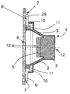
Figure 1 illustrates such a single key 1 in various
views. The single key or SMT single key 1 comprises a
key head 2 and also a circumferential base 4. A
likewise circumferential membrane 3 is arranged between
the base 4 and the key head 2. Base 4, membrane 3 and
key head 2 thus form the actual dome, and all three
elements are composed of silicone. A contact element 5,
for example a contact pellet 5 composed of metal or
conductive plastic, is arranged on the underside 12a of
the key head 2.
The tin-plated soldering feet 6 are then anchored in a
positively locking manner in the base 4. The soldering
region 28 of said soldering feet projects from the
base, and a vertical region 10 is completely embedded
in the base 4. Furthermore, there is arranged in the
base a stiffening 11, which in this case is embodied as
a perforated disk and which is embedded
circumferentially in the entire base.
Such a key 1 is fixed on the printed circuit board 8 by
means of two soldering locations 7. For dissipating
heat that possibly arises below the dome, it can be
advantageous if hot air can be led away or respectively
cool air can be fed in via venting channels in a
diagonal direction. However, the venting channels are
also crucial in order to permit the outflow of air upon
pressing and an intake of air upon release of the key
into the region below the key. If said venting channels
or corresponding means (holes in the membrane are also
CA 02663424 2009-03-13
WO 2008/040132 PCT/CH2007/000469-
- 13 -
conceivable) are not present, then the key, owing to
the air enclosed underneath, cannot be depressed or
respectively a key, once depressed, does not relax or
does so only very slowly.
Such a key normally has an overall height in the range
of 2-5 mm, preferably in the range of 3 to 4 mm. The
distance H between the printed circuit board 8 and the
underside of the contact pellet 5 is normally
approximately 1-2 mm, and opposite limbs of the base 4
have a distance k in the range of 3-8 mm, preferably in
the range of 4-5 mm. The key head 2 can be embodied in
round fashion and then has for example a diameter m in
the range of 2-4 mm. A contact pellet 5 is normally
embodied in circular or square fashion and has a
diameter 1 in the range of 2-3 mm. The soldering
regions 28 project at least 0.5 mm laterally beyond the
base, preferably in the range of 0.5 mm-2 mm.
The metal sheet from which the soldering feet and the
stiffening are produced (in one piece in a stamping and
forming method), normally has a thickness in the range
of 0.2-0.5 mm. The stiffening 11 is completely embedded
in the material of the base 4 and nowhere does it
emerge from the base 4. The vertical region 10 is
preferably likewise completely embedded in the base 4,
but can also be partly exposed downward with respect to
the printed circuit board, as can be discerned in
Figure 1.
Figure 2 illustrates an SMT single key with a long
stroke and a contact pellet and wire bonding of an LED.
An LED 13 is integrated in the key head 2. In this
case, the two soldering feet 6 serve for driving the
LED 13. For this purpose, the stiffening 11 is divided
into two regions having different polarities 21. The
LED 13 is connected via a first flexible wire 14 to the
region having a first polarity, and the second
CA 02663424 2009-03-13
WO 2008/040132 PCT/CH2007/000469
- 14 -
connection of the LED 13 is connected via a second
flexible wire 14 to the other region having a second
polarity. The connection between the flexible wire 14
and the stiffening and also between the flexible wire
14 and the LED 13 can be a gold-plated soldering
location for wire bonding. The two regions of the
stiffening 11 are electrically isolated from one
another by means of a separating gap 17. Figure 2 in
this case illustrates the situation directly after
production in which the two regions are still connected
to one another. Specifically, in order to simplify
production, the stiffening is initially presented with
two laterally linked mounting connections 19 which
likewise have a separating gap 17. Prior to the (final)
mounting, separation is effected at the separating edge
16 and the two arms 20a and 20b are thus severed and
the two regions of the stiffening 11 are therefore
electrically isolated from one another. The two regions
of the stiffening 11 are to be connected to
corresponding conductor tracks on the printed circuit
board separately from one another with the two opposite
soldering feet 6.
The distance between the underside of the mounting
connections 19 with respect to the printed circuit
board should be at least 0.2 mm (the interspace is
insulated by means of silicone) in order that a short
circuit with respect to the printed circuit board can
be avoided.
Since an LED normally has a predetermined connecting
direction, it proves to be advantageous if an indicator
18 is arranged on the key head, by way of example.
Figure 3 illustrates an SMT single key with a short
stroke and a metal dome and SMT soldering of an LED. In
this case, the membrane is a flat membrane 23, and the
key head 2 has on its underside an actuation plunger
CA 02663424 2009-03-13
WO 2008/040132 PCT/CH2007/000469
- 15 -
24, which acts on a metal dome 22. The LED arranged in
the key head 2 is connected to the two regions of the
stiffening via two flexible lugs 25. The two respective
connections of the flexible lugs can be provided by
means of SMT soldering locations 26.
Figure 4 illustrates an SMT solder pin, that is to say
a component which can be produced as a stamped and bent
part and can be introduced into a mold. It comprises
the stiffening 11, the soldering feet 6 and also the
mounting connections 19. It can be discerned in this
figure that the soldering feet 6 have a width p in the
range of 1-3 mm, and the mounting connections 19 have a
width likewise in the range of 1-3 mm. The distance
between the two arms 20a and 20b is preferably at least
0.5 mm. The stiffening is rounded in square fashion
(with a rounding R of approximately 0.5 mm) and has an
outer width of 5-7 mm.
Such solder pins or soldering inserts are
advantageously produced as an SMT solder pin array as
illustrated in figure 5, that is to say that the
individual soldering inserts are connected to one
another in a chain or even in a matrix via the mounting
connections 19 and/or the soldering feet 6. In this
case, the dimensions w, x, y can be 12, 48 and 60 mm,
respectively. These SMT solder pins can therefore be
arranged in a series or continuously (for example on a
roll). Stamping after vulcanization.
Specific embodiments:
Short stroke 0.2 mm - 0.8 mm (metal dome makes any
selectable force-displacement curve and electrical
contact)
CA 02663424 2009-03-13
WO 2008/040132 PCT/CH2007/000469
- 16 -
Long stroke 0.8 mm - 3 mm (silicone membrane makes any
selectable force-displacement curve, contact pellet
makes electrical contact)
With or without LED
Specific variants:
Contact pellet: all customary contact pellets can be
used such as carbon pellet, gold pellet, SC pellet or
else conductive lacquer. The choice of contact pellet
depends on the electrical requirements made of the
switching dome. The pellet diameter has to be adapted
to the size of the parts (e.g. 2.5 mm).
Metal dome: the metal dome can have a geometry such as
e.g. round or four-leg. The choice of metal dome
depends on the force-displacement requirements made of
the switching dome. The dome diameter has to be adapted
to the size of the parts (e.g. 5.0 mm).
The metal dome can be fitted to the lower base either
by adhesive bonding of the actuation plunger or by
means of a customary adhesive film, and this is
normally the last process step. It is likewise possible
for metal domes to be adhesively bonded fixedly to the
base by means of little fixing feet integrally formed
for this purpose. Manufacturers of such metal domes are
e.g. Nicomatic in Europe, Snaptron in USA or Truetone
in Asia, to name just a few.
Force-displacement curve; by designing the correct
membrane geometry or respectively the metal dome in
combination with the silicone properties, it is
possible to realize almost any desired curve according
to customer specifications.
CA 02663424 2009-03-13
WO 2008/040132 PCT/CH2007/000469
- 17 -
Component height: the key head can be configured with
any desired height.
LED: a commercially available LED can be used; all that
should be taken into consideration is the insulation
size and suitability for SMT soldering or wire bonding
(arrangement and quality of the soldering area). In
this case, color, brightness, emission angle, etc. can
be chosen from a wide range. Example: Kingbright chip
LED 0805, superbright with dimensions of 2 mm x 1.25 mm
x 1.1 mm. It is also conceivable to integrate a
possible series resistor.
LED fixing:
Wire bonding: a wire-bonder can be used to produce a
flexible connection between SMT solder pin and LED. In
this case, there are gold or aluminum wires with
different thicknesses. By way of example, gold wire
having a thickness in the range of 30 - 150 pm has
proved to be worthwhile, and in the case of gold wire a
thickness in the region of 100 pm has proved to be
particularly advantageous.
SMT soldering: in the case of the metal dome
embodiment, the LED can be soldered directly on the SMT
solder pin if the latter is provided with two flexible
lugs since here it is only necessary to overcome a
small stroke in a flat membrane.
SMT solder pin:
The SMT solder pin is designed as a stamped and bent
part, but a conductive plastic part is also possible
(3D-MID molded interconnect devices).
CA 02663424 2009-03-13
WO 2008/040132 PCT/CH2007/000469
- 18 -
Material is preferably CuFe3P with a 2}.zm thick nickel
coating (Ni), but can also be e.g. bronze or stainless
steel (SAE 1008).
The region of the little soldering feet is preferably
tin-plated (Sn) for lead-free SMT soldering onto the
printed circuit board without any problems.
The region for the wire bonding is ideally coated with
0.2 pm of gold (Au) for completely satisfactory
adhesion.
The SMT solder pin can be present as a single part or
contiguously in series as an array, e.g. with a
separating gap for electrical isolation.
Key head: transparent silicone or milky colored
silicone (diffusion of the light) Polished or rough
surface (diffusion of the light). In the case of a
polished surface, the silicone is clear like glass.
Production method:
The part is preferably produced by compression molding,
but it is also possible by transfer molding.
Fully automated liquid injection molding (LIM) with
liquid silicone rubber (LSR) is expedient in the case
of large numbers of items.
Advantages:
= very cost-effective since few components and
simple method;
= automatic placement by means of SMT, delivery on
rolls;
= with integrated LED for backlighting as an option;
CA 02663424 2009-03-13
WO 2008/040132 PCT/CH2007/000469
- 19 -
= LED integrated in key head brings light where it
is needed, and that is absolutely novel for a long
stroke;
= LED and key are mounted on printed circuit board
in one work operation, and that saves a mounting
operation;
= LED is protected against ambient influences;
= extremely small structural size;
= highly variable, customer-specific solution
possible in a simple manner;
= both with short stroke 0.2 mm-0.8 mm (metal dome)
and with long stroke 0.8 mm-3 mm (switching mat);
= large choice of force-displacement characteristic
curves (tailored to customer requirements);
= many contact pellets possible;
= one system for all requirements;
= no loose parts since SMT solder pin and LED are
embedded directly in the component;
= temperature range -40 C - +110 C
Applications (examples):
= as key/switch for any input device where a key is
actuated by means of a plastic cap;
= replaces present-day switching mats e.g. for input
devices in an automobile (window winding
mechanism, mirror adjuster, radio);
= replaces conventional tact switches since LED
identically integrated and by virtue of being
cheaper.
LIST OF REFERENCE SYMBOLS
1 Single key
2 Key head
3 Membrane
4 Base
5 Contact element, contact pellet
6 (Tin-plated) soldering foot
7 Soldering location
CA 02663424 2009-03-13
WO 2008/040132 PCT/CH2007/000469
- 20 -
8 Printed circuit board (PCB)
9 Venting channel
Vertical section of 6
11 (Circumferential) stiffening
5 12 Top side of 2
12a Underside of 2
13 LED
14 Flexible wire
Gold-plated soldering location
10 16 Separating edge
17 Separating gap
18 Indicator for connecting direction
19 Mounting connection
20a/b Arms of 19
15 21 Connection polarity
22 Metal dome
23 Flat membrane
24 Actuation plunger
Flexible lug
20 26 Soldering location
27 Soldering insert, solder pin
28 Soldering region
h Height of 4
H Distance between 5 and 8
25 k Distance between limbs of 4
1 Diameter/width of 5
m Diameter/width of 2
n Inner distance between limbs of 11
P Width of 6
q Outer distance between limbs of 11
R Radius
s Width of 19
t Width of 17
u Height of 10
v Thickness of 19
w,x,y Distances