Note: Descriptions are shown in the official language in which they were submitted.
CA 02663800 2015-01-16
WO 2008/036469 PCT/US2007/074795
TILE SUB-ARRAY AND PHASE ARRAY ANTENNA CIRCUITS AND TECHNIQUES
FIELD OF THE INVENTION
[0001] This invention relates generally to phased array antennas adapted
for volume
production at a relatively low cost and having a relatively low profile and
more particularly
to radio frequency (RF) circuits and techniques utilized in phased array
antennas.
BACKGROUND OF THE INVENTION
[0002] As is known in the art, a phased array antenna includes a plurality of
antenna
elements spaced apart from each other by known distances coupled through a
plurality of
phase shifter circuits to either or both of a transmitter or receiver. In some
cases, the
phase shifter circuits are considered to be part of the transmitter and/or
receiver.
[0003] As is also known, phased array antenna systems are adapted to produce a
beam
of radio frequency energy (RF) and direct such beam along a selected direction
by
controlling the phase (via the phase shifter circuitry) of the RF energy
passing between the
transmitter or receiver and the array of antenna elements. In an
electronically
scanned phased array, the phase of the phase shifter circuits (and thus the
beam direction)
is selected by sending a control signal or word to each of the phase shifter
sections. The
control word is typically a digital signal representative of a desired phase
shift, as well as
a desired attenuation level and other control data.
[0004] Including phase shifter circuits and amplitude control circuits in
a phased array
antenna typically results in the antenna being relatively large, heavy and
expensive. Size,
weight and cost issues in phased array antennas are further exacerbated when
the antenna
is provided as a so-called "active aperture" (or more simply "active") phased
array
antenna since an active aperture antenna includes both transmit and receive
circuits.
[0005] Phased array antennas are often used in both defense and commercial
electronic
systems. For example, Active, Electronically Scanned Arrays (AESAs) are in
demand
for a wide range of defense and commercial electronic systems such as radar
surveillance,
terrestrial and satellite communications, mobile telephony, navigation,
identification, and
electronic counter measures. Such systems are often used in radar for National
Missile
1
CA 02663800 2009-03-18
WO 2008/036469
PCT/US2007/074795
Defense, Theater Missile Defense, Ship Self-Defense and Area Defense, ship and
airborne radar systems and satellite communications systems. Thus, the systems
are
often deployed on a single structure such as a ship, aircraft, missile system,
missile
platform, satellite or building where a limited amount of space is available.
[0006] AFSAs offer numerous performance benefits over passive scanned arrays
as
well as mechanically steered apertures. However, the costs that can be
associated with
deploying AESAs can limit their use to specialized military systems. An order
of
magnitude reduction in array cost could enable widespread AESA insertion into
military
I 0 and commercial systems for radar, communication, and electronic warfare
(EW)
applications. The performance and reliability benefits of AESA architectures
could
extend to a variety of platforms, including ships, aircraft, satellites,
missiles, and
submarines.
[0007] Many conventional phased array antennas use a so-called "brick" type
architecture. In a brick architecture, radio frequency (RF) signals and power
signals fed
to active components in the phased array are generally distributed in a plane
that is
perpendicular to a plane coincident with (or defined by) the antenna aperture.
The
orthogonal arrangement of antenna aperture and RF signals of brick-type
architecture can
sometimes limit the antenna to a single polarization configuration. In
addition, brick-type
architectures can result in antennas that are quite large and heavy, thus
making difficult
transportability and deployment of such antennas.
[0008] Another architecture for phased array antennas is the so-called
"tile"
architecture. With a tile architecture, the -RE circuitry and signals are
distributed in a
plane that is parallel to a plane defined by the antenna aperture. The tile
architecture uses
basic building blocks in the form of "tiles" wherein each tile can be formed
of a multi-
layer printed circuit board structure including antenna elements and its
associated RF
circuitry encompassed in an assembly, and wherein each antenna tile can
operate by itself
as a substantially planar phased array or as a sub-array of a much larger
array antenna.
[0009] For an exemplary phased array having a tile architecture, each
tile can be a
highly integrated assembly that incorporates a radiator, a transmit/receive
(T/R) channel,
2
CA 02663800 2009-03-18
WO 2008/036469 PCT/US2007/074795
RF and power manifolds and control circuitry, all of which can he combined
into a low
cost light-weight assembly for implementing AESA. Such an architecture can be
particularly advantageous for applications where reduced weight and size of
the antenna
are important to perform the intended mission (e.g., airborne or space
applications) or to
transport and deploy a tactical antenna at a desired location.
[0010] It would, therefore, he desirable to provide an AESA having an order of
magnitude reduction in the size, weight, and cost of a front end active array
as compared
to existing technology, while simultaneously demonstrating high performance.
I 0
SUMMARY OF THE INVENTION
[0011] As mentioned above, the relatively high cost of phased arrays has
precluded the use
of phased arrays in all but the most specialized applications. Assembly and
component costs,
particularly for active transmit/receive channels, are major cost drivers.
Phased array costs
can be reduced by utilizing batch processing and minimizing touch labor of
components and
assemblies. It would he advantageous to provide a tile sub-array for an
Active,
Electronically Scanned Array (AESA) that is compact, which can be manufactured
in a cost-
effective manner, that can be assembled using an automated process, and that
can be
individually tested prior to assenibly into the AESA. There is also a need to
lower
acquisition and life cycle costs of phased arrays, while at the same time
improving
bandwidth, polarization diversity and robust RF performance characteristics to
meet
increasingly more challenging antenna performance requirements.
[0012] At least some embodiments of a tile sub-array architecture
described herein enable
a cost effective phased array solution .for a wide variety of phased array
radar missions or
communication missions for ground, sea and airborne platforms. In addition, in
at least one
embodiment, the tile sub-array provides a thin, lightweight construction that
can also be
applied to conformal arrays on an aircraft wing or fuselage or on a Unmanned
Aerial Vehicle
(UAV).
[0013] In one so-called "packageless T/R channel" embodiment, a tile sub-
array
simultaneously addresses cost and performance for next generation radar and
communication systems. Many phased array designs are optimized for a single
mission
3
CA 02663800 2009-03-18
WO 2008/036469
PCT/US2007/074795
or platform. In contrast, the flexibility of the tile sub-array architecture
described herein
enables a solution for a larger set of missions. For example, in one
embodiment, a so-
called upper multi-layer assembly (UMLA) and a lower multi-layer assembly
(LMLA),
each described further herein, serve as common building blocks. The UMLA is a
layered
RF transmission line assembly which performs RF signal distribution, impedance
matching and generation of polarization diverse signals. Fabrication is based
on multi-
layer printed wiring board (PWB) materials and processes. The LMLA integrates
a
package-less Transmit/ Receive (T/R) channel and an embedded circulator layer
sub-
assembly. In a preferred embodiment, the LMLA is bonded to the UMLA using a
ball
grid array (BGA) interconnect approach. The package-less T/R channel
eliminates
expensive T/R module package components and associated assembly costs. The key
building block of the package-less LMLA is a lower multi-layer board (LMLB).
The
LMLB integrates RF, DC and Logic signal distribution and an embedded
circulator layer.
All T/R channel monolithic microwave integrated circuits (MM IC's) and
components,
I 5 RF, DC/Logic connectors and thermal spreader interface plate can be
assembled onto the
LMLA using pick and place equipment.
[0014] In accordance with a further aspect of the present invention, a
tile sub-array
comprises at least one printed circuit board assembly comprising one or more
RF
interconnects between different circuit layers on different circuit board with
each of the
RF interconnects comprising one or more RF matching pads which provide a
mechanism
for matching impedance characteristics of RF stubs to provide the RF
interconnects
having desired insertion loss and impedance characteristics over a desired RF
operating
frequency band.
[00 I.5] With this particular arrangement, a tile sub-array can be
manufactured without
the need to perform any back-drill and back-fill operations typically required
to eliminate
RF via stubs. The RF matching pad technique refers to a technique in which a
conductor
is provided on blank layers (i.e., layers with no copper) of a circuit board
or in ground
plane layers (with etched relief area) of a circuit board. The conductor and
associated
relief area provided the mechanism to adjust impedance characteristics of RF
vias (also
referred to as RF interconnect circuits) provided in a circuit board. Since
the need to
utilize back-drill and back-fill operations is eliminated, the RF matching pad
approach
4
CA 02663800 2009-03-18
WO 2008/036469
PCT/US2007/074795
enables a standard, low aspect ratio drill and plate manufacturing operation
to produce an
RF via that connects inner circuit layers and which also has a low insertion
loss
characteristic across a desired frequency band such as X-Band GHz ¨ 12 GI-
1z).
[0016] As is known, mode suppression vias help electrically isolate the RF
interconnects from surrounding circuitry, thereby preventing signals from
"leaking"
between signal paths. In conventional systems, the mode suppression vias are
also drilled
and plated at the same time the interconnecting RF via is drilled and plated.
I 0 [0017] With the RF matchirv2, pad approach of the present
invention, however, all RE
and mode suppression vias can be drilled and plated through the entire
assembly and
there is no need to utilize and back drill and fill operations on the RE
interconnects.
Thus, manufacturirg costs associated with hack drill and back fill operations
can be
completely eliminated while simultaneously improving RF performance because
channel
to channel variations due to drill tolerances and backfill material tolerances
are
eliminated.
[0018] In One embodiment, the RF matching pad technique utilizes copper
disks
surrounded by an annular ring relief area in ground plane layers of RF
interconnects and
mode suppression circuits. The RE matching pad technique is a general
technique which
can be applied to any RE stub extending a quarter-wavelength, or less, beyond
an RF
junction between an RF interconnect and an RF signal path such as a center
conductor of
a stripline transmission line.
BRIEF DESCRIPTION OF THE DRAWINGS
[0019] The foregoing features of this invention, as well as the invention
itself, may be
more fully understood from the following description of the drawings in which:
[0020] FIG. 1 is a plan view of an array antenna formed form a plurality
of tile sub-
arrays;
[00211 FIG. I A is a perspective view of a tile sub-array of the type used
in the array
antenna shown in FIG. I;
[0022] FIG. 1B is an exploded perspective view of a portion of the tile
sub-array shown
in FIG. IA:
5
CA 02663800 2009-03-18
WO 2008/036469 PCT/US2007/074795
10023] FIG. 1C is a cross-sectional view of a portion of the tile sub-
array shown in
FIGs. IA and 1B.
[0024] FIG. 2 is a block diagram of a portion of a dual circular
polarized (CP) tile sub-
array having a single transmit/receive (T/R) channel;
[0025] FIG. 3 is a cross-sectional view of an upper multi-layer assembly
(UMLA) of
the type shown in FIG. IC;
[0026] FIG. 4 is an enlarged cross-sectional view of the transition shown
in FIG. 3;
[0027] FIG. 4A is a top view of the cross-section in FIG. 4
[0028] FIG. 43 is a bottom view of the cross-section in FIG. 4
I 0 10029] FIG. 4C is an enlarged perspective view of the RF transition
shown in FIG. 3;
[0030] FIG. 41) is a plot of predicted insertion loss vs. frequency for
the transition
shown in FIGs. 3 and 4;
[003 I] FIG. 5 is an enlarged cross-sectional view of the transition shown
in FIG. 3;
[0032] FIG. 5A is a top view of the cross-section in FIG. 5
IS [0033] FIG. 5B is a bottom view of the cross-section in FIG. 5
[0034] FIG. 5C is an enlarged perspective view of the transition shown in
FIG. 3;
[0035] FIG. 5D is a plot of predicted insertion loss vs. frequency for
the transition
shown in FIGs. 3 and 4;
[0036] FIG. 6 is a plan view of an exemplary geometry for a conductive region
or a
20 relief area of an RF matching pad;
[0037] FIG. 6A is a plan view of an exemplary geometry for a conductive region
or a
relief area of an RF matching pad; and
[0038] FIG. 7 is a block diagram of an alternate embodiment of a lower
multi-layer
assembly (LMLA) coupled to an upper multi-layer assembly (UMLA).
1003911 It should be understood that in an effort to promote clarity in
the drawings and the
text, the drawings are not necessarily to scale, emphasis instead is generally
placed upon
illustrating the principles of the invention.
11)0 DESCRIPTION OF THE PREFERRED EMBODIMENTS
[00401 Before describing the various embodiments of the invention, it
should be noted
that reference is sometimes made herein to an array antenna having a
particular array
shape and/or size (e.g., a particular number of antenna elements or a
particular number of
6
CA 02663800 2009-03-18
WO 2008/036469
PCT/US2007/074795
tiles) or to an array antenna comprised of a particular number of "tile sub-
arrays" (or
more simply "tiles"). One of ordinary skill in the art will appreciate that
the techniques
described herein are applicable to various sizes and shapes of array antennas.
[0041] Similarly, reference is sometimes made herein to tile sub-arrays having
a
particular geometric shape (e.g. square, rectangular, round) and/or size
(e.g., a particular
Humber of antenna elements) or a particular lattice type or spacing of antenna
elements.
One of ordinary skill in the art will appreciate that the techniques described
herein are
applicable to various sizes and shapes of array antennas as well as to various
sizes and
I 0 shapes of tile sub-arrays.
[0042] Thus, although the description provided herein below describes the
inventive
concepts in the context of an array antenna having a substantially square or
rectangular
shape and comprised of a plurality of tile sub-arrays having a substantially
square or
rectangular-shape, those of ordinary skill in the art will appreciate that the
concepts
equally apply to other sizes and shapes of array antennas and tile sub-arrays
having a
variety of different sizes. shapes, and types of antenna elements. Also, the
tiles may be
arranged in a variety of different lattice arrangements including, but not
limited to,
periodic lattice arrangements or configurations (e.g. rectangular, circular,
equilateral or
isosceles triangular and spiral configurations) as well as non-periodic or
other geometric
arrangements including arbitrarily shaped array geometries.
[0043] Reference is also sometimes made herein to the array antenna including
an
antenna element of a particular type, size and/or shape. For example, one type
of
radiating element is a so-called patch antenna element having a square shape
and a size
compatible with operation at a particular -frequency (e.g. 10 GHz) or range of
frequencies
(e.g. the X-band frequency range). Reference is also sometimes made herein to
a so-
called "stacked patch" antenna element. Those of ordinary skill in the art
will recognize,
of course, that other shapes and types of antenna elements (e.g. an antenna
element other
than a stacked patch antenna element) may also be used and that the size of
one or more
antenna elements may be selected for operation at any frequency in the RF
frequency
range (e.g. any -frequency in the range of about I GHz to about 100 GlAz). The
types of
radiating- elements which may be used in the antenna of the present invention
include but
7
CA 02663800 2009-03-18
WO 2008/036469
PCT/US2007/074795
are not limited to notch elements, dipoles, slots or any other antenna element
(regardless
of whether the element is a printed circuit element) known to those of
ordinary skill in the
art.
[0044] It should also be appreciated that the antenna elements in each tile
sub-array can
be provided having any one of a plurality of different antenna element lattice
arrangements including periodic lattice arrangements (or configurations) such
as
rectangular, square, triangular (e.g. equilateral or isosceles triangular),
and spiral
configurations as well as non-periodic or arbitrary lattice arrangements.
[0045] Applications of at least some embodiments of the tile array
architectures
described herein include, but are not limited to, radar, electronic warfare
(EW) and
communication systems for a wide variety of applications including ship based,
airborne,
missile and satellite applications. For at least one embodiment of the tile
sub-array, tile
sub-arrays having a weight of less than one (1) ounce per transmit/receive
(T/R) channel
and a production cost of less than $100 per channel are desired. It should
thus be
appreciated that the tile sub-array described herein can be used as part of a
radar system
or a communications system.
[0046] As will also be explained further herein, at least some embodiments of
the
invention are applicable, but not limited to, military, airborne, shipbome,
communications, unmanned aerial vehicles (UAV) and/or commercial wireless
applications.
[0047] The tile sub-arrays to be described hereinbelow can also utilize
embedded
circulators; a slot-coupled, polarized egg-crate radiator; a single integrated
monolithic
microwave integrated circuit (MMIC); and a passive radio frequency (RF)
circuit
architecture. For example, as described further herein, technology described
in the
.following commonly assigned United States Patents can be used in whole or in
part
and/or adapted to be used with at least some embodiments of the tile subarrays
described
herein: U.S. Patent no. 6,6 11,180, entitled "Embedded Planar Circulator";
U.S. Patent no.
6,624,787, entitled "Slot Coupled, Polarized, Egg-Crate Radiator"; and/or U.S.
Patent no.
6.731.189, entitled "Multilayer stripline radio frequency circuits and
interconnection
8
CA 02663800 2009-03-18
WO 2008/036469
PCT/US2007/074795
methods." Each of the above patents is hereby incorporated herein by reference
in their
entireties.
[0048] Referring now to FIG. 1, an array antenna 10 is comprised of a
plurality of tile
sub-arrays 12a ¨ I2x. It should be appreciated that in this exemplary
embodiment, x total
tile sub-arrays 12 comprise the entire array antenna 10. In one embodiment,
the total
number of tile sub-arrays is sixteen tile sub-arrays (i.e. x = 16). The
particular number of
tile sub-arrays 12 used to provide a complete array antenna can be selected in
accordance
with a variety of factors including, but not limited to, the frequency of
operation, array
gain, the space available for the array antenna and the particular application
for which the
array antenna 10 is intended to be used. Those of ordinary skill in the art
will appreciate
how to select the number of tile sub-arrays 12 to use in providing a complete
array
antenna.
10049] As illustrated in tiles I 2b and 12i, in the exemplary embodiment of
FIG. 1, each
tile sub-array I 2a ¨12x comprises eight rows 13a ¨ 13h of antenna elements 15
with each
row containing eight antenna elements 15 (or more simply, "elements 15"). Each
of the
tile sub-arrays 12a - I 2x is thus said to be an eight by eight (or 8x8) tile
sub-array. It
should be noted that each antenna element 15 is shown in phantom in FIG. 1
since the
elements 15 are not directly visible on the exposed surface (or front face) of
the array
antenna 10. Thus, in this particular embodiment, each tile sub-array I 2a ¨
12x comprises
sixty-four (64) antenna elements. In the case where the array 10 is comprised
of sixteen
(16) such tiles, the array 10 comprises a total of one-thousand and twenty-
four (1.024)
antenna elements IS.
'75
[0050] In another embodiment, each of the tile sub-arrays 12a-I2x
comprise 16
elements. Thus, in the case where the array 10 is comprised of sixteen (16)
such tiles and
each tiles comprises sixteen (16) elements 15, the array 10 comprises a total
of two-
hundred and fifty-six (256) antenna elements 15.
[0051] In still another exemplary embodiment, each of the tile sub-arrays
12a ¨ I 2x
comprises one-thousand and twenty-four (1024) elements 15. Thus, in the case
where the
array 10 is comprised of sixteen (16) such tiles, the array 10 comprises a
total of sixteen
9
CA 02663800 2009-03-18
WO 2008/036469
PCT/US2007/074795
thousand three-hundred and eighty-four (16,384) antenna elements 15.
[0052] In view of the above exemplary embodiments, it should thus be
appreciated that
each of the tile sub-arrays can include any desired number of elements. The
particular
number of elements to include in each of the tile sub-arrays 12a-12x can be
selected in
accordance with a variety of factors including but not limited to the desired
frequency of
operation, array gain, the space available for the antenna and the particular
application for
which the array antenna 10 is intended to be used and the size of each tile
sub-array 12.
For any given application, those of ordinary skill in the art will appreciate
how to select
an appropriate number of radiating elements to include in each tile sub-array.
The total
number of antenna elements 15 included in an antenna array such as antenna
array 10
depends upon the number of tiles included in the antenna array and as well as
the number
of antenna elements included in each tile.
[0053] As will become apparent from the description hereinbelow, each tile sub-
array
is electrically autonomous (excepting of course any mutual coupling which
occurs
between elements 15 within a tile and on different tiles). Thus, the RF feed
circuitry
which couples RF energy to and from each radiator on a tile is incorporated
entirely
within that tile (i.e. all of the RF feed and beamformina circuitry which
couples RF
signals to and from elements 15 in tile 12b are contained within tile 12b). As
will be
described in conjunction with FIGs. 1B and IC below, each tile includes one or
more RF
connectors and the RF signals are provided to the tile through the RF
connector(s)
provided on each tile sub-array.
[0054] Also, signal paths -for logic signals and signal paths for power
signals which
couple signals to and from transmit/receive (T/R) circuits are contained
within the tile in
which the T/R circuits exist. As will be described in conjunction with FIGs.
1B and IC
below, RF signals are provided to the tile through one or more power/ logic
connectors
provided on the tile sub-array.
[0055] The RF beam for the entire array I 0 is formed by an external
beamformer (i.e.
external to each of the tile subarrays 12) that combines the RF outputs from
each of the
tile sub-arrays 12a-12x. As is known to those of ordinary skill in the art,
the beamformer
I 0
CA 02663800 2009-03-18
WO 2008/036469 PCT/US2007/074795
may be conventionally implemented as a printed wiring board stripline circuit
that
combines N sub-arrays into one RF signal port (and hence the beamformer may be
referred to as a I :N beam former).
[0056] The tile sub-arrays are mechanically fastened or otherwise secured to a
mounting structure using conventional techniques such that the array lattice
pattern is
continuous across each tile which comprises the array antenna. In one
embodiment, the
mounting structure may be provided as a "picture frame" to which the tile-
subarrays are
secured using fasteners (such as #10-32 size screws, for example). The
tolerance
between interlocking sections of the tile is preferably in the range of about
+/-.005 in.
although larger tolerances may also be acceptable based upon a variety of
factors
including but not limited to the -frequency of operation. Preferably, the tile
sub-arrays
2a ¨ I 2x are mechanically mounted such that the array lattice pattern (which
is shown as
a triangular lattice pattern in exemplary embodiment of FIG. 1) appears
electrically
continuous across the entire surface 10a (or "thee") of the array 10.
[0057] It should be appreciated that the embodiments of the tile sub-
arrays described
herein (e.g. tile sub-arrays I 2a¨ I 2x) differ from conventional so-called
"brick" array
architectures in that the microwave circuits of the tile sub-arrays are
contained in circuit
layers which are disposed in planes that are parallel to a plane defined by a
face (or
surface) of an array antenna (e.g.. surface 10a of array antenna 10) made up
from the tiles.
In the exemplary embodiment of FIG. I, for example, the circuits provided on
the layers
of circuit boards from which the tiles I2a ¨I2x are provided are all parallel
to the surface
I Oa of array antenna 10. By utilizing circuit layers that are parallel to a
plane defined by
a face of an array antenna, the tile architecture approach results in an array
antenna
having a reduced profile (i.e. a thickness which is reduced compared with the
thickness of
conventional array amennas).
[0058] Advantageously, the tile sub-array embodiments described herein can be
manufactured using standard printed wiring board (PWB) manufacturing processes
to
produce highly integrated, passive RF circuits, using commercial, off-the-
shelf (COTS)
microwave materials, and highly integrated, active monolithic microwave
integrated
circuits (MM IC's). This results in reduced manufacturing costs. Array antenna
I I
CA 02663800 2009-03-18
WO 2008/036469
PCT/US2007/074795
manufacturing costs can also be reduced since the tile sub-arrays can be
provided from
relatively large panels or sheets of PWBs using conventional PWB
manufacturing.
techniques.
[00591 In one exemplary embodiment, an array antenna (also sometimes referred
to as
a panel array) having dimensions of 0.5 meter x 0.5 meter and comprising 1024
dual
circular polarized antenna elements was manufactured on one sheet (or one
multilayer
PWB). The techniques described herein allow standard printed wiring board
processes to
be used to thbricate panels having dimensions up to and including 1m x 1m with
up to
4096 antenna elements from one sheet of multi-layer printed wiring boards
(PWBs).
Fabrication of array antennas utilizing large panels reduces cost by
integrating many
antenna elements with the associated RF .feed and beamforming circuitry since
a "batch
processing" approach can be used throughout the manufacturing process
including
fabrication of T/R channels in the array. Batch processing refers to the use
of large
volume fabrication and/or assembly of materials and components using automated
equipment. The ability to use a batch processing approach for fabrication of a
particular
antenna design is desirable since it generally results in relatively low
fabrication costs.
Use of the tile architecture results in an array antenna having a reduced
profile and
weight compared with prior art arrays of the same size (i.e.. having
substantially the same
physical dimensions).
[0060] Referring now to FIG. IA in which like elements of FIG. I are
provided having
like reference designations, and taking tile sub-array 12b as representative
of tile sub-
arrays 12a and 12c-12x, the tile sub-array 12b includes an upper multi-layer
assembly
(UMLA) 18. The UN41_,A 18 includes a radiator subassembly 22 which, in this
exemplary
embodiment, is provided as a so-called "dual circular polarized stacked patch
egg-crate
radiator" assembly which may be the same as or similar to the type described
in U.S. Pat.
No. 6,624,787 B2 entitled "Slot Coupled, Polarized, Egg-Crate Radiator"
assigned to the
assignee of the present invention and hereby incorporated herein by reference
in its
entirety. It should, of course, be appreciated that a specific type of
radiator sub assembly
is herein described only to promote clarity in the description provided by the
drawings
and text. The description of a particular type of radiator is not intended to
be, and should
not be construed as, limiting in any way. Thus, antenna elements other than
stacked
12
CA 02663800 2009-03-18
WO 2008/036469
PCT/US2007/074795
patch antenna elements may be used in the tile sub-array.
[0061] The radiator subassembly 22 is provided having a first surface 22a
which can
act as a radome and having a second opposing surface 22b. As will be described
in detail
below in conjunction with FIGs. IB and IC, the radiator assembly 22 is
comprised of a
plurality of microwave circuit boards (also referred to as PWBs) (not visible
in FIG. IA).
Radiator elements 15 are shown in phantom in Fig. IA since they are disposed
below the
surface 22a and thus are not directly visible in the view of FIG. IA.
[0062] The radiator subassembly 22 is disposed over an upper multi-layer (UML)
board 36 (or UMLB 36). As will be described in detail in conjunction with
FIGs. 1B, IC
below, in the exemplary embodiment described herein, the UML board 36 is
comprised
of eight individual printed circuit boards (PCBs) which are joined together to
form the
UML board 36. It should, of course, be appreciated that in other embodiments,
UML
IS board 36 may be comprised of fewer or more that eight PCBs. The UML
board 36
includes RF feed circuits which couple RF signals to and from the antenna
elements 15
provided as part of the radiator subassembly 22.
[0063] The UML board 36 is disposed over a first interconnect board 50 which
in this
particular embodiment is provided as a so-called "Fuzz Button" board 50. The
interconnect board 50 is disposed over a circulator board 60 which in turn is
disposed
over a second interconnect board 71. As will be described in conjunction with
FIG. 1B,
the second interconnect board 71 may be provided as a so-called Fuzz Button,
egg-crate
board disposed over a plurality of T/R modules 76 (FIG. 1B). The Fuzz Button
egg-crate
board 71 is disposed over a lower multi-layer (LML) board 80 and the LML board
80 is
disposed over a thermal spreader plate 86. The LML board 80 and thermal
spreader plate
86 together with T/R modules 76 (not visible in FIG. 1A) comprise a lower
multi-layer
assembly 20 (LMLA 20).
[0064] The "fuzz-button" board 50 provides RF signal paths between circuits
and
signals on the UML board 36 and circulator board 60. Similarly, the "Fuzz-
Button" egg-
crate hoard 71 provides RF signal paths between the circulator board 60 and
LML board
80. As will become apparent from the description hereinbelow in conjunction
with FIG.
13
CA 02663800 2009-03-18
WO 2008/036469
PCT/US2007/074795
1B, the Fuzz-Button egg-crate board 71 is disposed over a plurality of T/R
modules (not
visible in FIG. IA) provided on a surface of the LML board 80. The Fuzz Button
board
50 as well as the Fuzz-Button egg-crate board 71 are each comprised of a
number of
coaxial RF transmission lines where each coaxial RF transmission line is
comprised of a
beryllium-copper wire spun in cylindrical shape and capable of being
compressed (which
forms a so-called fuzz button) and captured in a dielectric sleeve; the fuzz-
button/
dielectric sleeve assembly is then assembled into a metal board (e.g. as in
board 50) or
metal egg-crate. The fuzz-button board 50 and fuzz-button egg-crate 71 allow
mechanical assembly of the UML board 36, circulator board 60, and the LML
board 80.
This is important for relatively large array antennas (e.g. array antennas
having an array
face larger than about one square meter (1 m2)in area for ground based radar
arrays)
where relatively high yields are achieved by integrating "known good sub-
assemblies"
(i.e. subassemblies that have been tested and found to perform acceptably in
the tests).
However, 'for smaller arrays (e.g. array antennas having an array -lace
smaller than about
11112 in area for mobile radar arrays), the UML board 36, circulator board 60,
and the
LML board 80 can be mechanically and electrically integrated using a ball grid
array
interconnect method as described in U.S. Patent no. 6,731,189, entitled
"Multilayer
Stripline Radio Frequency Circuits and Interconnection Methods" assigned to
the
assignee of the present invention and incorporated herein by reference in its
entirety.
Thus, this approach allows flexibility in assembly for the application and
platform.
[0065] As mentioned above, the fuzz button board 50 is disposed over the
circulator
board 60. In this particular embodiment the circulator board 60 is provided as
a so-called
"RF-on-Flex circulator" board 60. The circulator board 60 may be the same as,
or similar
to, the type described in U.S. Patent no. 6,611,180, entitled "Embedded Planar
Circulator" assigned to the assignee of the present invention and hereby
incorporated
herein by reference in its entirety.
[0066] Circulator board 60 has provided therein a plurality of embedded
circulator
circuits which are disposed to impede the coupling of RF signals between a
transmit
signal path and a receive signal path provided in the tile sub array. That is,
circulator
board 60 functions to isolate a transmit signal path from a receive signal
path.
14
CA 02663800 2009-03-18
WO 2008/036469 PCT/US2007/074795
[0067] The circulator board 60 is disposed over the second interconnect board
71 (aka
fuzz button egg crate board 71) in which is disposed a plurality of
transmit/receive (T/R)
modules (not visible in FIG. IA). The fuzz button egg crate board 71 is
disposed to
couple RF signals between the T/R modules (which are soldered or otherwise
electrically
coupled to circuits on the LML board 80) and the circulator board 60.
[0068] As mentioned above, the fuzz button egg crate layer 71 is disposed over
the
lower multi-layer (LML) board 80 and the LML board 80 is disposed over the
thermal
spreader plate 86 and the T/R modules 76, the lower multi-layer (LML) board 80
and the
thermal spreader plate 86 together comprise the lower multi-layer assembly
(LMLA) 20.
It should be appreciated that in the particular exemplary embodiment shown in
FIG. 1A,
the fuzz button egg crate layer 71 is not included as part of the LMLA 20.
[0069] Referring now to FIG. 1B in which like elements of FIGs. 1 and IA are
provided having like reference designations, the radiator subassembly 22 is
comprised of
a first radiator substrate 24, a first so-called "egg crate" substrate 26
(with egg crate walls
26a, 26b visible in FIG. IC), a second radiator substrate 28 and a second egg
crate
substrate 30 (with egg crate walls 30a, 30b visible in FIG. IC). The first
substrate 24
includes a first plurality of radiating antenna elements 15a (the first
plurality radiating
elements I5a most clearly visible in FIG. 1C). The substrate 24 is disposed
over the first
so-called "egg-crate" substrate 26 with each of the radiating elements
arranged such that
they align with openings in the egg crate substrate 26.
[0070] The egg crate substrate 26 is disposed over a first surface 28a of a
second
substrate 28. A second opposing surface of the substrate 28b has a second
plurality of
radiating antenna elements 15b disposed thereon. The second plurality of
radiating
elements 15b are not directly visible in this view and thus are shown in
phantom in Fig.
1B. The radiating elements 15a, 15b are clearly visible in the view of FIG.
IC. The first
and second elements 15a, 15b taken together are generally denoted 15 in FIGs.
1 and IA.
The second substrate 28 is disposed over the second "egg-crate" substrate 30.
The -first
and second egg crate substrates 26, 30 are aligned such that the openings in
the second
egg crate substrate 30 align with the openings in the first egg crate
substrate 26. The set
of antenna elements 15b on the second substrate 28 are arranged to align with
openings in
CA 02663800 2009-03-18
WO 2008/036469
PCT/US2007/074795
the second egg crate substrate 30.
[0071] The radiator sub-assembly 22 is disposed over a UML board 36 comprised
of a
plurality of boards 38, 40 which comprise RF feed circuits which couple RF
signals
between the antenna elements of the radiator sub-assembly 22 and RF
transmitter and
receiver circuitry to be described below. It should be appreciated that the RF
feed circuit
boards 38, 40 may themselves be comprised of multiple individual circuit
boards which
are bonded or otherwise coupled together to provide the UML board 36.
[0072] It should also be appreciated that the radiator sub-assembly 22 and the
UML
hoard 36 together form the UMLA 18. The UMLA 18 is disposed over and coupled
to
the LMLA 20. Specifically, the UM L board 36 is disposed over a fuzz-button
board 50,
a circulator board 60 and a fuzz button egg crate board 71. Thus, in this
particular
embodiment, the fuzz-button board 50, circulator board 60 and fuzz button egg
crate
board 71 are disposed between the UMLA 18 and the LMLA 20. The fuzz-button
hoard
50 facilitates RF connections between multiple vias of the circuit boards in
the UMLA 18
and the circulator board 60 the fuzz-button egg-crate board 71 facilitates RF
connections
between the circulator board 60 and LMLA 20.
[0073] The fuzz button egg crate board 71 is disposed over T/R modules and a
surface
of the LM LB 80. It should be appreciated that in the exploded view of FIG.
113, T/R
modules 76 are shown separated from the LML board 80 but in practice, the T/R
modules
76 are coupled to the LML board 80 using conventional techniques. The LML
board 80
is disposed over a heat spreader plate 86 having a slot 87 formed along a
portion of a
centerline thereof
[0074] The heat spreader plate 86, LML board 80 and T/R modules 76, together
comprise the LMLA 20. A plurality of DC and logic connectors 88, 90 are
disposed
through the slot 87 and openings provided in the thermal spreader plate 86 and
provide
electrical input/output connections to the LMLA 20. A pair of RF connectors
91a, 91b
are also disposed through holes 93a, 93b in the thermal spreader plate 86 to
thus
electrically connect with the LML board 80 and provide RF connection ports
=for the tile
12b.
16
CA 02663800 2009-03-18
WO 2008/036469
PCT/US2007/074795
[0075] The UMLA 18, the fuzz button board 50, the circulator board 60, the
fuzz
button egg crate board 71 and the LMLA 20 are each provided having a plurality
of holes
94 therein. To promote clarity in the Figs., not every hole 94 has been shown
and not
every hole which has been shown has been labeled. At least portions of each of
the holes
94 are threaded. A corresponding plurality of screws generally denoted 92 pass
through
holes 94 and the threads on screws 92 mate with the corresponding threads in
the holes
94. Thus, screws 92 fasten together and secure the UMLA 18 to the LMLA 20 (as
well
as securing boards 50, 60 and 71 there between) to thus provide an assembled
tile I 2b. In
I 0 the exemplary embodiment of FIG I B, the portions of the holes 94 in
the radiator
assembly 22 are threaded and the screws are inserted through the heat spreader
plate 86
and the LMLA 20 and mate with the threaded portions of the holes 94 in the
radiator
assembly 22. Again to promote clarity in the Figs., not every screw 92 has
been shown
and not every screw which has been shown has been labeled.
IS
[0076] It should be appreciated that to allow the screws 92 to pass
through the holes 94,
in each of the boards which comprise the UMLA 18 and the LMLA 20, the holes 94
in
each of the boards must be aligned. Also, significantly, the holes 94 must be
located in
the boards so as to avoid any circuitry or circuit components provided in the
boards
20 which provide the tile 12b.
[0077] A pair of bosses 95 are coupled to the heat spreader plate at points 96
to provide
points for mechanically interfacing with the tile 12b. In one embodiment the
bosses 95
are threaded and are made available to accept either a liquid cold plate
assembly or (as in
25 this instance) a heat exchanger assembly (e.g. thermal spreader plate 86
to be described
below) for thermal management by air cooling.
[0078] It should be appreciated that only two LMLAs 20 are shown in FIG. 1B
and that
a plurality of LMLAs 20 would be attached to the UMLA 18 to form a complete
tile sub-
30 array 12. In the exemplary embodiment of Fig. 1B, there would be four
LMLAs 20 for
one UMLA 22. In general, however, the number of LMLAs 20 required depends, at
least
in part, upon the number of radiating elements included the tile sub-array.
17
CA 02663800 2009-03-18
WO 2008/036469 PCT/US2007/074795
[0079] In this particular example, each tile sub-array 12 includes sixty-
four radiating
antenna elements which are uniformly distributed in a predetermined pattern
(here a
triangular lattice pattern) among eight rows of the sub-array (that is to say,
each row of
the tile sub-array includes the same number of antenna elements). In the
exemplary
design of HGs. 1 ¨ IC, each LMLA 20 is adapted to couple to two rows of
antenna
elements 15 which constitutes sixteen (16) total antenna elements 15 (keeping
in mind, of
course that in FIG. 1B, each element 15 corresponds to a stacked patch element
and that
each stacked patch element 15 is comprised oftwo patch elements 15a, 15b).
Stated
differently, each LMLA 20 feeds a two-by-eight (2x8) portion of the sub-array
12h.
Thus, since there are eight (8) rows of antenna elements in the tile sub-array
12b, and
each LMLA feeds two rows, then four (4) LMLAs 20 are required to feed the
entire sub-
array 12b. Since, in this exemplary embodiment, each of the tile sub-arrays
12a-12x
comprise eight (8) rows of antenna elements, then each of the tile sub-arrays
12a-12x
requires four (4) LMLAs 20.
[0080] It should be understood that, in an effort to promote clarity in
the description
and the drawings, only two LMLAs 20 are shown in the exemplary embodiment of
FIG.
1B. As explained above, however, in practice four LMLAs 20a¨ 20d would be
fastened
to appropriate regions of the UM LA 18 to provide the complete tile 12b.
[0081] It should also be understood that although in this example each LM LA
20 feeds
two (2) rows of antenna elements, it is possible to make an embodiment in
which each
LMLA feeds a number of antenna rows which is greater than or less than two.
For
example, assuming the tile sub-array contains eight rows as shown in FIGs. I-1
C, an
LM LA configuration could be made to couple to one (1) row of antenna elements
(in
which case eight LMLAs per tile sub-array would be needed). Or alternatively,
an
LM LA configuration could be made to couple to four (4) rows of antenna
elements (in
which case two LMLAs per tile sub-array would be needed), or eight rows of
antenna
elements (in which case only one LMLA per tile sub-array would be needed). The
particular number of LMLAs (i.e. the particular LMLA configuration) to use in
any
particular tile sub-array depends upon a variety of factors including but not
limited to. the
number of radiating elements in the tile sub-array, the cost of each LMLA, the
particular
application in which the tile sub-array will be used, the ease (or difficulty)
of changing an
18
CA 02663800 2009-03-18
WO 2008/036469
PCT/US2007/074795
LMLA in the sub-array (e.g. should an LMLA fail) and the cost of repairing,
replacing or
otherwise changing an LMLA in a tile sub-array should one fail. Those of
ordinary skill
in the art will understand how to select a particular LMLA configuration =for
a particular
application.
[0082] Each LMLA may be associated with one or more T/R channels. For example,
in the embodiment of FIGs. I ¨ IC, each LMLA 20 includes sixteen TIR channels
arranged in a 2x8 layout coupled to a2 x 8 array of antenna elements provided
as part of
the tile sub-array 12b. Thus, four such LMLAs 20 are used in a complete tile
sub-array.
[0083] Referring now to FIG. IC, in which like elements of FIGs. I-1B are
provided
having like reference designations, the radiator assembly 22 is shown provided
as a so-
called "stacked patch" egg crate radiator sub-assembly 22 which comprises
upper and
lower patch radiators 15a, 15b with the first antenna element I 5a disposed on
a surface
24b of the board 24 and the second antenna element 15b disposed on a surface
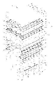
28b of the
board 28. The two boards 24, 28 are spaced apart by the egg-crate board 26.
Details of a
stacked patch radiator assembly which may be the same as or similar to
radiator assembly
22 are described in U.S. Pat. No. 6,624,787 B2 entitled "Slot Coupled,
Polarized, Egg-
Crate Radiator" assigned to the assignee of the present invention
[0084] The dual stacked-patch, egg-crate radiator assembly 22 is disposed over
the
LIME board 36 which is provided from polarization and feed circuit boards 40,
38. The
polarization and feed circuit boards 40, 38 are provided from a plurality of
RF printed
circuit boards 100 ¨114. Circuit boards 100, 102 comprise antenna element feed
circuits,
circuit boards 104-110 comprise power divider circuits and circuit boards 112,
114
comprise the polarizing circuit. In this exemplary embodiment, the
polarization, feed and
power divider circuits are all implemented as printed circuits but any
technique for
implementing low cost, low profile, functionally equivalent circuits may also
be used.
[0085] In this embodiment, circuit board 100 has a conductor disposed on a
surface
thereof. A pair of openings or slots 10 I a, 10Ib are 'formed or otherwise
provided in the
conductor 101 and RF signals are coupled to antenna elements 15a, 15b through
the slots
1 0 la, 101 b. The tile sub-array thus utilizes a balanced feed circuit (not
visible in FIG.
19
CA 02663800 2009-03-18
WO 2008/036469
PCT/US2007/074795
IC) which utilizes non-resonant slot coupling. The use of non-resonant slot
coupling
provides two benefits: first. use of slots (e.g. slots 101 a, 101b) helps
isolate the feed
network from the antenna element (e.g. antenna elements I5a, 15b) which can
substantially help prevent spurious radiation; and second, a non-resonant slot
can
substantially help eliminate strong back-lobe radiation (characteristic of a
resonant slot)
which can substantially reduce the gain of the radiator. In one embodiment in
which the
feed circuits are implemented as stripline feed circuits, the feed circuits
and slots are
isolated by plated through-holes (which act as mode suppression posts)
provided in
appropriate portions of the UML board 36.
[0086] UML board 36 (comprised of the polarization and feed circuit
boards 40, 38) is
disposed over the fuzz button board 50. Fuzz button board 50 includes one or
more
electrical signal paths 116 (only one electrical signal path 116 being shown
in FIG. IC).
The electrical signal path 116 provides an electrical connection between
circuits included
as part of the UML board 36 (e.g. polarization and feed circuits) and circuits
included on
the circulator board 60.
[0087] The circulator board 60 is comprised of live circuit boards 119 ¨ 123 a
magnet
125 (which is provided as a samarium cobalt magnet in one embodiment) and a
ferrite
disk 124 (which is provided as a Garnett ferrite in one embodiment) and a pole
piece 127
(which, in one embodiment, is provided as magnetizable stainless steel but
which can be
provided from any magnetizable material). Printed circuits provided on the
circuit board
121 complete the circulator circuit and provide signal paths for RF signals
propagating
through the circulator. In one embodiment, the circulator may be implemented
as the
type described in U.S. Patent 6,611,180 entitled Embebbed Planar Circulator
and
assigned to the assignee of the present invention and incorporated herein by
reference in
its entirety. The circulator hoard 60 is disposed over the "Fuzz Button" egg
crate board
70.
[0088] It should be appreciated that in an array antenna having a brick
style
architecture, circulators such as the RF circulator shown in FIG. IC, are
typically
incorporated into substrates included with each T/R channel.
CA 02663800 2009-03-18
WO 2008/036469
PCT/US2007/074795
[0089] In the present embodiment of the invention described herein, however,
the
design of the tile sub-array 12b removes the circulator from the T/R module
and embeds
it into a separate circulator board 60. For example, in the embodiment shown
in FIG. IC,
the RF circulator components (e.g. the ferrite 124 the magnet 125 and the pole
piece 127)
can be "buried" or "embedded" in a layer of commercially available material
such as a
low loss and low dielectric constant polytetralluoroethane (PTFE) based
materials. Thus,
circuit boards 119¨ 123 may be provided as PTFE based circuit boards.
[0090] By providing the circulator as an embedded circulator (rather than
as part of the
I 0 T/R module), a significant reduction in T/R channel size is provided.
By reducing- the
size of the T/R channel, a tighter lattice spacing in the antenna elements of
the tile sub-
array can be achieved. Tight lattice spacing is desirable since it is
important in wideband
phased array applications for achieving grating-lobe free scan volumes.
Moreover, the
embedded circulator can be provided utilizing commercial batch processing-
techniques
and commercially available materials which results in a lower cost phased
array.
[0091] The Fuzz-Button, egg-crate board 70 is provided from an egg crate board
71.A
T/R module 76 is disposed in openings provided in the board 70. The T/R module
is
provided having a ball grid array (BGA) 126 provided thereon. The T/R module
76
includes a first signal port which is electrically coupled to ball 126a and a
second signal
port which is electrically coupled to ball I 26b. The BGA 126 is electrically
coupled (e.g.
via soldering or any other technique for making- electrical connections well
known to
those of ordinary skill in the art) to electrical circuits and signal paths
provided in the
LML board 80 over which the T/R module 76 is disposed. The board 71 also has a
fuzz
button signal path 116 provided therein through which RF signals may propagate
from
the second port of the T/R module 76 through ball I26b and an electrical
signal path on
the LML board 80 to the circulator board 60.
[0092] In this exemplary embodiment, the LML board 80 is comprised of two sets
of
printed circuit boards 130, 132 with each of the two sets 130, 132 themselves
being
comprised of a plurality of printed circuit boards 134 ¨ 144 and 146 ¨ 154. It
should be
noted, as will be understood by those of ordinary skill in the art, bonding
adhesive layer
are not shown as part of PCBs 130, 132 but are shown with PCBs 38 and 40 in
the
21
CA 02663800 2009-03-18
WO 2008/036469
PCT/US2007/074795
UMLB 36. In this embodiment, the circuit boards 130 (and hence circuit boards
134-144)
correspond to the RF portion of the LML board 80 while the circuit boards 132
(and
hence circuit boards 146-154) correspond to the DC and logic signal portion of
the LML
board 80 with board 154 being disposed on the thermal spreader plate 86.
10093] A plurality of thermal paths designated by reference number 162
facilitate the
transfer of heat from the T/R module 76 through the LML board 80 and to the
thermal
spreader plate 86 which in preferred embodiments is provided as a cooled
thermal plate.
In this embodiment, the heat spreader plate 86 is coupled to board 154 of the
LML board
80 via a thermally conductive epoxy. Once boards 130, 132 are assembled (e.g.
bonded
or otherwise coupled together) to form the LML board 80, thermal pins 162
(only two of
which are labeled in FIG. IC) are shaken into holes in the LML board 80 until
the barbed
first end of the pins 162 are seated in the holes to ensure proper contact
with the BGA
126. The second end of the pins 162 extend a short distance through the LML
board 80
such that the second end of the pins 162 are disposed in holes 165 in the
thermal spreader
plate 86. The holes 165 are then tilled with a thermally conductive epoxy.
Thus, the
BGAs 126 provide a means to accomplish the coupling of RF signals, DC and
logic
signals and thermal transfer from the T/R modules 76.
[0094] It should also be appreciated that other techniques, may of course,
also be used
to couple the spreader plate 86 to the LMLA 20. Also, it should be appreciated
that
regardless of the precise location of the spreader plate on the tile 12b and
regardless of
how the spreader plate is coupled to the tile 12b (e.g. thermally conductive
epoxy, solder,
thermal grease, etc...), it is preferred that thermal paths (such as thermal
paths 162)
couple heat cwneratirw, devices such as T/R modules 76 to the heat sink such
as spreader
plate 86.
[0095] RF connector 91 b is coupled to an RF signal path 168 in the LM LA
20. In this
particular embodiment, the RF connector is provided as a GPPO connector but
any RF
connector having electrical and mechanical characteristics appropriately
suited for a
particular application may be used.
[0096] As indicated by the dashed line labeled with reference number 168, an
RE
22
CA 02663800 2009-03-18
WO 2008/036469 PCT/US2007/074795
signal fed into port 9 lb is coupled through the LML board 80 and is coupled
through the
BGA I 26a to the T/R module 76. The RF signal propagates though the T/R module
76
and is coupled through the BGA 126b along a signal path between boards 134,
136 and to
the signal path 116 in the fuzz button egg-crate board 70. The signal path 116
leads to
the circulator board 60, through signal path 116 in board 50 and through a
series of RF
signal paths provided from circuits on the UML board 36. RF circuitry on the
UML
hoard 36 splits the signal 168 into two portions 168a, 168b which are coupled
to the
radiator layer 22. It should be appreciated the circulator board 60 and the
T/R module 76
operate to make the system hi-directional. That is, port 91b may act as either
an input
I 0 port or an output port. In this manner, signals 168 are coupled to a
column of antenna
elements in the tile sub-array (e.g. column I 4a of tile sub-array 12b shown
in FIG. I B).
[0097] As those skilled in the art will appreciate, the layers of the
UMLA (and the
LMLA as well) can be fabricated from virtually any PTFE based material having
the
desired microwave properties. For example, the present embodiment, the printed
circuit
boards included in the UMLA and LMLA are fabricated with material reinforced
with
woven glass cloth.
[0098] It should be appreciated that the LM LA integrates the package-
less 117R channel
and the embedded circulator layer sub-assembly. As mentioned above, in
preferred
embodiments, the LMLA is bonded to the UMLA using the ball grid array (BGA)
interconnect approach. The package-less T/R channel eliminates expensive T/R
module
package components and associated assembly costs. One key building block ofthe
package-
Less LMLA is the Lower Multi-Layer Board (LM LB). The LMLB integrates RF, DC
and
logic signal distribution and an embedded circulator layer. All T/R channel MM
IC's and
components, RF. DC/Logic connectors and thermal spreader interface plate can
be
assembled onto the LMLA usimi, pick and place equipment. FIG. 7 below
illustrates a direct
MM IC chip-attach embodiment in which MM IC chips are directly attached to a
bottom layer
of the LM LB for those applications in which it is desirable to have a
relatively hi!411 peak
transmit power per T/R channel.
[0099] Referring now to FIG. 2, a portion of an exemplary tile sub-array
200 includes
an upper multi-layer assembly (UMLA) 202 coupled to a lower multi-layer
assembly
23
CA 02663800 2009-03-18
WO 2008/036469 PCT/US2007/074795
(LMLA) 204 through a first interface 205, a circulator 206 and a second
interface 207.
Interface 205 may, for example, be provided as a type similar to Fuzz-button,
interface 50
described above in conjunction with FIGs. 1A-1C, circulator 206 may be
provided as a
type similar to circulator board 60 described above in conjunction with FIGs.
IA-IC and
interface 207 he provided as a type similar to fuzz-button, egg-crate
interface 71
described above in conjunction with FIGs. 1A-1C.
[0100] The UMLA 202 illustrates the type of circuitry which may included in a
UMLA
such as the UMLA 18 described above in conjunction with FIGs. IA ¨ IC. The
UMLA
202 includes antenna elements 208 electrically coupled to a feed circuit 210.
In a
preferred embodiment, the feed circuit 210 is provided as a balanced feed
circuit. In this
particular embodiment, the feed circuit 210 is shown as having a pair of ports
coupled to
an input of a polarization control circuit 211. In this particular embodiment,
the
polarization control circuit is provided from a power divider circuit 212
coupled to a
quadrature hybrid circuit 216. Those of ordinary skill in the art will
appreciate, however.
that circuitry other than power divider circuits and hybrid circuits may be
used to
implement a polarization control circuit.
[0101] In the exemplary embodiment of FIG. 2, the divider circuit 212 is
provided =from
a pair of Wilkinson power dividers 214a, 214b. In other embodiments, power
dividers
other than Wilkinson-type power dividers may also be used. Power divider
circuit 212
has a pair of ports 212a, 212b coupled to respective ones of ports 216a, 216b
ofthe
quadrature hybrid circuit 216. A second pair of ports of 216c, 216d of the
hybrid circuit
216 lead to UMLA ports 202a, 202b.
[0102] As mentioned above, UMLA 202 is intended to illustrate some of the
circuitry
included in a UMLA such as UMLA 18 described above in conjunction with FIGs.
IA ¨
IC. It should thus be appreciated that to promote clarity in the figure and in
the
corresponding description, antenna elements 208 represents only those antenna
elements
which are coupled to the LMLA via the UMLA 202. Thus, element 208 in FIG. 2
may
represent all of the antenna elements in a tile sub-array (e.g. in an
embodiment in which
the tile sub-array only includes a single LMLA) or alternatively, element 208
in FIG. 2
may represent only a portion of the total number antenna elements in a tile
sub-array (e.g.
24
CA 02663800 2009-03-18
WO 2008/036469
PCT/US2007/074795
in an embodiment in which the tile sub-array includes multiple LMLAs).
[0103] Stated differently, antenna elements 208 represent the portion of
the antenna
elements in a full tile sub-array which are coupled to the LMLA via the UMLA
202. As
described above in conjunction with FIG. IC, a tile sub-array (e.g. tile sub-
array 12b in
FIGs. I-1C) may be provided from a single UMLA (e.g. UMLA 18 in FIGs. 1A-1C)
and
have multiple LMLAs coupled thereto. Alternatively, a tile sub-array (e.g.
tile sub-array
12b in FIGs. 1-1C) may be provided from a single UMLA (e.g. UMLA 18 in FIGs. I
A-
B) and a single LMLA coupled thereto where the single LMLA includes the number
of
T/R modules needed to process all signals provided thereto from the UMLA.
[0104] It should be appreciated that LMLA 204 shown in FIG. 2 includes only a
single
transmit/receive. (T/R) channel coupled to the antenna element 208 through the
feed
network 210. Thus, a single TR channel is coupled to a single antenna element.
In other
embodiments, however, a single TR channel may be coupled to a plurality of
antenna
elements. Also, although the LMLA is shown to include only a single T/R
channel, in
other embodiments, each LMLA may be provided having multiple T/R channels.
[0105] In practical systems a full tile sub-array will include a
plurality of T/R channels
and it should be appreciated that, in an effort to promote clarity in the
description and the
drawings, only a single channel is used in the exemplary embodiment of FIG. 2.
Thus,
illustration of the LMLA as including only a single T/R channel is not
intended to be and
should not be construed as limiting.
[0106] It should also be appreciated that FIG. 2 shows the elements of a
single T/R
channel which may be of the type included in one of the tile sub-arrays I 2a ¨
12x
described above in conjunction with FIGs. 1-1C. Those of ordinary skill in the
art will
appreciate, of course, that each of the tile sub-arrays 12a-12X (FIG. 1)
provided in
accordance with various embodiments of the invention can, (and in general
will), include
a plurality of such T/R channels.
[0107] UMLA Ports 202a, 202b are coupled through interface circuit 205,
circulator
circuit 206 and interface 207 to ports 204a, 204b of the LMLA 204. In
particular.
CA 02663800 2009-03-18
WO 2008/036469
PCT/US2007/074795
interface circuit 206 includes signal paths through which RE signals can
propagate from
the UMLA to the LMLA. At least portions of the signal paths may be provided
from so-
called fuzz-button circuits as described hereinabove in conjunction with FIGs.
IA-IC.
[0108] The LMLA 204 includes a .T/R module 230. The T/R module includes a
receive
signal path 23 I and a transmit signal path 250. Signals from UMLA ports 202a,
202b are
coupled to the receive signal path 231 at ports 204a, 204c. Signals having a
first
polarization are coupled from the UMLA 202 to port 204a and signals having a
second
difTerent polarization are coupled from the UMLA 202 through circulator board
206 to
port 204c.
[0109] The receive signal path includes a pair of single pole double
throw (SPDT)
switches 232, 234. The switches 232, 234 cooperate to couple a desired one of
the two
signals (each having different polarizations) from ports 204a, 204c to an
input port of an
amplifier 236 which in preferred embodiments is provided as a low noise
amplifier
(LNA) 236. With the switches 232, 234 positioned as shown in FIG. 2, signals
at port
204a are fed to the input port of the LNA 236. With the switch arms of
switches 232,
234 positioned as shown in dashed in FIG. 2, signals at port 204c are fed to
the input port
of the LNA.
[0110] Signals fed to the LNA 236 are appropriately amplified and coupled to a
SPDT
switch 238. The switch arm of the SPDT switch 238 can be placed in either a
receive
position or a transmit position. In a receive position (as shown in FIG. 2),
the SPDT
switch 238 provides a signal path from the output of the LNA 236 to an input
of a phase
shifter 240. Signals are coupled though the phase shifter to an amplitude
control circuit
242 (e.g. an attenuator 242) to and RE I/O circuit 246. The circuit 246
couples RE. DC,
and logic signals into an out of the T/R module 230.
[01 III The SPDT switch 238, the phase shifter 240 and the amplitude
control circuit
242 are all also part of the transmit signal path 250. When the TR module is
in a transmit
mode of operation, the switch arm of the SPDT switch 238 is placed in the
transmit
position (i.e. so as to provide a low loss signal path between the phase
shifter 240 and the
input to the amplifier 252). With the arm of the switch 238 so positioned,
signals from a
26
CA 02663800 2009-03-18
WO 2008/036469 PCT/US2007/074795
transmit signal source (not shown in FIG. 2) are coupled through the RF
portion of
distribution circuit 246 through the attenuator 242, the phase shifter 240,
the switch 238
to the amplifier which is preferably provided as a power amplifier 252.
[0112] The power amplifier provides an appropriately amplified signal (also
referred to
as a transmit signal) through interface 207 to port 206a of the circulator
206. A second
port 206b of the circulator 206 is coupled through interface 205 to UMLA port
202b and
a third port 206b of the circulator is coupled to the termination 254 through
the switch
232.
[0113] The transmit signal is then coupled through the polarization
control circuit 211
to the feed circuit 210 and -finally to the antenna elements 208 which emit an
RF transmit
signal.
[0114] It should be appreciated that the T/R module 76 contains
substantially all of the
active circuitry in the tile sub-array 12. As described above in conjunction
with FIGs.
IC, the T/R module 76 includes transmit and receive signal paths and each path
is
coupled to the beamformer in the LMLA 20.
[0115] In one embodiment, the LNA 236 may be provided as a compact Gallium
Arsenide (GaAs) Low Noise Amplifier and the power amplifier 252 may be
provided as a
compact GaAs Power Amplifier. Although not shown in FIG. 2, in some
embodiments,
the TR module may also include a Silicon Germanium (SiGe) control monolithic
microwave integrated circuit (MM IC) to control some or all of switches 232,
234, 238,
phase shifter 240 or amplitude control circuit 242.
[0116] Referring now to FIG. 3, a UMLA 260 is comprised of an egg-crate
radiator
assembly 262 (which may be the same as or similar to assembly 22 described
above in
conjunction with FIGs. I- IC) disposed over a UMLB 264. UMLB 264 is comprised
of
two subassemblies 310, 312. Each of the subassemblies 310, 312 are -fabricated
and then
coupled via layer 274 to provide the UMLB 264. In preferred embodiments, the
layer
274 corresponds to a bonding layer 274. In one particular embodiment, the
layer 274
corresponds to a bonding layer 274 provided as a Cyanate Ester resin B-stage
(e.g. the
27
CA 02663800 2009-03-18
WO 2008/036469
PCT/US2007/074795
type manufactured by W. L. Gore & Associates and sold under the trade name
Speedboard-C6). The egg-crate radiator and UMLB subassemblies 262, 264 are
then
bonded or otherwise secured together to provide the UMLA 260. The Egg-Crate
Radiator 262 and UMLA 264 may be secured together accomplished via a
conductive
epoxy bond film. Those of ordinary skill in the art will appreciate, of
course, that any
other bonding or fastening technique well known to those of ordinary skill in
art and
appropriate thr securing together microwave circuit subassemblies may also be
used. It
should be appreciated that in preferred embodiments, the UMLA 260 is provided
as a
bonded assembly. However, in accordance with the present invention, the final
bonded
UMLA assembly is the result of multiple lamination, bonding and assembly
processes.
[0117] The multi-step lamination, fabrication and assembly process for the
UMLA
results in several advantages: (a) each subassembly 262, 310, 312 may be
separately
tested and any subassembly 262, 310, 312 which does not meet or exceed desired
electrical and/or mechanical performance characteristics may be identified and
either
repaired or not used to form a UMLA; (b) each subassembly 310, 312 may be
separately
tested and any subassembly 310, 312 which does not meet or exceed desired
electrical
and mechanical performance characteristics may be identified and either
repaired or not
used to form a UMLB; (c) separate fabrication of sub-assemblies 262, 310, 312
allows
the fabrication process for each subassembly to be separately optimized for
maximum
yield of that subassembly; (d) since only known "good" subassemblies 310, 312
are used
to .fabricate UMLBs, this results in a high-yield UMLB fabrication process;
(e) since only
known "good" subassemblies 262, 310, 312 are used to fabricate UMLAs, this
results in
a high-yield UMLA fabrication process; and (f) separate fabrication of sub-
assemblies
262, 310, 312 which are then secured together via bonding layers results in a
wider
choice of bonding adhesives and bonding temperatures for each subassembly 262,
310,
312 which leads to improved mechanical performance for each subassembly 262.
310,
312. Thus, the .fabrication and assembly approach developed for the UMLA 260
produces a robust mechanical design that significantly improves manufacturing
yield.
[0118] In one particular embodiment, the egg-crate radiator 262 and UMLB 264
sub-
assemblies are both 0.5m x 0.5m and thus the UMLA is .5 meters (m) long by .5
m wide
28
CA 02663800 2009-03-18
WO 2008/036469 PCT/US2007/074795
(1 9.7 in. x 19.7 in). The UMLA 260 is provided having a thickness or height
RI typically
of about .25 inches and comprises 1024 dual circular polarized RE channels
with each RE
channel weighing about 0.16 ounces (4.65 gr.). Furthermore, with the above-
described
multi-step lamination and fabrication process, each circuit layer of the UMLA
can be
fabricated using PWB industry standard processes and fabrication tolerances
and
commercially available materials.
[0119] In one embodiment, the two subassemblies 310, 312 are comprised of
laminated
layers of ten-mil thick Taconic RF-30 dielectric circuit boards 266, 268, 270,
272, 276,
278, 280, 282 separated by 2 mil thick layers of FEP bonding adhesive 267. As
mentioned above, the bond between the egg-crate radiator 262 and UMLB 264 can
be
accomplished via a conductive epoxy film. In a preferred approach, the
subassemblies
310, 312 are first secured together to form the UMLB 264 (i.e. boards 310, 312
are
bonded using Speedboard-C bonding adhesive between ground planes separating
the
subassemblies 310, 312) and the UMLB 264 is then secured to the egg-crate
radiator 262
to form the UMLA 260.
[0120] It should be appreciated that UMLB 264 includes a plurality of vertical
interconnects 290-306. The vertical interconnects 290-306 are also sometimes
referred to
herein as "RF vias." The RF vias 290-306 provide RE signal paths between
circuits or signal
paths provided on the different layers of the circuit boards 266 ¨ 282 which
comprise the
UMLB 264.
[0121] For example, in subassembly 310, circuit board 270 is provided having a
50 ohm
input port to 25 ohm output port Wilkinson resistive divider disposed on layer
270b thereof
(only a portion 320 of the resistive divider is visible in the cross-sectional
view of FIG. 3).
The portion 320 of the resistive divider is coupled through RF vias 294, 296
to a stripline
feed circuit 322 on layer 268a of circuit board 268 (only a portion only a
portion of the feed
circuit 322 being visible in the cross-sectional view of FIG. 3). The feed
circuit 322 then
provides RF signals to one or more slot radiators 314a. The slot radiators
excite a pair of
stacked patch radiators provided as part of the egg-crate radiator sub-
assembly 262.
29
CA 02663800 2009-03-18
WO 2008/036469 PCT/US2007/074795
[0122] Similarly, subassembly 312 includes a 50 ohm input port to 50 ohm
output port
three branch quadrature hybrid circuit 324 on layer 280b of circuit board 280
and a 50 ohm
input port to 25 ohm output port Wilkinson resistive divider 326 on layer 278a
of circuit
hoard 278 (only portions of the circuits 324, 326 being visible in FIG. 3).
The quadrature
hybrid 324 splits an input signal fed thereto and provides a +90 phase
relationship necessary
to provide polarization control in the antenna (e.g. in a polarization control
circuit such as
that described above in conjunction with FIG. 2). In particular, the +90
phase relationship
is necessary to achieve left hand and right hand circular polarization in the
antenna. The
Wilkinson resistive dividers 320 and 326 split the signal again to provide
spatially
orthogonal signals that feed the radiators 263a, 263b in the subassembly 262.
The resistors
improve axial ratio performance as the array is scanned off bore sight by
terminating odd-
mode excitation at the Wilkinson ports feeding 294, 296 and 304, 306. The
resistors can be
provided, for example, as part ofthe copper film such as Ome(,1,a-ply or
could be applied as
an ink or chip resistor directly to the copper circuit on the dielectric
material of the circuit
board. The RF interconnects 290, 302 electrically couple together the
quadrature hybrid
circuits 324 and the Wilkinson divider circuits 320 and 326 provided on layers
270b, 278a.
[0123] It should be appreciated that RF interconnects 294, 296
interconnect circuits
provided on layers within a single subassembly of the UMLB 264 (i.e.
subassembly 310).
Similarly, RF interconnects 292, 302 interconnect circuits provided on
different layers within
subassembly 312 (i.e. a single subassembly of the UMLB 264).
[0124] RF interconnects 290, 304 and 306, however, interconnect circuits
provided on
different layers within different subassemblies of the UMLB 264. For example,
the RF
interconnects 304, 306 electrically couple together Wilkinson divider circuits
326 provided
on layers 278a and feed circuits 322 provided on layer 268a while RF
interconnect 290,
electrically couples together quadrature hybrid circuits 324 provided on
layers 280b and
divider circuits 320 provided on layer 270b. Since RF interconnect 290, as
well as RF
interconnects 304, 306, extend from the bottom-most layer of the UMLB 264
(i.e. layer
282b) to the top-most layer of the UMLB 264 (i.e. layer 266a), the RF
interconnect 290, 304,
306 can couple circuits on any layer on the UM LB 264.
CA 02663800 2009-03-18
WO 2008/036469 PCT/US2007/074795
[0125] As mentioned above, for reasons including, but not limited to the cost
of
manufacturing the U M LA 260, it is desirable to use standard PWB
manufacturing- processes
to fabricate subassemblies 310, 312 of the UMLB 264.
[0126] When using such manufacturing techniques, however, an RF "stub" is
produced
from the standard drilling and plating process to produce an RF via (as well
as mode
suppression vias which can be provided surrounding the RE via as is generally
known). The
RE stub is that part of the RE via extending above and/ or below an
intersection (or_i unction)
between the RF via and a transmission line conductor (e.g. the center
conductor ofa stripline
RF transmission line). RE stubs are produced when two (or more) RF
transmission lines are
connected.
[0127] In the UM LA of HG. 3, there are four distinct RE stubs produced in the
U M LB
from drilling and plating an RE via to connect two inner circuit layers.
First, in subassembly
310, stubs 390, 392 occur in the connection between the upper Wilkinson
divider circuit
layer (e.g. circuit 320 on layer 270b) and the feed circuit layer (e.g.
circuit 322 on layer
268a). Second, in subassembly 312, stubs 393, 394 occur in the connection
between the
quadrature hybrid circuit layer (e.g. circuit 324 on layer 280b) to the lower
Wilkinson divider
circuit layer (e.g. circuit 326 on layer 278a). Third, the stubs 420 (FIG. 5)
and 422 occur in
the connection between the quadrature hybrid circuit layer (e.g. circuit 324
on layer 280b)
and the upper Wilkinson divider circuit layer (e.g. circuit 320 on layer
270b). Fourth,
although not shown in FIG. 3, stubs can occur as a result of connections
between the lower
Wilkinson circuit layer (i.e. layer 278a) and the feed circuit layer (i.e.
layer 268a). It should
he appreciated that the third and fourth situations occur when subassembly 310
is bonded or
otherwise secured to subassembly 312. Thus, the stubs can occur as a result of
the
connections between circuits on different layers within in a single
subassembly or as a result
of the connections between circuits on different layers in multiple
subassemblies.
[0128] In conventional microwave assemblies having multiple circuit
boards and circuit
layers, the RE stubs are removed by a separate so-called "back-drill
operation" in which the
stub portion of the RE via is physically removed by drilling the RE via using
a drill diameter
larger than the diameter of the RF via. The resulting hole remaining after the
drilling
operation is back-filled with a non-conductive epoxy.
31
CA 02663800 2009-03-18
WO 2008/036469 PCT/US2007/074795
[0129] his added manufacturing step (i.e. the back-drill operation) has
two consequences.
First, RE performance is degraded by the dielectric "stub" extending beyond
the RE junction.
The epoxy filling typically does not match the surrounding microwave laminate
electrical
properties of d ielectric constant and loss and mechanical properties such as
the coefficient of
thermal expansion in the x, y and z directions are not matched between the
epoxy and
microwave laminate. Thus, the operating bandwidth of the RE interconnect is
reduced and
channel to channel tracking of RF performance (return loss, insertion loss) is
degraded.
Second, the process adds significant cost and lead time. These two
consequences are a result
1() of at least manufacturing tolerances and variations between the
electrical and mechanical
characteristics of the fill material and the circuit boards and reduce the
system performance
capabilities.
[0130] The tile sub-array of the present invention, however, eliminates
back-drill and
I 5 back-fill of all RF via stubs by utilizing an "RE matching pad" whereby
the RF via stubs
are electrically "matched" over the RE operating frequency band. The RF
matching pad
technique is a technique in which conductive material is provided on the blank
lavers
(i.e., layers with no copper) or in ground plane layers (with relief areas)
enabling a
standard, low aspect ratio drill and plate manufacturing operation to produce
an RE via
20 that connects inner circuit layers and produces a low insertion loss RE
transition across
X-Band (8 GlAz ¨ 12 GI-1z). With the RF Matching Pad approach, all RF and mode
suppression vias can be are drilled and plated through the entire assembly at
the same
time. Manufacturing costs associated with back drill and back fill operations
are
completely eliminated. Moreover, RF performance has been improved because
channel
25 to channel variations due to drill tolerances and backfill material
tolerances have been
eliminated.
[0131] In the embodiment of FIG. 3, RE matching pads are provided from
conductive
disks (surrounded by an annular ring relief area) in ground plane circuit
layers (i.e. layers
30 266a, 268b, 270a, 272b, 274a, 278b, 280a, and 282b). The RF matching pad
technique is
a general approach which can be applied to any RE stub extending a quarter-
wavelength,
or less, beyond an RE junction formed by an intersection of an RF interconnect
and an
RF transmission line.
32
CA 02663800 2009-03-18
WO 2008/036469 PCT/US2007/074795
[0132] Referring 110W to FIGs. 4 ¨ 4C in which like elements of FIG. 3 are
provided
having like reference designations, RE interconnect 294 can be clearly seen to
extend
from a first end on laver 266a of circuit board 266 to a second end on layer
272b of
circuit board 272. As discussed above in conjunction with FIG. 3, RF
interconnect 294
couples transmission line 320 on circuit layer 270b to transmission line 322
on circuit
layer 268a. It should be appreciated that in the embodiment shown in FIGs. 3
and 4, the
RE transmission lines 320, 322 each correspond to center conductors of a
stripline
transmission line with conductors 320a, 320b and 322a, 322b, respectively,
I 0 corresponding to the ground planes of the stripline configuration.
[0133] A first RF stub 390 occurs as a result of the junction (or
intersection) between
transmission line 320 and RF interconnect 294 and a second RF stub 392 occurs
as a
result of the junction (or intersection) between transmission line 322 and RF
interconnect
294. The first end of RF interconnect 294 is provided having an RF matching
pad 407
provided from a first conductive region 408 coupled to RE interconnections
294. In this
exemplary embodiment, the first conductive region of the RF matching pad is
provided as
a disk-shaped conductor 408. The first conductive region (e.g. disk-shaped
conductor
408) is surrounded by a non-conductive relief area 409 which electrically
isolates
conductor 408 from the ground plane 322a. In this exemplary embodiment, the
relief
area 409 is provided as an annular ring defined by an a first inner diameter
and a second
or outer diameter.
[0134] Similarly, the second end of RE interconnect 294 is provided
having an RE
matching pad 410 provided from a first conductive region 411 surrounded by a
non-
conductive relief area 412 which separates ground plane 320b from the
conductor 411.
[0135] The size and shape of the RF matching pads 407, 410 are selected to
"tune" (or
"match") any impedance and/or transmission characteristics of the respective
RF stubs
392, 390. It should he appreciated that RF matching pad 407 need not be the
same size or
shape as the RE matching pad 410. That is, the diameters of the disks 408, 411
need not
be the same. Also, the inner and outer diameters of the annular rings 409, 412
need not
he the same. Rather, each RE matching pad 407, 410 is provided having a shape
and
33
CA 02663800 2009-03-18
WO 2008/036469
PCT/US2007/074795
dimensions (i.e. a size) which most effectively provides RF interconnect 294
having
desired mechanical and electrical performance characteristics.
[0136] Also, as illustrated in conjunction with FIGs. 6 and 6A below, the
shape of the
first conductive region of the RF matching pad need not be a disk. Rather the
first
conductive region of the RF matching pad may be provided having any regular or
irregular geometric shape. Likewise, the relief regions (e.g. regions 409,
412) need not
he provided haying an annular shape. Rather the relief regions may be provided
having
any regular or irregular geometric shape as long as the relief regions
substantially
electrically isolate the first conductive region of the RF matching pad (e.2-.
regions 408,
411) from the ground planes on the layer on which the first conductive regions
occur.
For example, as shown in FIG. 4, ground plane 322a is on the same circuit
layer as
conductive region 408. Thus, relief region 409 (regardless of its size and/or
shape and/or
the size and/or shape of the conductive region 408) should electrically
isolate conductive
region 408 from the ground plane conductor 322a.
[0137] It should also be appreciated that RF matching pads may be
utilized with
impedance matching sections of transmission line as illustrated by
transmission line
section 321 in FIG. 4C. The effect of the impedance characteristics of the
matching
section 321 should be taken into account when designing (i.e. selecting the
shape and
dimensions) of the RF matching pad 410.
[0138] Referring now to FIG. 4D, a plot of insertion loss vs. frequency
for the RE
interconnect 294 is shown.
[0139] Referring now to FIGs. 5 ¨ 5C in which like elements of FIG. 3 are
provided
having like reference designations, RF interconnect 290 can be clearly seen to
extend
from a first end on layer 266a of circuit board 266 to a second end on layer
282b of
circuit board 282. As discussed above in conjunction with FIG. 3, RF
interconnect 290
couples transmission line 320 on circuit layer 270b to transmission line 324
on circuit
layer 280b. It should be noted that transmission line 320 is located in
subassembly 310
and transmission line 324 is located in subassembly 312. Thus RF interconnect
290
passes through both subassembly 310 and subassembly 312.
34
CA 02663800 2009-03-18
WO 2008/036469
PCT/US2007/074795
[0140] It should be appreciated that in the embodiment shown in FIGs. 3 and
4A. the
RF transmission lines 320, 324 each correspond to center conductors of a
stripline
transmission line with conductors 320a, 320b and 324a, 324b, respectively,
corresponding to the ground planes of the stripline configuration.
10141] RF stubs 420, 422 occur as a result of the junctions (or
intersections) between
the transmission line 320 and the RF interconnect 290. An additional RF stub
422 occurs
as a result of the junction (or intersection) between the transmission line
324 and the RF
interconnect 290.
10142] To reduce the effect on the RF interconnect 290 due to the stubs 420-
422, the
RF interconnect 290 is provided having a plurality of RF matching pads 424,
426, 428,
430, 432. The RF matching pad 424 is provided from a first conductive region
434
coupled to the RF interconnect 290. In this exemplary embodiment, the first
conductive
region of the RF matching pad is provided as a disk-shaped conductor 434. The
first
conductive region 434 is surrounded by a non-conductive relief area 436 which
electrically isolates conductor 434 from the ground plane 322a. In this
exemplary
embodiment, the relief area 436 is provided as an annular ring defined by a
first (or inner)
diameter and a second (or outer) diameter.
?0
[0143] Similarly. RF matching pads 426, 428, 430, 432 each include respective
ones of
first conductive region 438, 440, 442, 444 surrounded by respective ones of
non-
conductive relief areas 439, 441, 443, 445. The relief areas 439, 441, 443,
445 each
electrically isolate the conductive regions 438, 440, 442, 444 from the ground
planes
320a, 320b, 450, 324b, respectively.
[0144] The size and shape of the RF matching pads 424 - 432 are selected to
"tune" (or
"match") any impedance and/or transmission characteristics of the respective
RF stubs
420, 421, 422. It should be appreciated that RF matching pads need not be the
same size
or shape as each other. That is, the diameters of the disks 434, 438, 440,
442, 444 need
not be the same. Also, the inner and outer diameters of the annular rings 436,
439, 441,
443, 445 need not be the same. Rather, each RF matching pad 424 - 432 is
provided
having a shape and dimensions (i.e. a size) which most effectively provides RF
CA 02663800 2009-03-18
WO 2008/036469 PCT/US2007/074795
interconnect 290 having desired mechanical and electrical performance
characteristics.
[0145] Also, as illustrated in conjunction with FIGs. 6 and 6A below, the
shape of the
first conductive region of the RF matching pads 424 ¨432 need not be a disk.
Rather the
first conductive region of the RF matching pad may be provided having any
regular or
irregular geometric shape. Likewise, the relief regions need not be provided
having an
annular shape. Rather the relief regions may be provided having any regular or
irregular
geometric shape as long as the relief regions substantially electrically
isolate the first
conductive region of the RF matching pad from the ground planes on the layer
on which
I 0 the first conductive regions occur. For example, as shown in FIG. 5,
ground plane 320a
is on the same layer as conductive region 438. Thus, relief region 439
(regardless of its
size and/or shape and/or the size and/or shape of the conductive region 426)
should
electrically isolate conductive region 438 from the ground plane conductor
320a.
[0146] It should also be appreciated that RF matching pads may be utilized
with
impedance matching sections of transmission line as illustrated by
transmission line
section 321 in FIG. 5C. The effect of the impedance characteristics of the
matching
section 321' should be taken into account when designing (i.e. selecting the
shape and
dimensions) of the RF matching pads.
[0147] Referring now to FIG. 5D, a plot of insertion loss vs. frequency
for the RF
interconnect 290 is shown.
[0148] Referring now to FIGs. 6 and 6A, a pair of geometric shapes 460, 462
are
illustrative of the shapes in which the first conductive region and/or the
relief areas of the RF
matching pads may he provided. As mentioned above, the first conductive region
of the RF
matching pad (e.g. regions 408, 411 in FIGs. 4A, 4B or regions 434, 438, 440,
442, 444 in
FIG. 5) may he provided having any regular or irregular geometric shape.
Likewise, the
relief regions (e.g. regions 409, 412 in FIGs. 4A, 4B or regions 436, 439,
441, 443, 445 in
FIG. 5) need not be provided having an annular shape. Rather, the relief
regions may be
provided having any regular or irregular geometric shape as long as the relief
regions
substantially electrically isolate the first conductive region of the RF
matching pad from the
ground planes on the layer on which the first conductive regions occur. Thus,
regardless of
36
CA 02663800 2009-03-18
WO 2008/036469 PCT/US2007/074795
their size and/or shape, the relief regions should electrically isolate the
conductive regions
from the ground plane conductor.
[0149] The conductive regions and relief regions of the RF matching pads may
he
provided having any shape including but not limited to rectangular, square,
circular,
triangular, rhomboid and arc shapes. Also, the conductive regions and relief
regions of the
RF matching pads may be provided from combinations of any of the above shapes.
Also, the
conductive regions and relief regions of the RF matching pads may be provided
from
combinations of any of regular and irregular shape.
10150] Referring now to FIG. 7, a tile subarray 470 includes a T/R module
circuit board
472 having disposed thereover an RF circuit board 474. Disposed over the RF
circuit board
is a DC/Logic circuit board 476. Disposed over the DC/Louie circuit board is a
circulator
circuit board 478. Each ofthe T/R module circuit board. RF circuit board.
DC/Louie circuit
board and a circulator circuit perform substantially the same functions as the
T/R module
circuits RF circuits, DC/Logic circuits and circulator circuits described
above in conjunction
with 1-71Gs. 1 A ¨ 2.
[0151] Lastly, disposed over the circulator circuit board is a UMLA 480. The
UMLA may
be the same as or similar to the UMLAs described above in conjunction with
FIGs. IA ¨ 5.
[0152] The exemplary embodiment of FIG. 7 illustrates that the T/R modules 472
may be
directly attached to a bottom layer of an LMLB. That is, direct MMIC chip-
attach approach
M IC chips not shown) to a bottom layer of the LM LB may be used. This
approach may
be advantageous in those applications in which relatively high peak transmit
power per T/R
channel is desired.
[0153] All publications and references cited herein are expressly
incorporated herein by
reference in their entirety.
[0154] In the Figures of this application, in some instances, a plurality
of elements may be
shown as illustrative of a particular element, and a single element may be
shown as
illustrative of a plurality of a particular elements. Showing a plurality of a
particular element
37
CA 02663800 2009-03-18
WO 2008/036469
PCT/US2007/074795
IS not intended to imply that a system or method implemented in accordance
with the
invention must comprise more than one of that element or step, nor is it
intended by
illustrating a single element that the invention is limited to embodiments
having only a sini,le
one of that respective element. Those skilled in the art will recognize that
the numbers of a
particular element shown in a drawing can, in at least some instances, be
selected to
accommodate the particular user needs.
[0155] The particular combinations of elements and features in the above-
detailed
embodiments are exemplary only; the interchanging and substitution of these
teachings
I 0 with other teachings in this and the incorporated-by-reference patents
and applications
are also expressly contemplated. As those skilled in the art will recognize,
variations,
modifications, and other implementations of what is described herein can occur
to those
of ordinary skill in the art without departing from the spirit and the scope
of the invention
as claimed.
[0156] Further, in describing the invention and in illustrating-
embodiments of the
invention in the figures, specific terminology, numbers, dimensions,
materials, etc.. are
used for the sake of clarity. However the invention is not limited to the
specific terms,
numbers, dimensions, materials, etc. so selected, and each specific term,
number,
dimension, material, etc., at least includes all technical and functional
equivalents that
operate in a similar manner to accomplish a similar purpose. Use of a given
word,
phrase., number, dimension, material, language terminology, product brand,
etc. is
intended to include all grammatical, literal, scientific, technical, and
functional
equivalents. The terminology used herein is for the purpose of description and
not
limitation.
[0157] Having described the preferred embodiments of the invention, it
will now
become apparent to one of ordinary skill in the art that other embodiments
incorporating
their concepts may be used. Moreover, those of ordinary skill in the art will
appreciate
that the embodiments of the invention described herein can be modified to
accommodate
and/or comply with changes and improvements in the applicable technology and
standards referred to herein. For example, the technology can be implemented
in many
other, different, forms, and in many different environments, and the
technology disclosed
herein can be used in combination with other technologies. Variations,
modifications, and
18
CA 02663800 2014-07-08
, . .
WO 2008/036469
PCT/US2007/074795
other implementations of what is described herein can occur to those of
ordinary skill in
the art without departing from the spirit and the scope of the invention as
claimed. It is
felt therefore that these embodiments should not be limited to disclosed
embodiments but
rather should be limited only by the spirit and scope of the appended claims.
[0158] The particular combinations of elements and features in
the above-
detailed embodiments are exemplary only; the interchanging and substitution of
these
teachings with other teachings in this and the referenced patents/applications
are also
1 0 expressly contemplated. As those skilled in the art will recognize,
variations,
modifications, and other implementations of what is described herein can occur
to those
of ordinary skill in the art without departing from the scope of the invention
as claimed.
Accordingly, the foregoing description is by way of example only and is not
intended as
limiting. The invention's scope is defined in the following claims and the
equivalents
thereto.
[0159] What is Claimed is:
39