Note: Descriptions are shown in the official language in which they were submitted.
CA 02664416 2009-03-25
Apparatus and method for optical analysis of value documents
[0001] The present invention relates to an apparatus and method for optical
analysis of value documents.
[0002] Value documents are understood here to be card- or in particular sheet-
shaped objects that represent for example a monetary value or an authorization
and/or are not to be producible at will by unauthorized persons. They
therefore have
features that are not easy to produce, in particular to copy, whose presence
is an
indication of authenticity, i.e. production by an authorized body. Important
exam-
ples of such value documents are chip cards, coupons, vouchers, checks and in
par-
ticular bank notes.
[0003] Value documents are often analyzed optically for recognition of
their type
and/or their state and/or for a check of authenticity. It is fundamentally
possible to
use ambient light for the analysis, but such analyses show excessive errors
due to
fluctuations in the properties of the ambient light.
[0004] Analysis is therefore done using apparatuses that possess an
illumination
device for illuminating with optical radiation of given properties at least a
part of a
value document portion determined by a recording area of the apparatus, and a
de-
tection device for detecting optical radiation coming from the recording area,
in par-
ticular a value document illuminated by the illumination device.
[0005] Although it is possible to use light sources such as halogen lamps
for il-
lumination, they consume a lot of power compared with the radiated power
emitted
in a desired spectral range and therefore require adequate cooling. They
further have
the disadvantage of not having a very long life. Furthermore, such light
sources
have considerable space requirements.
[0006] The present invention is therefore based on the problem of providing an
apparatus for optical analysis of value documents that permits good
illumination of
CA 02664416 2009-03-25
- 2 -
a value document to be analyzed while having a compact structure, as well as
of
specifying a corresponding method.
[0007] This problem is solved by an apparatus for optical analysis of at
least one
value document in a recording area of the apparatus, having an illumination
device
for illuminating the value document in at least a part of the recording area
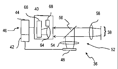
and pos-
sessing at least one surface emitting laser diode, and a control device for
driving the
laser diode, and a detection device for recording optical radiation from at
least a part
of the recording area.
[0008] The problem is further solved by a method for optical analysis of a
value
document in a recording area wherein the value document is illuminated with at
least one surface emitting laser diode.
[0009] In the method it is possible to preferably record optical radiation
from at
least a part of the recording area that occurs through the illumination of the
value
document. This can be in particular luminescence radiation excited in the
value
document, optical radiation reflected by the value document or transmitted
there-
through.
[0010] The detection device can accordingly be disposed relative to the
illumina-
tion device and the recording area in particular in such a way that its
radiation entry
is located on the same side of the value document where it is illuminated, or
on the
opposite side. This means that the detection device can be so disposed that
analysis
is possible with incident or transmitted light or in reflection or
transmission.
[0011] The analysis can fundamentally be done when the value document is at
rest relative to the analysis apparatus and in particular to the illumination
device.
However, in particular upon use in a value document processing apparatus in
which
value documents are analyzed automatically in succession, the value document
can
also be moving during illumination. The subject matter of the invention is
therefore
also an apparatus for processing value documents, hereinafter also referred to
as a
CA 02664416 2009-03-25
- 3 -
value document processing apparatus, having an inventive analysis apparatus
and a
transport device for moving a value document through the recording area at a
given
transport speed. The transport speed can be given in particular in dependence
on
properties of the analysis apparatus or of the transport device. Upon
sequential de-
tection it is thus possible to obtain an image of the value document portion
moving
through the recording area.
100121 The invention departs completely from the conventional manners of illu-
mination. Although it is possible to use conventional edge emitting laser
diodes in-
stead of halogen lamps for illumination, they radiate optical radiation with a
very
inhomogeneous and not simply symmetric intensity distribution. This can impair
the analysis of the value document.
[0013] According to the invention, a surface emitting laser diode is used
for il-
lumination. A surface emitting laser diode is understood in the context of the
pre-
sent invention more precisely to be a vertical surface emitting laser diode or
in par-
ticular a semiconductor device also referred to in English as a "vertical
cavity sur-
face emitting laser" (VCSEL), whose laser resonator is aligned with its output
direc-
tion, in which radiation is to be coupled out of the laser resonator, at least
approxi-
mately perpendicular to the surface of the device or chip. In particular, the
laser
resonator of such surface emitting laser diodes can have reflection devices,
for ex-
ample reflecting layers or reflecting layer systems, extending at least
approximately
parallel to the surface.
[0014] Surprisingly, the use of such surface emitting laser diodes offers
not one
but several advantages for use in an apparatus for analyzing value documents,
also
referred to hereinafter as an analysis apparatus.
[0015] Further, they can be produced with large exit windows compared with
edge emitting laser diodes, so that the radiated beam is not, or hardly,
influenced by
diffraction on the edges.
CA 02664416 2009-03-25
- 4 -
[0016] Furthermore, surface emitting laser diodes have a beam profile that is
ro-
tationally symmetric in good approximation, which substantially facilitates a
beam
shaping with simple optical elements compared to edge emitting laser diodes.
[0017] Further, in surface emitting laser diodes the emission wavelength range
is
determined more strongly by the laser resonator than in edge emitting laser
diodes.
This allows narrower emission wavelength ranges and leads to higher thermal
sta-
bility of the emission wavelength range.
100181 The full width at half maximum (FWHM) of the emission spectrum is
preferably less than 1 nm.
[0019] Also, the spatial coherence of the emitted radiation is lower than
in edge
emitting laser diodes, so that speckle patterns can be largely or completely
avoided
on a value document illuminated with the laser diode.
[0020] Due to the favorable beam shape of the surface emitting laser diodes,
they
can be advantageously combined with each other for illumination purposes, so
that
besides the laser diode at least one further surface emitting laser diode is
used for
illumination in the method. It is therefore preferred in the analysis
apparatus that the
illumination device possesses at least one further surface emitting laser
diode for
producing a given illumination pattern in the recording area, and the control
device
is configured to drive the further laser diode.
[0021] In this case it is particularly preferable that the laser diodes are
configured
in a component or chip. Such a configuration is readily possible only with
surface
emitting laser diodes and has the advantage that it is easy to produce a large
array of
laser diodes. A further advantage is that only one component needs to be
handled as
the radiation source upon assembly of the analysis apparatus, which
substantially
simplifies production.
[0022] Particularly preferably, more than 50 laser diodes are disposed on a
com-
ponent.
CA 02664416 2009-03-25
- 5 -
[0023] The drive of the laser diodes by means of the control device can be ef-
fected in different ways. In the simplest variant, all laser diodes of the
illumination
device are driven jointly, so that the illumination pattern obtained in the
recording
area is determined substantially by the number and arrangement of the laser
diodes.
[0024] According to another embodiment, the illumination device has at least
two groups of surface emitting laser diodes which comprise the above-mentioned
surface emitting laser diodes, and the laser diodes of one group are drivable
inde-
pendently of those of the other group. The control device is configured to
drive one
group of laser diodes separately from the drive of the other groups of laser
diodes.
In the method the value document can then be illuminated with at least two
groups
of surface emitting laser diodes which contain the laser diode, the laser
diodes of
one group being driven separately from those of the other group. Thus, drive
of the
groups permits in particular a temporal and spatial variation of the
illumination pat-
tern, which offers the advantage of greater variability of the illumination. A
separate
or independent drive or drivability is understood here to mean that the laser
diodes
permit such a drive. Further, the control device must be able to drive the
groups in-
dependently of each other, whereby the drive of the two groups of laser diodes
can
of course be coupled, for example through a programming of the control device.
[0025]
According to a further embodiment, in the analysis apparatus the laser di-
odes are drivable singly and the control device is configured to drive the
laser di-
odes singly. If further surface emitting laser diodes are used for
illuminating the
value document in the method, the laser diodes can then be driven singly. In
par-
ticular, the drive can be effected independently or separately in the above-
mentioned sense. The possibility of singly driving laser diodes on a chip is a
further
advantage of surface emitting laser diodes.
[0026] The arrangement of the laser diodes and their drive permit the illumina-
tion pattern to be largely determined in its form when only a simple
illumination
optic is used, i.e. in particular an illumination optic with optical
components, such
CA 02664416 2009-03-25
= - 6 -
as lenses, that are rotationally symmetric at least approximately around an
optical
axis, optionally folded by deflecting elements, in the area of the beam path.
The use
of only such an illumination optic simplifies and cheapens the production of
the
illumination device.
[0027] An illumination device having a plurality of surface emitting laser
diodes
preferably configured in a chip or component can be used advantageously for
pro-
ducing an areal illumination pattern due to the form of the beam profile of
the laser
diodes. For this purpose, the analysis apparatus is preferably configured to
illumi-
nate a given area with an illumination pattern whose location-dependent
intensity
variation over the area illuminated by the laser diodes is smaller than 20% of
the
maximum intensity of the illumination pattern. In the method the laser diodes
can
be driven in such a way that the laser diodes illuminate a given area of the
value
document with an illumination pattern whose location-dependent intensity
variation
over the area is smaller than 20% of the maximum intensity of the illumination
pat-
tern. Such an illumination is particularly homogeneous and thus facilitates a
reliable
detection of features. The given area preferably has an extent greater than
0.5 mm2.
[0028] This homogeneity can fundamentally be obtained by using suitable opti-
cal components or homogenization devices in the analysis apparatus. However,
the
surface emitting laser diodes are preferably disposed relative to each other
for illu-
minating a given area with an illumination pattern so that the illumination
pattern
produced therewith has a location-dependent intensity variation over the area
smaller than 20% of the maximum intensity of the illumination pattern. This
makes
it possible to avoid the use of special optical components and in particular
that of
homogenization devices, such as diffusing disks, diffractive optical elements
or
light guides, which reduce the intensity of the emitted optical radiation. The
analy-
sis apparatus therefore particularly preferably has no homogenization
elements,
such as diffusing disks, light guides or microlens arrays, for homogenization.
CA 02664416 2009-03-25
. - 7 -
[0029] The center distance between next adjacent surface emitting laser diodes
of
the illumination device is for this purpose preferably smaller than 150 !AM.
[0030] According to a first variant, the laser diodes can be disposed in the
form
of a matrix in the analysis apparatus. They can be disposed in particular on
the grid
points of a rectangular or square grid. This permits a particularly simple
production
of a laser diode array on a chip, in particular since in the case of a single
drivability
of the laser diodes the corresponding signal connections can be simply
designed.
Furthermore, a particularly simple drive can be effected with this
arrangement.
[0031] In a second variant of the analysis apparatus, the laser
diodes are disposed
on the points of a hexagonal point grid. This arrangement has the advantage
that a
particularly dense arrangement of the laser diodes is obtained in a simple
manner,
thereby permitting a particularly homogeneous illumination pattern.
[0032] As stated above, the illumination pattern can be determined in the re-
cording area or on the value document at least in its form substantially by
the ar-
rangement of the radiating laser diodes. In the analysis apparatus the control
device
is therefore preferably configured to drive only some of the laser diodes in
each
case to emit optical radiation to produce a given illumination pattern.
Accordingly,
in the method the laser diodes are preferably driven to emit optical radiation
so that
a given illumination pattern is produced. This embodiment has the advantage
that,
depending on the configuration, a change of the illumination pattern requires
only a
change of the control device. If the latter is programmable, as is preferred,
it is even
only necessary to change the program.
[0033] Higher flexibility is obtained when, in a preferred embodiment of the
analysis apparatus, the control device is configured to drive the laser diodes
in de-
pendence on a signal or data stored in the control device in such a way that
the same
illumination pattern is producible at different given locations in the
recording area
in dependence on the signal or data. In the method the laser diodes can then
be
driven in such a way in dependence on a signal or data that the same
illumination
CA 02664416 2009-03-25
- 8 -
pattern is producible at one of at least two different locations in dependence
on the
signal or data. The signal can be for example read in from an external data
entry
terminal via an interface or transmitted by a device of the value document
process-
ing apparatus containing the analysis apparatus. The drive of the laser diodes
can
consist in particular in only some of the laser diodes being switched on or
off.
[0034] Thus, in a preferred embodiment of the analysis apparatus, the control
de-
vice can in particular drive the surface emitting laser diodes in such a way
that an
extension of a detection area of the detection device in the transport
direction is
smaller than the extension of the illumination pattern in the transport
direction, and
the illumination pattern extends further with respect to the detection area
regarded
in the transport direction than contrary to the transport direction. The
detection area
is understood here to be that portion of the recording area from which the
detection
device can receive optical radiation for detection, in particular except for
scattered
radiation alone. A signal or data on the transport direction can be made
available to
the control device in the above-mentioned ways, which effects the drive of the
laser
diodes in dependence on the signal or data. This permits two things to be
obtained
at the same time. Firstly, the greater extension of the illumination pattern
in the
transport direction permits a greater amount of optical radiation, i.e. more
energy, to
be radiated onto a given area of the value document, for example a track with
fea-
ture substances, upon an analysis, in particular a luminescence analysis, so
that the
strength of the detection radiation can be increased. Secondly, the adjustment
of the
analysis apparatus, more precisely, of the position of the illumination
pattern rela-
tive to the detection area, can be adjusted automatically in dependence on the
trans-
port device upon installation in the value document processing apparatus by
corre-
sponding signals being transmitted to the control device for example from a
drive
system of the transport device or another device of the value document
processing
apparatus or being entered manually via an interface. The analysis apparatus
can
therefore be designed and used as a simply configurable module.
CA 02664416 2009-03-25
- 9 -
[0035] In the embodiment just described, the drive can in particular be
switchable between two or more illumination pattern positions.
[0036] Alternatively or in combination, in the analysis apparatus the
control de-
vice can be configured to drive the laser diodes in such a way that an
illumination
pattern changing in time during illumination is produced in the recording
area. In
the method it is then preferred that the laser diodes are driven in such a way
that an
illumination pattern changing in time during illumination is produced. The
temporal
change can be in particular given, for example by a corresponding
configuration
and/or programming of the control device.
[0037] The illumination pattern can be changed here in any desired way; in par-
ticular the form of the illumination pattern can be changed. However, it is
preferred
for many applications that the laser diodes are driven in such a way that a
given il-
lumination pattern is moved in a given direction at a given speed. In the
analysis
apparatus the control device is then configured to drive the laser diodes in
such a
way that a given illumination pattern is moved in a given direction at a given
speed.
The motion needs only to be effected for a given period of time, for example
until
the recording area has been swept once by the illumination pattern. Further,
it is
assumed that the laser diodes are disposed suitably for producing the
illumination
pattern. This embodiment has a number of advantages since it is usable for
different
purposes.
[0038] This embodiment makes it possible in particular to record a one- or
two-
dimensional image sequentially. In particular, in this case in the analysis
apparatus
the detection device only needs to be configured to detect optical radiation
from the
recording area integrally or only one-dimensionally in a direction
perpendicular to
the moving direction of the illumination pattern. Integral detection is
understood
here to be a detection that is non-locally resolving at a given moment.
Consecutive
illumination of different locations during motion of the illumination pattern
and cor-
CA 02664416 2009-03-25
- 10 -
responding sequential detection thus make it possible to produce an image by
as-
sembling the data or signals recorded at each single detection into the image.
[0039] To permit a complete illumination that is as simple as possible to
produce,
the analysis apparatus can be configured in particular to produce a
rectangular, in
particular linear, illumination pattern.
[0040] The analysis apparatus can be used in particular for recording one-
or
two-dimensional bar codes through motion of the illumination pattern.
[0041] The value document can fundamentally be at rest during recording. How-
ever, for faster analysis of a large number of value documents with only one
analy-
sis apparatus, it is preferred in the method that the value document is moved
in a
given transport direction and at a given transport speed during illumination.
[0042] The motion speed of the illumination pattern can fundamentally be
differ-
ent from the transport speed.
[0043] However, in the method the value document is preferably moved in a
transport direction at a transport speed, the direction being the transport
direction
and the speed being the transport speed. In a particularly preferred
embodiment of
the processing apparatus for processing value documents, the transport device
is
then configured to move a value document through the recording area at a given
transport speed, and the control device is configured to drive the laser diode
in such
a way that the illumination pattern is moved in the transport direction at the
trans-
port speed. This embodiment makes it possible in a particularly advantageous
man-
ner for an area of the analyzed value document, in particular an optical
security fea-
ture, to be followed during detection, so that analysis is possible even at
very high
transport speeds.
[0044] In general, but in particular also in connection with the last
described em-
bodiment, it is possible in the analysis apparatus that the control device is
config-
ured to produce an illumination pattern in a given part of the recording area
in de-
CA 02664416 2009-03-25
- 1 1 -
pendence on position signals from a position detection device. In the method
it is
accordingly preferred that the laser diodes are driven in such a way that an
illumina-
tion pattern is produced in a given part of the recording area in dependence
on posi-
tion signals from a position detection device. This embodiment has the
advantage
that a device for determining the position of a value document or the position
of a
feature to be analyzed optically can be used to produce the position signal
represent-
ing the position, in particular relative to the analysis apparatus, and that
precisely
this feature can be illuminated and analyzed in dependence on said position
signal.
This permits the amount of data arising upon an analysis of the total value
docu-
ment to be strongly reduced, so that an analysis can be effected faster and an
evaluation device for evaluating the detection results can be constructed more
sim-
ply. In particular in the case that the detection device is configured for
locally re-
solved recording of optical radiation in at least one given spectral range, a
consider-
able data reduction and an increase in data processing speed can be obtained
when
following the feature.
[0045] Alternatively to, or in combination with, the previously described
em-
bodiments, in the analysis apparatus the detection device can be configured
for lo-
cally resolved recording of optical radiation in at least one given spectral
range, and
the control device configured to drive the laser diodes in such a way that a
variation
of a sensitivity of the detection device to the optical radiation in the
spectral range is
at least partly compensated in dependence on the location. In the method it is
ac-
cordingly preferred that the laser diodes are driven in such a way that a
variation of
a sensitivity of a detection device for locally resolved recording of optical
radiation
in at least one given spectral range is at least partly compensated in
dependence on
the location. In this way a local adaptation of the illuminance to the
sensitivity of
the detection device can be effected, even after a relatively long time,
thereby per-
mitting an exact optical analysis lastingly.
CA 02664416 2009-03-25
- 12 -
[0046] Within the scope of the invention the laser diodes can be operated as
con-
tinuously luminous or pulsed radiation sources, for which the control device
is then
configured accordingly.
[0047] The invention will hereinafter be explained more closely by way of ex-
ample with reference to the drawings. These show:
Fig. 1 a schematic representation of a value document processing apparatus
according to a first preferred embodiment;
Fig. 2 a schematic representation of an analysis apparatus of the value
docu-
ment processing apparatus in Fig. 1,
Fig. 3 a schematic plan view of an edge emitting laser diode,
Fig. 4 a schematic representation of a beam profile of the edge emitting
laser
diode in Fig. 3 in the form of a contour diagram,
Fig. 5 a schematic lateral sectional view of a surface emitting laser
diode,
Fig. 6 a schematic representation of a beam profile of the surface emitting
laser
diode in Fig. 5 in the form of a contour diagram,
Fig. 7 a schematic plan view of a chip of the analysis apparatus in Fig. 2
with a
matrix arrangement of surface emitting laser diodes,
Fig. 8 a lateral view and a plan view for two possible illuminations by
drives of
the laser diodes in Fig. 7,
Fig. 9 a schematic representation of a value document processing apparatus
according to a second preferred embodiment
Fig. 10 a schematic representation of a temporal evolution of an
illumination of a
value document transported in the value document processing apparatus
CA 02664416 2009-03-25
- 13 -
in Fig. 9, wherein the illumination pattern is guided after the value
document, in a lateral view and a plan view,
Fig. 11 a schematic representation of a temporal evolution of an
illumination of a
value document at rest wherein the illumination pattern is guided over
the value document, in a lateral view and a plan view,
Fig. 12 a schematic representation of a part of a detection device of an
analysis
apparatus according to a further embodiment of the invention, and
Fig. 13 a schematic plan view of a chip of the analysis apparatus in Fig. 2
with
an arrangement of surface emitting laser diodes on grid points of a hex-
agonal point grid.
[0048] A value document processing apparatus 10 in Fig. 1 which comprises an
apparatus for optical analysis of value documents 12, in the example bank
notes, has
an input pocket 14 for the input of value documents 12 to be processed, a
singler 16
which can access value documents 12 in the input pocket 14, a transport device
18
with a gate 20, and, along a transport path 22 given by the transport device
18, an
apparatus 24 for analyzing value documents which is disposed before the gate
20,
and after the gate 20 a first output pocket 26 for value documents recognized
as au-
thentic and a second output pocket 28 for value documents recognized as non-
authentic. A central control and evaluation device 30 is connected at least to
the
analysis apparatus 24 and the gate 20 via signal connections and is used for
driving
the analysis apparatus 24, evaluating check signals from the analysis
apparatus 24
and for driving at least the gate 20 in dependence on the result of evaluation
of the
check signals.
[0049] The analysis apparatus 24 in connection with the control and
evaluation
device 30 is used for recording optical properties of the value documents 12
and
forming check signals representing said properties.
CA 02664416 2009-03-25
-14-
100501 While a value document 12 is transported past at a given transport
speed
in a transport direction T given by the transport path 22, the analysis
apparatus 24
records optical property values of the value document, whereby the
corresponding
check signals are formed.
[0051] From the check signals of the analysis apparatus 24 the central
control
and evaluation device 30 determines upon a check signal evaluation whether the
value document is recognized as authentic or not according to a given
authenticity
criterion for the check signals.
[0052] The central control and evaluation device 30 has for this purpose in
par-
ticular, besides corresponding interfaces for the sensors, a processor 32 and
a mem-
ory 34 connected to the processor 32 and storing at least one computer program
with program code upon the execution of which the processor 32 controls the
appa-
ratus or evaluates the check signals and drives the transport device 18 in
accordance
with the evaluation.
[0053] In particular, the central control and evaluation device 30, more
precisely
the processor 32 therein, can check an authenticity criterion which includes
for ex-
ample reference data for a value document to be considered authentic which are
given and stored in the memory 34. In dependence on the determined
authenticity or
non-authenticity, the central control and evaluation device 30, in particular
the
processor 32 therein, drives the transport device 18, more precisely the gate
20, in
such a way that the value document 12 is transported, according to its
determined
authenticity, for storage into the first output pocket 26 for value documents
recog-
nized as authentic or into the second storage pocket 28 for value documents
recog-
nized as non-authentic.
[0054] The analysis apparatus 24 is shown more exactly in Fig. 2. It
comprises
an illumination device 36 for illuminating at least a part of a flat recording
area 38
in the transport path 22 which is reached via the transport path 22 by value
docu-
ments 12 to be analyzed, and a detection device 40. A control device 42 for
driving
CA 02664416 2009-03-25
.. - 15 -
the illumination device 36, and an evaluation device 44 for evaluating signals
from
the detection device 40 are combined in a programmed data processing device 46
which in this example comprises a processor (not shown) and a memory (not
shown) which stores a program, executable by the processor, for controlling
the il-
lumination device 36 and for evaluating the signals from the detection device
40.
The control and evaluation devices 42, 44 are connected to the central control
and
evaluation device 30 via a signal connection.
[0055] The illumination device 36 has a semiconductor device or a semiconduc-
tor chip 48 in which a matrix arrangement of at least fifty surface emitting
laser di-
odes 50 for emitting optical radiation in a given spectral range is configured
(cf.
Fig. 7), and an illumination optic 52. The latter possesses, along an
illuminating
beam path, a beam-concentrating optic 54, a deflecting element 56 for
deflecting the
optical radiation leaving the beam-concentrating optic into the recording area
38,
and a focusing optic 58 for focusing the deflected illumination radiation as
an illu-
mination pattern 60 onto an illumination field 62 in the recording area 38.
[0056] The spectral range is given by the type of value documents to be ana-
lyzed, more precisely of security features formed thereon. In this example,
lumines-
cence properties of the value documents are to be analyzed. For this purpose
the
spectral range is selected so that the excitation radiation for luminescence
of an au-
thentic value document is within the spectral range. The deflecting element 56
is
deflective for the excitation radiation, but in good approximation transparent
to the
luminescence radiation, so that the latter can pass through the deflecting
element 56
without deflection.
[00571 Optical radiation emanating from the recording area 38 or from a value
document 12 therein, i.e. detection radiation, is imaged into infinity by the
focusing
optic 58 and passes through the deflecting element 56 without deflection into
the
detection device 40, which in the example comprises a detection optic 64, a
spec-
trographic device 66, for example an imaging optical grating, illuminated by
means
CA 02664416 2009-03-25
- 16
of the detection optic 64, and detection elements 68 for recording the
intensity of
spatially separated spectral components of the detection radiation which are
pro-
duced by the spectrographic device 66. For transmission of detection signals
repre-
senting the intensity of the impinging spectral components to the evaluation
device
44 the detection elements 68 are connected thereto via signal connections. The
de-
tection device 40 therefore records the detection radiation in locally
unresolved
fashion, so that an integral recording of the detection radiation is given.
[0058] As illustrated in Fig. 7, the surface emitting laser diodes 50 are
disposed
in the semiconductor device 48 of the illumination device 36 in parallel rows
and
columns perpendicular to the rows, whereby the distance between next adjacent
la-
ser diodes is 110 trn immediately before the particular laser diode.
[0059] To distinguish clearly from conventional edge emitting laser diodes,
Fig.
3 shows a schematic plan view of a semiconductor device 70 with an edge
emitting
laser diode. The semiconductor device 70 has configured therein, parallel to
the sur-
face of the semiconductor device 70 or of the wafer for producing the
semiconduc-
tor device, a resonator 72 which on its edges 74 and 74' along a low indexed
lattice
plane is partly reflective to the laser radiation to be produced and in which
the laser
active zone, i.e. a p-n junction, of the laser diode is located. The output
laser radia-
tion is emitted, as indicated in Fig. 3, perpendicular to the edges 74 and 74'
and par-
allel to the surface. The beam profile, i.e. the intensity distribution over a
plane per-
pendicular to the beam direction, is shown in Fig. 4 schematically as a
contour dia-
gram in which x and y are Cartesian coordinates in the plane and the lines
represent
lines of equal intensity. One can clearly recognize a saddle shape of the
distribution,
which is therefore not rotationally symmetric.
[0060] Fig. 5 shows schematically, in contrast, a surface emitting laser
diode 76
wherein a substrate 78 has disposed thereon a resonator 80 which is given by
reflec-
tion structures or reflecting layer structures 84, 84', for example in the
form of inter-
ference layers, extending parallel to the substrate 78 and the wafer surface
82. The
CA 02664416 2009-03-25
- - 17 -
laser radiation is now emitted perpendicular to the surface 82 of the wafer or
the
substrate 78. For simplicity's sake the electrodes and the distribution of the
current-
carrying layers are not explicitly shown.
[0061] Fig. 6 shows, in a representation corresponding to Fig. 4, the
beam profile
of the laser beam emitted by the surface emitting laser diode. It is in good
approxi-
mation rotationally symmetric around the beam direction and is therefore very
well
suited for further beam shaping with a simple illumination optic with
spherical and
planar optical elements as in this embodiment.
[0062] The surface emitting laser diodes 50 are configured and contacted in
the
semiconductor device 48 so as to be singly drivable independently of each
other.
[0063] Number, arrangement and area of the surface emitting semiconductor di-
odes 50 and the illumination optic 52 are selected so that a contiguous areal
illumi-
nation field with a superficial extent of at least 0.5 mm2 can be illuminated
in the
recording area 38 homogeneously, i.e. with an intensity fluctuation based on
the
maximum intensity in the illumination area smaller than 20%.
[0064] The control device 42 is used for separately driving the laser
diodes 50. In
this embodiment the analysis apparatus 24 is designed as a module to be
installed in
a value document processing apparatus, said module being so constructed that
the
value documents 12 are fundamentally feedable thereto from opposite
directions.
[0065] To obtain as long an illumination as possible of luminescent
substances in
a value document to be analyzed, the control device 42 drives the laser diodes
50 in
such a way that an illumination field 62 or an illumination pattern 60
extending fur-
ther beyond a detection field 86 (cf. Fig. 8) contrary to the transport
direction T than
in the transport direction T is produced in the recording area 38. The
detection field
86 is defined in that, except for scattered radiation, only optical radiation
from the
detection field 86 can reach the detection device 40. This achieves that an
area on
the value document is exposed to the illumination or excitation radiation for
a time
CA 02664416 2009-03-25
.. - 18 -
that is longer than the time in which it is located in the detection field 86.
This per-
mits an increased luminescence radiation to be obtained, which facilitates the
detec-
tion of the luminescence.
[0066] The control device 42 is so adapted, here through corresponding pro-
gramming, that upon a signal from the central control and evaluation device 30
which represents the transport direction T with respect to the position of the
analy-
sis apparatus 24, it drives the laser diodes 50 in such a way that one of the
two illu-
mination patterns 60, 61 shown in Fig. 8 is produced by the laser beams 88 in
the
recording area 38 in dependence on the transport direction T or the signal
represent-
ing it. They are shifted relative to the chip 48 so that the above-described
effect oc-
curs. For this purpose, only some of the laser diodes 50 are switched on,
namely the
laser diodes on the left (a)) or right (b)) in Fig. 8, while the others remain
switched
off The figure does not show the illumination optic 52 or its influence on the
beam
path for simplicity's sake. "Switched on" is understood here to mean that they
are
operated either continuously or also in pulsed fashion.
[0067] A second embodiment in Fig. 9 differs from the first embodiment in that
there is now disposed along the transport path 22 upstream of an analysis
apparatus
24' an image sensor 90 which is used for recording images of fed value
documents
and transfers the images to a central control and evaluation device 30' via an
image
signal connection. All other components are unchanged, so that the same
reference
signs are used for them as in the first embodiment and the comments on the
first
embodiment also apply accordingly here.
[0068] The central control and evaluation device 30' differs from
the central con-
trol and evaluation device 30 in that it has an interface (not shown in Fig.
9) for re-
cording the image data of the image sensor 90 and is configured, in the
example
through a corresponding program module, to determine from the image data the
position of an area of the value document, for example of a certain feature
area, to
be analyzed more exactly with the optical analysis apparatus 24' and to output
it to
CA 02664416 2009-03-25
_. - 19 -
the analysis apparatus 24'. The image sensor 90 therefore constitutes, in
conjunction
with the central control and evaluation device 30', a position detection
device.
[0069] The analysis apparatus 24' differs from the analysis apparatus 24 of
the
first embodiment solely in that the control device is now changed compared to
the
control device 42. The control device is, more precisely, configured to drive
the la-
ser diodes 50 differently from the control device 42. As shown schematically
in Fig.
in a time sequence a), b), c) in a manner corresponding to Fig. 8, the control
de-
vice drives the laser diodes 50 in such a way that laser diodes 92 at the
front in the
transport direction are switched on and laser diodes 94 at the back in the
transport
direction are switched off progressing in the transport direction T in each
case in
time sequence. This is effected in such a way that the same illumination
pattern 60'
or illumination field 62' which is produced from laser beams 88 of the front
laser
diodes is carried along directed onto the selected area 98 in the transport
direction T
at the transport speed T. Thus, in effect only the selected area 98 is
illuminated
while it is transported through the detection field 86. This makes it possible
to ef-
fectively reduce the production of scattered radiation or interfering
radiation from
other areas of the value document 12.
[0070] In other embodiments the image sensor 90 can also be replaced by other
devices, compared to the last embodiment, that permit recognition of the
position of
certain features to be analyzed. For example, it is also possible, depending
on the
feature, to use a signal from an edge detector for recognizing an edge of the
value
document leading in the transport direction, for example a light barrier or an
ultra-
sonic sensor, in connection with the known transport speed and the known
position
of the feature on the value document to produce a suitable position signal.
[0071] A further embodiment differs from the first embodiment in that for
analy-
sis of a value document the value document is stopped completely and after it
is
stopped in the recording area a start signal is outputted to an analysis
apparatus 24",
for which purpose the central control and evaluation device 30 is modified
accord-
CA 02664416 2009-03-25
- 20
ingly. The analysis apparatus 24" differs from the analysis apparatus 24 of
the first
embodiment solely by the configuration or programming of the control and the
evaluation devices 42, 44. For all other components the same reference signs
are
therefore used as in the first embodiment and the comments thereon also apply
ac-
cordingly here.
[0072] The control device is configured to drive the laser diodes 50 in such a
way
that they produce an illumination pattern changing in time during
illumination.
More precisely, the laser diodes are driven in such a way that the same
illumination
pattern 60" is moved over the value document 12 at a speed that is constant in
the
example, as illustrated in Fig. 11 corresponding in representation to Fig. 10
in a
time sequence a), b), c). At the same time the reflected detection radiation
is re-
corded at constant time intervals, in case of pulsed drive of the laser diodes
in syn-
chronism with the pulses, by the detection device 40 and the evaluation device
44
and stored in the evaluation device 44 according to the time sequence and thus
the
location on the value document, or transferred directly to the central control
and
evaluation device. Thus, an image of the value document is obtained.
Optionally
after intermediate storage in the evaluation device, the corresponding image
data are
transmitted to the central control and evaluation device 30 and evaluated
further
there.
[0073] The illumination pattern 60" has a rectangular slot shape, as
illustrated in
Fig. 11. The illumination pattern 60" is preferably so narrow that it can
serve as a
"virtual" entrance slit for the detection device or the spectrographic device,
which
then need no longer have an entrance slit.
[0074] Such an analysis apparatus can also be used advantageously for
recogniz-
ing bar codes. In particular in this case the detection device need then only
have a
detection element but not a spectrographic device.
[0075] In another variant, it is possible to provide in the detection
device, instead
of only one detection element, a row of detection elements by means of which
areas
CA 02664416 2009-03-25
- 21 -
in the recording or detection area are recordable in locally resolved fashion
along a
row perpendicular to the moving direction of the illumination pattern. Such an
analysis apparatus can in particular also be used for recording two-
dimensional bar
codes.
[0076] In a further embodiment, the analysis apparatus differs from the
analysis
apparatus of the first embodiment by a different detection device 40"' as well
as a
different control and evaluation device.
[0077] The detection device 40" (cf. Fig. 12) has a field 100 with a two-
dimensional arrangement of detection elements 102 for locally resolved
detection of
optical radiation coming from the recording area 38 or the detection field 86,
as well
as an imaging optic 104 for focusing the infinite beam path after the focusing
optic
58 onto the arrangement of detection elements 102. The detection elements 102
can
have different sensitivities to optical radiation in the same spectral range,
for exam-
ple due to fluctuations during production or to different aging.
[0078] The control device 42" is changed, i.e. configured, as opposed to
the con-
trol device 42 in such a way as to drive the laser diodes 50 according to the
sensitiv-
ity of the detection elements 102 in such a way that the differences in
sensitivity are
evened out. More precisely, this means that the laser diodes 50 are driven in
such a
way that all detection elements 102 output the same detection signals.
[0079] Errors in the imaging optic can also be compensated in this way.
[0080] The evaluation device 44" is configured to record the detection
signals of
the detection elements 102.
[0081] In a particularly preferred embodiment, the control device is
configured to
record the detection signals from the detection elements for a given drive of
the la-
ser diodes by means of the evaluation device, and to automatically change the
drive
of the laser diodes in such a way that all detection elements emit the same
detection
signal.
CA 02664416 2009-03-25
- 22 -
[0082] This
corresponds in a sense to a calibration of the analysis apparatus. This
process can, depending on the embodiment, be carried out automatically at
given
intervals in the service life of the analysis apparatus or upon each switch-on
or
switch-off of the analysis apparatus, for which purpose the control device can
be
configured accordingly, for example though corresponding programming.
[0083] Yet a further embodiment differs from the first embodiment only in that
the surface emitting laser diodes 50 are configured in the semiconductor
device and
contacted so as to be drivable separately or independently of each other in at
least
two groups, in this embodiment row by row. The control device 42 is
accordingly
modified in such a way as to drive the groups, i.e. here the rows, singly
separately
from each other, whereby the same illumination pattern as in the first
embodiment
can be obtained.
[0084] Further embodiments differ from the previously described embodiments
only by the arrangement of the laser diodes 50 in the semiconductor device
48'. All
other parts are unchanged. The surface emitting laser diodes 50 are now
disposed in
the semiconductor device 48' (cf. Fig. 13) on the grid points of a hexagonal
point
grid at a distance of nearest neighbors smaller than 120 Rm, in the example
100 ptm,
thereby making it possible to obtain a further increase in the homogeneity of
the
illumination pattern.
[0085] In yet further embodiments, the illumination device does not have the
de-
flecting element 56, so that a straight illuminating beam path is obtained.
The detec-
tion device is configured and disposed for detecting optical radiation after
transmis-
sion through the value document. It has its own optic, corresponding in its
proper-
ties to the focusing optic, for imaging at least a portion of the value
document on
the side not illuminated by the illumination device.
[0086] In other embodiments, the illumination of the value document can also
be
effected at angles other than 90 , in which case the detection device might be
con-
figured and disposed accordingly.