Note: Descriptions are shown in the official language in which they were submitted.
CA 02664862 2009-03-27
WO 2008/042015 PCT/US2007/009851
CAPACITIVE INTERFACE CIRCUIT
FOR LOW POWER SENSOR SYSTEM
TECHNICAL FIELD
[0001] The invention relates to sensor interface circuits and, more
particularly,
capacitive interface circuitry for low power sensor systems.
BACKGROUND
[0002] In micromachined systems, such as micro-electromechanical systems
(MEMS) sensors, variable capacitors serve as the interface between a sensor,
e.g.,
an accelerometer, gyroscope, pressure sensor, humidity sensor, or other types
of
micromachined sensors, and the measurement circuitry. Such sensors have a wide
variety of applications including industrial, environmental, and/or
physiological
monitoring. Physiological monitoring has various biomedical applications
including monitoring of posture, activity, gait, intravenous pressure,
intracranial
pressure, heart sounds, and the like.
[0003] In an accelerometer, for example, capacitive plates may be formed by
fingers on a beam coupled to a proof mass and fixed fingers coupled to an
inertial
frame. The sets of fingers are interdigitated and act as capacitor plates that
are
electrically connected to form variable, differential capacitors. A proof mass
is
suspended over a substrate by a spring. As the proof mass is deflected in a
particular direction, the capacitance measured between a beam finger attached
to
the proof mass and one of the corresponding fixed fingers coupled to the
inertial
frame changes, indicating acceleration in a particular direction.
[0004] Changes in capacitance due to acceleration along an axis are translated
to
output voltages by a capacitive interface circuit, which functions as sensing
circuitry. For an accelerometer, the capacitive interface circuit processes
signals
from the variable capacitors to produce sensor signals that represent
measurement
of motion. The accelerometer may sense motion along one axis, two axes, or
three
axes.
[0005] The variable, differential capacitors in the sensor can be generally
approximated as parallel-plate capacitors in which the overlapping area of the
1
CA 02664862 2009-03-27
66742-1215
plates or the spacing between the plates is a function of the displacement of
the
beam fingers. The output voltage of a typical switched-capacitor capacitance
sensing circuit can be calculated using the following equation:
vo= C Vs
i
where v,, is the output voltage of the capacitance sensing circuit, Cl is a
feedback
capacitance associated with the sensing circuit, A C is the change in
capacitance of
the variable capacitors, and Vs is the supply voltage.
(00061 Because of the size restrictions on the sense element in micromachined
systems, the capacitance of the variable capacitors and the change in
capacitance is
very small, e.g., approximately hundreds of ferntofarads to 1-100 attofarads.
When
the feedback capacitance is approximately the same size as the sense
capacitance,
the output voltage range is approximately 10 p.V to 1 mV and includes sampling
noise (kT/C noise). In general, kT/C noise refers to thermal noise in the
presence
of a filtering capacitor. The kT/C noise is caused by the reset switch of the
switched capacitor circuit and is sampled onto the sensing node of the
circuit.
Consequently, the sensor signal at the output of an amplifier may include
amplifier
offset, flicker noise (1/f) noise, and-kTIC noise that undermine sensor
accuracy and
performance.
2
CA 02664862 2009-03-27
66742-1215
SUMMARY
According to one aspect of the present invention,
there is provided a circuit comprising: means for
amplifying a differential sensor signal to produce an output
signal; a sampling capacitor that stores the output signal;
and means for applying a correlated triple sampling process
to reduce one or more noise components in the output signal,
wherein the means for amplifying comprises a first input
coupled to a first capacitive sensor element, a second input
coupled to a second capacitive sensor element, and an output
coupled to the sampling capacitor, and the means for
applying a correlated triple sampling process comprises: a
first switch that couples an output of the sampling
capacitor to ground during a first clock phase and decouples
Llle ouLpuL of Llle 5dltIplillg udpduiLor' from ground during a
second clock phase, a second switch that couples the first
input of the means for amplifying to ground during the first
portion of the first clock phase and decouples the first
input of the means for amplifying from ground during a
second portion of the first clock phase, a third switch that
couples the second input of the means for amplifying to
ground during the first portion of the first clock phase and
decouples the second input of the amplifier from ground
during the second portion of the first clock phase, and a
fourth switch that couples a reference voltage to the first
and second capacitive sensor elements during the second
clock phase and decouples the reference voltage from the
first and second capacitive sensor elements during the first
clock phase.
According to another aspect of the present
invention, there is provided a method comprising:
amplifying a differential sensor signal with a differential
amplifier to produce an output signal, the differential
2a
CA 02664862 2009-03-27
66742-1215
amplifier having a first input coupled to a first capacitive
sensor element and a second input coupled to a second
capacitive sensor element; storing the output signal on a
sampling capacitor that is coupled to an output of the
differential amplifier; and applying a correlated triple
sampling process to reduce one or more noise components in
the output signal, wherein the correlated triple sampling
process comprises: coupling an output of the sampling
capacitor to ground during a first clock phase and
decoupling the output of the sampling capacitor from ground
during a second clock phase, coupling the first input of the
differential amplifier to ground during a first portion of
the first clock phase and decoupling the first input of the
differential amplifier from ground during a second portion
of the first clock phase, coupling the second input of the
differential amplifier to ground during the first portion of
the first clock phase and decoupling the second input of the
amplifier from ground during the second portion of the first
clock phase, and coupling a reference voltage to the first
and second capacitive sensor elements during the second
clock phase and decoupling the reference voltage from the
first and second capacitive sensor elements during the first
clock phase.
2b
CA 02664862 2009-03-27
66742-1215
100071 This disclosure describes a capacitive interface circuit for a low
power
system. The capacitive interface circuit is configured to achieve very low
noise
sensing of capacitance-based transducers, such as a micro-electro-mechanical
system (MEMS)-based sensor, with high resolution and low power consumption.
The capacitive interface circuit uses a differential amplifier and correlated
triple
sampling (CTS) to substantially reduce kT/C noise and flicker (1/f) noise, and
suppress amplifier offset and drift. Rejection of kT/C noise may permit slower
interface clocks, and result in power reduction. The capacitive interface
circuit
may further include an output stage that reduces glitching in the output
signal by
allowing transients in the amplifier output to settle.
2c
CA 02664862 2009-03-27
WO 2008/042015 PCT/US2007/009851
[0008] In one embodiment, the invention provides a method comprising
amplifying a differential sensor signal to produce an output signal, storing
the
output signal on a sampling capacitor, and applying a correlated triple
sampling
process to reduces one or more noise components in the output signal.
[0009] In another embodiment, the invention provides a sensor device
comprising
a sensor, a differential amplifier that amplifies a sensor signal received
from the
sensor to produce an output signal, a sampling capacitor that stores the
output
signal, and a correlated triple sampling circuit that reduces one or more
noise
components in the output signal.
[0010] In an additional embodiment, the invention provides a capacitive
interface
circuit comprising a differential amplifier that amplifies a sensor signal to
produce
an output signal, a sampling capacitor that stores the output signal, and a
correlated
triple sampling circuit that reduces one or more noise components in the
output
signal.
BRIEF DESCRIPTION OF DRAWINGS
[0011] FIG. 1 is a block diagram illustrating a sensor device.
[0012] FIG 2 is a block diagram illustrating an interface circuit for use in
the
sensor device of FIG 1.
[0013] FIG 3 is a circuit diagram illustrating an example model for a sensor
in the
sensor device of FIG 1.
[0014] FIG. 4 is a circuit diagram illustrating one example of an interface
circuit
for use in the sensor device of FIG 1.
[0015] FIG 5 is a circuit diagram illustrating another example of an interface
circuit for use in the sensor device of FIG. 1.
[0016] FIG. 6 is a circuit diagram illustrating yet another example of an
interface
circuit for use in the sensor device of FIG. 1.
[0017] FIG. 7 is a circuit diagram illustrating a ping pong demodulator for
use with
any of the interface circuits of any of FIGS. 4-6.
[0018] FIG 8 illustrates timing waveforms for the interface circuits of any of
FIGS. 4-6.
3
CA 02664862 2009-03-27
WO 2008/042015 PCT/US2007/009851
[00191 FIG. 9 is a circuit diagram illustrating circuitry for an
instrumentation
amplifier for use in the interface circuit of any of FIGS. 4-6.
DETAILED DESCRIPTION
[00201 This disclosure describes a capacitive interface circuit for a low
power
sensor system. The capacitive interface circuit is configured to' achieve very
low
noise sensing via capacitance-based sensors, such as micro-electro-mechanical
system (MEMS)-based sensors, with high resolution and low power. The
capacitive interface circuit uses a differential amplifier and correlated
triple
sampling (CTS) to reduce kT/C noise and flicker (1/f) noise, and suppress
amplifier offset and drift. The capacitive interface circuit may further
include an
output stage that reduces glitching in the output signal by allowing
transients in the
amplifier output to settle. In this manner, the circuit can be used in a low
power
system to produce a stable, low-noise output.
[00211 The capacitive interface circuit may be configured to process signals
from a
sensing element in a MEMS-based sensor, such as an accelerometer, gyroscope,
pressure sensor, humidity sensor, or the like. Exemplary applications that may
use
a capacitive interface circuit in accordance with this disclosure include
physiological monitoring applications, such as monitoring of posture,
activity, gait,
intravenous pressure, intracranial pressure, heart sounds, humidity, liquid
level,
and the like. A capacitive interface circuit, as described herein, also may be
useful
in industrial or environmental monitoring applications, especially where very
low
power consumption is desirable.
[00221 In general, a capacitive interface circuit, as described in this
disclosure,
may be configured for very low power applications. Such low power applications
include a variety of medical and non-medical measurement applications. An
implantable medical device (IMD), for example, may be characterized by a
finite
power source that is required to last for several months or years. In some
cases,
the IMD may deliver a life sustaining therapy, such as cardiac pacing or
defibrillation, based on sensor input. Alternatively, the IMD may provide a
variety
of other beneficial therapies such as neurostimulation, e.g., for spinal cord
stimulation, pelvic floor stimulation, deep brain stimulation, gastric
stimulation, or
4
CA 02664862 2009-03-27
WO 2008/042015 PCT/US2007/009851
peripheral nerve stimulation. A sensor may be included in an IMD housing, lead
or catheter. A sensor associated with an IMD may be required to draw very low
power, yet provide precise and accurate measurement. Accordingly, it is
desirable
that sensing and therapy circuits associated with an IMD consume very small
levels of power to promote device longevity. As an example, operation of a
sensor
incorporating a capacitive interface circuit, as described in this disclosure,
may
require a supply current during continuous or periodic sensing in a range of
approximately 100 nanoamps to approximately 2.0 microamps, and more
preferably approximately 500 nanoamps to approximately 1.0 microamps. Sensors
operating within these ranges may generally be referred to as micropower
sensors.
.100231 According to various embodiments of this disclosure, a capacitive
interface
circuit may include a differential amplifier and a sampling capacitor coupled
to the
output of the differential amplifier. The capacitive interface circuit
operates uses
correlated triple sampling (CTS) signal processing techniques to substantially
eliminate kT/C noise, amplifier offset, and I/f (flicker) noise from the
output. As
the name suggests, CTS is a three-step process. The first two steps occur
during a
first clock phase and the third step occurs during a subsequent second clock
phase.
Generally, the CTS process substantially removes or eliminates the signal
components from the output of the amplifier that do not change between a first
clock phase and a subsequent second clock phase. The kT/C noise, amplifier
offset, and flicker (1/f) noise do not change between the first and second
clock
phase. Thus, these noise components are substantially eliminated from the
output
of the amplifier by the CTX process.
[0024] The first step is referred to as the reset step which resets the sensor
node
while the sampling capacitor is tied to a system ground. During the second
step,
referred to as the sampling step, kT/C noise from the variable sense
capacitors is
sampled onto the sampling capacitor through the differential amplifier. Offset
and
flicker noise are added to the kT/C noise by the differential amplifier and
collectively stored on the sampling capacitor.
[0025] The third step is referred to as the sensing step and involves applying
a
sensor signal to the differential amplifier. The differential amplifier
amplifies the
sensor signal to produce an output signal that includes an amplified
representation
CA 02664862 2009-03-27
WO 2008/042015 PCT/US2007/009851
of the sensor signal and a noise component. The sensor signal follows the same
signal path as the kT/C noise during the sampling step, the noise component of
the
differential output in the third step includes kT/C noise, amplifier offset,
and
flicker noise. Thus, the noise stored on the sampling capacitor substantially
eliminates the noise component of the output signal produced by the
differential
amplifier during the sensing (third) step.
[00261 The capacitive interface circuit may also include an output stage that
includes two interleaved sample-and-hold (S/H) stages. This output stage may
be
referred to as a ping-pong demodulator. In operation, one stage of the ping
pong
demodulator (ping stage) samples the output of the differential amplifier
during a
first clock cycle, while the other stage (pong stage) outputs a signal at the
same
time. The signal output by the pong stage is based on the output of the
differential
amplifier during the previous clock cycle. During a second clock cycle that
follows the first cycle, the ping stage outputs a signal based on the signal
sampled
during the first clock cycle and the pong stage samples the current output of
the
differential amplifier. In this manner, the two stages of the ping pong
demodulator
alternately sample the output of the differential amplifier and hold it for
one clock
cycle before outputting the signal. Holding the signal enables transients in
the
signal to settle so that the signal output by the ping pong demodulator
reduces
glitching and is more stable.
[00271 In addition, the capacitive interface circuit may provide negative
feedback
to. apply a counter charge that limits the signal. The negative feedback may
be
applied at the input to the output stage (ping pong demodulator) or applied as
global feedback to the input to the differential amplifier in order to keep
the signal
small. The feedback can be applied to both inputs of the differential
amplifier to
provide differential-to-single ended conversion. Furthermore, the capacitive
interface circuit may include additional signal processing circuitry, such as
an
analog-to-digital converter (ADC). In'such embodiments, the negative feedback
may be applied as discrete global feedback.
[00281 A capacitive interface circuit, in accordance with various embodiments
of
this disclosure, may produce a stable, low noise signal while operating with
very
low power. The circuit achieves low power by substantially eliminating noise
and,
6
CA 02664862 2009-03-27
WO 2008/042015 PCT/US2007/009851
more specifically, kT/C noise, from the output without requiring fast circuit
dynamics, i.e., operating at fast clock rates that draw more power. In fact,
the
circuit may operate with a clock rate of less than or approximately equal to
500 Hz
and, more preferably, approximately 200 Hz to approximately 300 Hz.
[00291 Various example embodiments are presented. According to some
embodiments, which is useful when the sensor interface nodes are isolated, the
interface circuit is configured so that a common plate can be driven and the
differential interface extracts the signal voltage which is proportionate to
the
difference in capacitance of the sense capacitors. This embodiment is useful
for
sensor architectures used for micromachined accelerometers.
[00301 According to other embodiments, which represents a modification of the
previous example embodiment, the interface circuit is configured to
accommodate
sensors that require one side of the differential plates of the sense
capacitors to be
held at common potential, e.g., a system ground. This latter example
embodiment
may be useful for pressure sensor architectures and may be extended to many
capacitive sensor applications, such as humidity sensors and liquid level
detection.
[00311 As mentioned previously, a capacitive interface circuit may be useful
in
conjunction with physiological sensors associated with IMDs. In these cases,
it is
important that the sensor provide low noise performance so that noise does not
result in reduced sensitivity or produce incorrect or misleading diagnostic
information. It is also important that the sensor operate with low power in
order to
conserve limited battery resources and thereby promote operational longevity,
particularly . A micropower sensor, as described in this disclosure, includes
a
sensor, such as a MEMS-based sensor, and a capacitive interface circuit
configured
to achieve stable, precise measurements with low power. Capacitive interface
circuitry and associated sensor circuitry may be useful in a wide variety of
applications. For purposes of illustration, however, use of such circuitry
will be
generally described in this disclosure in the context of medical applications.
[0032] FIG. 1 is a block diagram illustrating a micro-electromechanical system
(MEMS) sensor 2 that allows for measurement of capacitance fluctuations with
high resolution and low *power. As shown in FIG. 1, MEMS sensor 2 may include
a capacitor-based sensor 4 and a sensor interface 6 that interfaces with the
sensor.
7
CA 02664862 2009-03-27
WO 2008/042015 PCT/US2007/009851
MEMS sensor 2 may achieve accurate and stable measurement by substantially
reducing or eliminating kT/C sampling noise, as well as amplifier offset and
flicker
(1/f) noise, and reducing transients in the signal. Moreover, in some
embodiments,
MEMS sensor 2 may be configured to achieve this performance while operating at
a low clock rate, e.g., less than or equal to approximately 500 Hz,
approximately
200 Hz to 300 Hz, and more preferably approximately 250 Hz. As a result, in
some embodiments, MEMS sensor 2 can operate under the constraints of a micro
power system, e.g., draw approximately 100 nanoamps to approximately 2.0
microamps, and more preferably approximately 500 nanoamps to approximately
1.0 microamps of current from a power source.
[00331 For purposes of illustration, but without limitation, MEMS sensor 2 is
generally described in this disclosure as an accelerometer that enables
physiological inertial sensing in a chronically implanted device, i.e., an
implantable medical device (IMD). Physiological inertial sensing is important
because a patient's disease state or therapy disposition can be represented or
indicated by activity and posture. For example, delivery of some therapies may
be
controlled according to the activity, activity level, or posture of a patient,
or with
respect to detection of a disease state such as tremor or seizure in the cases
of
movement disorders or epilepsy. Accordingly, information provided by inertial
sensing is useful for diagnostic purposes and implementation of control loops
for
delivering therapy. For example, a chronic single axis MEMS sensor may be used
for adjusting cardiac pacing rate based on a patient's activity level. As
another
example, a multiple axis MEMS accelerometer may be used for adjusting therapy,
such as neurostimulation therapy, based on a patient's posture, i.e., sitting,
standing, lying down, or the like. When implanted within a patient, however,
MEMS sensor 2 should operate as a micropower system to conserve limited
battery resources thereby promoting operational longevity of the IMD. MEMS
sensor 2 should also maintain an acceptable noise floor, i.e., low noise
performance, so that noise does not cause reduced sensitivity or cause the
signal to
appear to show incorrect or misleading diagnostic information.
[00341 In order to operate within the power limitations of a micropower
system,
MEMS sensor 2 should be clocked at approximately 500 Hz or less. However,
8
CA 02664862 2009-03-27
WO 2008/042015 PCT/US2007/009851
because of the size restrictions on the sense element of a MEMS sensor, the
change
in capacitance of the variable capacitors is small, e.g., approximately
hundreds of
fFs to 100 aF or less. Thus, the output voltage range of a micropower MEMS
sensor may be approximately 10 V 'to approximately 1 mV when a feedback
capacitance associated with the sensor circuit is approximately the same size
as the
sense capacitance. At this small outpi4t voltage range, the signal at the
output of a
MEMS sensor includes kT/C noise as well as amplifier offset and flicker (1/f)
noise from the amplifier. The kT/C noise is caused by resetting the sensor
node
during the sampling process. These noise components can dominate the signal
voltage thereby undermining the accuracy and performance of the MEMS sensor.
[00351 MEMS sensor 2 utilizes a correlated triple sampling (CTS) process to
substantially eliminate kT/C noise, amplifier offset, and flicker (1/f) noise
from the
sensor signal. The CTS process does not require the clock rate to be increased
and,
thus, enables MEMS sensor 2 to operate under the power constraints of a
micropower system. MEMS sensor 2 also includes an output stage for reducing
transients in the signal chain to generate a stable output signal. The CTS
process
and output stage are described in greater detail below.
100361 In the example of FIG. 1, MEMS sensor 2 includes sensor 4 and sensor
interface 6 packaged on a substrate 8. Sensor 4 may be fabricated using MEMS
technology which uses micromachining processes to selectively etch away parts
of
the silicon substrate or add new structural layers to form mechanical and
electromechanical devices. MEMS technology integrates mechanical elements,
sensors, actuators, and electronics on a common silicon substrate. Sensor
interface
6 may be fabricated using integrated circuit processes and may be coupled to
sensor 4 via industry standard wirebonds.
(00371 Sensor 4 and sensor interface 6 may be separate discrete components on
substrate 8. Sensor 4 may, for example, be an off-the-shelf MEMS sensor, such
as
a micromachined single or multiple axis accelerometer. In this way, the
architecture of MEMS sensor 2 can partitioned to re-use existing sensor
technology
to leverage commercial volumes thus ensuring high reliability and low cost.
Reliability may be particularly important for sensor 4 if MEMS sensor 2 is
used for
9
CA 02664862 2009-03-27
WO 2008/042015 PCT/US2007/009851
monitoring of physiological signals, such as patient posture and activity, in
conjunction with an IMD.
[0038] Sensor interface 6 may be a specially designed component that provides
a
self-contained interface for reliable precision sensing at low power. In the
embodiment shown in FIG. 1, sensor' interface 6 is designed to transduce small
capacitive deflections from sensor 4 into a stable, precise analog output
signal with
low power. Sensor interface 6 may be manufactured separately from sensor 4,
but
calibrated and tested for operation with sensor 4. When sensor interface 4 is
received from the manufacturer, sensor 4 can be packaged on substrate 8 with
sensor interface 6.
[0039] In an exemplary embodiment, sensor 4 and sensor interface 6 may be
molded into land grid array (LGA) package on substrate 8. As an example, the
LGA package may have dimensions of approximately 3 millimeter (mm) in width,
by approximately 3 mm in length, by approximately 1 mm in thickness. The LGA
package protects sensitive high impedance nodes of MEMS sensor 2 from
environmental aggressors such as electrostatic discharge (ESD). MEMS sensor 2
may also be designed to be shock resistant to more than 10 kG. As a result,
MEMS sensor 2 may withstand abusive drops, such as dropping MEMS sensor 2
during a surgical implant procedure.
[0040] The LGA package may be hermetically sealed in a wafer-to-wafer bonding
step. A "cap" may be formed over substrate 8 to protect sensor 4 and sensor
interface 6 from moisture, plastic, and other contaminants in package
manufacturing. The cap also may serve as a substrate for die stacking sensor
interface 6 for small form factors in some embodiments. In an example
embodiment, sensor 4 may be held in a gas mixture that facilitates maintaining
a
finite sensor quality factor, Q, at resonance and provides nonlinear squeeze-
film
damping in the presence of shock. The sensor Q may be on the order of 8.
[0041] As described in FIG. 1, MEMS sensor 2 is generally implemented as part
of
an IMD. In one example, MEMS sensor 2 may be contained within the IMD
housing, sometimes referred to as a "can," or located on the device housing.
In
another example, MEMS sensor 2 may be located within a lead or catheter that
extends from the IMD, e.g., at the distal tip or at some point along the
length of
CA 02664862 2009-03-27
WO 2008/042015 PCT/US2007/009851
such a lead or catheter. In this case, MEMS sensor 2 may be electrically
coupled
to an IMD via electrical conductors in the lead that extend between MEMS
sensor
2 and the device can. This example embodiment may be useful when MEMS
sensor 2 is a pressure sensor used for monitoring heart sounds. The lead may
include conductors and electrodes for delivery of electrical stimulation
and/or
sensing. A catheter may include an inner lumen to deliver or withdraw fluids
from
a region within the body, and may include one or more conductor coupled to
sensor 2. Alternatively, sensor 2 may be equipped for wireless telemetry of
sensor
signals.
[0042] In general, sensor 4 converts mechanical energy into an analog output
voltage that is processed by sensor interface 6 to generate an output signal.
For
example, sensor 4 may be implemented as a micromachined three-axis
accelerometer that allows for inertial measurement with minimal area, power
penalty, and routing concerns by converting three axes of acceleration into
three
independent analog channels. Hence, sensor interface 6 may include multiple
interface circuits, each of which may be dedicated to one of the three axes.
The
three axes of acceleration may be aligned to the package dimensions, i.e., in
the x,
y, and z directions (length, width, and height). A suitable, exemplary process
for
fabrication of sensor 4 is the THELMA (Thick Epi-Poly Layer for Microactuators
and Accelerometers) process developed by ST Microelectronics, although other
MEMS processes may be used.
[0043] The architecture for the accelerometer may comprise, in some
embodiments, a single lateral accelerometer for measurement of x and y
acceleration, while measurement of acceleration along the z-axis may be
measured
using a differential teeter-totter arrangement. Other configurations are
possible for
sensor 4. Accordingly, the particular architecture described in this
disclosure is
exemplary as one of many possible configurations and should not be considered
limiting in any way. However, with respect to the example configuration
described in this disclosure, each axis of the accelerometer may use
differential
capacitors formed by interdigitated beam fingers to transduce acceleration
into an
analog output voltage. The interdigitated fingers act as capacitor plates that
are
electrically connected to form variable, differential capacitors. A proof mass
is
II
CA 02664862 2009-03-27
WO 2008/042015 PCT/US2007/009851
coupled to one set of the interdigitated fingers, referred to as the beam
fingers, and
suspended over the substrate by a spring. The capacitance between a beam
finger
attached to the proof mass and one of the corresponding fixed fingers changes
as
the proof mass deflects in a particular direction. The change in capacitance
indicates acceleration in a particular direction. Accordingly, sensor 4 may be
modeled by an equivalent set of capacitors in which the overlapping area of
the
plates or spacing between the plates is a function of the displacement of the
sense
element.
[00441 Sensor interface 6 is coupled to sensor 4 and translates the change in
capacitance to a voltage that is processed to produce sensor signals that
represent
measurement of motion. As previously described, the capacitance of the
variable
capacitors is typically within a range of approximately hundreds of fF and
exhibit
variation on the order of approximately 1 - 100 aF. As a result, the voltage
sensed
by sensor interface 6 may be within a range of approximately 10 V to 1 mV. If
MEMS sensor 2 operates as a micropower system, i.e., operates with a clock
rate
of approximately 500 Hz or less and draws less than approximately 2.0
microamps
of current form a power source, kT/C noise and other errors, such as amplifier
offset and flicker (1/f) noise, can dominate the signal voltage. Sensor
interface 6,
however, employs correlated triple sampling (CTS) to substantially eliminate
or
remove imperfections, i.e., kT/C noise, amplifier offset, and flicker noise,
from the
signal.
100451 As mentioned previously, CTS is a sampling process that eliminates
signal
components that do not change between the two clock phases of a clock cycle.
In
particular, CTS involves sampling a noise signal during the first clock phase
and
sampling a sensor signal during the second clock phase. Because the sensor
signal
follows the same signal path as the noise signal, the noise components, e.g.,
kT/C
noise, amplifier offset, and flicker noise, are common to both signals.
Consequently, kT/C noise, as well as amplifier offset and flicker noise, can
be
removed from the sensor signal by cancellation. In this manner, sensor
interface 6
produces a low noise sensor output signal.
[00461 Sensor interface 6 provides the interface for the CTS process. The
interface
includes a differential amplifier, a sampling capacitor, and a plurality of
switches.
12
CA 02664862 2009-03-27
WO 2008/042015 PCT/US2007/009851
Generally, the inputs of the differential amplifier are coupled to sensor 4
through a
pair of switches. The output of the differential amplifier is coupled to one
end of
the sampling capacitor. The other end of the sampling capacitor is coupled to
a
switch. In this manner, the switches are located at various nodes in the
signal path
and can be driven by respective clock signals to control the sequence of steps
of
the CTS process.
[0047] Again, the CTS process is a three step process. The first two steps
sample a
noise signal and occur during the first phase of a clock cycle. The third step
samples the sensor signal and occurs during the second phase of the clock
cycle.
The first step, also referred to as the reset step, resets the sensor node
during a first
portion of the first clock phase of the clock signal. The sampling capacitor
is also
tied to ground during the first step. In other words, the differential
amplifier in
sensor interface 6 is disconnected from sensor 4 during the first step to
build up
kT/C noise on the variable sense capacitors.
[0048] During the second step, which occurs during a second portion of the
first
clock phase, the differential amplifier is connected to the variable sense
capacitors
and the kT/C noise is sampled onto the sampling capacitor through the
differential
amplifier. The amplifier also introduces offset and flicker noise into the
signal,
which are collectively stored on the sampling capacitor with the kT/C noise.
[0049] The third step is initiated by the second phase of the clock cycle and
is
referred to as the sensing step. As the name of this step suggests, the sensor
signal
is applied across the variable capacitors to the differential amplifier. The
differential amplifier amplifies the amplitude of the voltage signal to
produce an
amplified signal. The amplified signal includes an amplified representation of
the
sensor signal and a noise component.
[0050] Because the sensor signal follows the same signal path as the kT/C
noise
during the sampling step, kT/C noise, amplifier offset, and flicker noise are
common between the two clock phases. That is, the noise component of the
amplified signal is substantially the same as the signal stored on the
sampling
capacitor during the sampling step. Thus, the noise signal stored on the
sampling
capacitor during the sampling (second) step substantially eliminates the noise
13
CA 02664862 2009-03-27
WO 2008/042015 PCT/US2007/009851
component of the amplified signal produced by the differential amplifier
during the
sensing (third) step.
[00511 The resulting signal, however, still may contain transients, i.e.,
glitches,
that are caused by fast dynamics in the signal chain. Accordingly, sensor
interface
6 may include an output stage coupled to the sampling capacitor that
suppresses
the clock transients. The output stage includes two interleaved sample-and-
hold
(S/H) stages and may be referred to as a ping-pong demodulator. One stage of
the
ping-pong demodulator (ping stage) samples the output of the differential
amplifier
during a first clock cycle and, more specifically, during the third step of
the CTS
process during the first clock cycle while the other stage (pong stage)
outputs a
signal at the same time. The signal output by the pong stage is based on a
signal
sampled from the differential amplifier during the third step of the CTS
process
from the previous clock cycle.
[00521 During a second clock'cycle that follows the first clock cycle, the
ping
stage outputs a signal based on the signal sampled during the first clock
cycle,
while the pong stage simultaneously samples the output of the differential
amplifier. In this way, the ping pong demodulator alternately samples the
output
of the differential amplifier and holds it for one clock cycle before
outputting the
signal at the following clock cycle. Holding the output for one clock cycle
allows
the transients (glitches) in the signal to settle. As a result, the output of
sensor
interface 6 in MEMS sensor 2 is a stable, low noise signal.
[00531 The output stage also may be configured to provide negative feedback
that
keeps signal change small. The feedback may be applied to the input of the
output
stage or, alternatively, may be applied globally to the input of the
differential
amplifier. When the feedback is applied as global feedback, the feedback is
differentially applied to the inputs of the differential amplifier to provide
differential-to-single ended conversion. The global feedback may be applied as
analog feedback or as discrete feedback. In the case of discrete feedback,
sensor
interface 6 may include an analog-to-digital converter (ADC).
[00541 In addition to the circuitry for the CTS process and output stage,
sensor
interface 6 may include supporting circuitry. For example, sensor interface 6
may
include a clock state machine, a reference and bias voltage generator, and on-
chip
14
CA 02664862 2009-03-27
WO 2008/042015 PCT/US2007/009851
trim memory for trimming offset and sensitivity. The on-chip memory may store
trim codes written in non-volatile memory during production to eliminate the
need
to track data through manufacturing. In particular, the trim codes may be used
by
sensor interface 6 to calibrate measurements obtained from sensor 4.
Furthermore,
interface circuit may provide an electro-static self-test that is used for
determining
the operability of MEMS sensor 2. The self test command may be useful in the
manufacturing process to determine if MEMS sensor 2 is operational before
shipping to a vendor. The self-test command may also be useful for validating
.
operation of MEMS sensor 2 when it is implanted within a patient and used for
monitoring physiological signals.
[00551 The output of sensor interface 6 may be passed to additional processing
circuitry off the chip, i.e., outside the LGA package. The additional
circuitry may,
for example, be a processor within an IMD or other device that processes the
output of MEMS sensor 2. For example, a processor within an IMD may process
the sensor output signal to identify characteristics in the signal that can be
used for
diagnostic purposes or to implement control loops for delivering therapy.
100561 Although MEMS sensor 2 is described in this disclosure as providing
sensing of physiologically-based motion, MEMS sensor 2 is not limited in this
way. Instead, it should be understood that MEMS sensor 2 and, more
particularly,
sensor interface 6, may be adapted to various medical and non-medical
applications. For example, sensor 4 may be any capacitive based sensor that
can
provide useful sensor data when used in conjunction with sensor interface 6.
Accordingly, sensor 4 may be a gyroscope, a pressure sensor, a microactuator,
or
other type of inertial, chemical, or magnetic sensor fabricated using MEMS
technology, including combinations of such sensors. MEMS sensor 2 may also be
used in catheter monitoring applications with pressure sensors, monitoring of
heart
sounds with pressure sensors, and other physiological monitoring applications
that
require micropower systems for precision measurements, such as acceleration,
pressure, humidity, and liquid level.
[00571 FIG. 2 is a block diagram illustrating various components of sensor
interface 6 of FIG. 1 in greater detail. As shown in FIG. 2, sensor interface
6
includes interface circuits 12X, 12Y, 12Z, trim memory register and circuit
10,
CA 02664862 2009-03-27
WO 2008/042015 PCT/US2007/009851
clock distribution network 18, and reference and bias generator 19. In the
example
of FIG 2, interface circuits 12X-12Z (collectively "interface circuits 12")
convert
three axes of acceleration (X, Y, and Z) into three independent analog output
channels (XOUT, YOUT, and ZouT). Hence, each of interface circuits 12
corresponds
to one of the X, Y and Z sensing axes. Each of interface circuits 12 may
include a
corresponding correlated triple sampler 14X-14Z (collectively "correlated
triple
samplers 14") and a corresponding ping pong demodulator 16X-16Z (collectively
"ping pong demodulators 16"), respectively.
[0058] Each of correlated triple samplers 14 produces a low noise signal at
its
output and includes a differential amplifier and a sampling capacitor coupled
to the
output of the differential amplifier. The differential amplifier may be an
instrumentation amplifier with a fully differential architecture that
interfaces with
sensor 4 to reject common mode signals and leakage current. The
instrumentation
amplifier may comprise a low-power instrumentation amplifier with stable gain
characteristics, good linearity, and wide common-mode range. An exemplary
instrumentation amplifier is illustrated in FIG. 9. Circuit diagrams of
exemplary
correlated triple samplers are illustrated in FIGS. 4, 5, and 6.
[0059] Each of ping-pong demodulators 16 receives the low noise signal
produced
by the corresponding one of correlated triple samplers 14 as an input and
outputs a
corresponding stable, low noise signal. Ping-pong demodulator 16 samples and
holds an output of the sampling capacitor 34 in first and second output stages
54A,
54B on an alternating basis. At the input of ping pong demodulators 16, the
low
noise signal may include transients that are caused by fast switching dynamics
in
the signal path. Ping pong demodulators 16 each include a pair of interleaved
output stages that alternately sample the output of the corresponding one of
correlated triple samplers 14 during a clock cycle and output the signal
during the
following clock cycle. In this way, ping pong demodulators 16 allow the
transients
in the signal to settle, e.g., for one clock cycle, before applying the
resulting stable,
low noise signal to additional processing circuitry. As previously described,
the
additional processing circuitry may include an ADC located on sensor interface
6
(not shown) or circuitry located off of sensor interface 6, such as circuitry
associated with the IMD that identifies characteristics in the signal that can
be used
16
CA 02664862 2009-03-27
WO 2008/042015 PCT/US2007/009851
for diagnostic purposes or implementing control loops for delivering therapy.
A
circuit diagram of an example ping pong demodulator is provided in FIG. 7.
[00601 Trim memory register and circuit 10 may include electrically erasable
programmable read only memory (EEPROM) cells or other cells of non-volatile
memory that store trim calibration codes. In-package memory, such as EEPROM
cells, allow for sensor device 2 to be calibrated on a high volume production
line
and then transferred for assembly as part of an IMD that delivers therapy to a
patient and uses output generated by sensor device 2 in a therapy delivery
algorithm, for diagnostic purposes, or both.
[00611 In some embodiments, trim memory register and circuit 10 may include an
offset trim block comprising a capacitor digital-to-analog converter (DAC)
that
injects charge onto the sensor nodes, thereby emulating a larger passive
coupling
capacitance between the clock and the amplifier. This capacitance is
independent
of the acceleration force.
[00621 An exemplary offset trim block may include reset switches required to
null
the sensor nodes during the reset phase of the sensor clock. The absolute
magnitude of the injected charge may be determined by integrated poly-poly
caps,
driven by the sensor clock. A binary weighted capacitor DAC code determines
the
relative magnitude of the injected charge and to which plate the charge is
routed.
The DAC code may be obtained from trim memory register 10.
[00631 Clock distribution network. 18 creates the signal chain and sensor
clocking
on-chip from a single master external clock. The master external clock may be
located off of sensor interface 6 and associated with processing circuitry for
the
IMD that uses the output of sensor interface 6. Clock distribution network 18
may,
for example, create one or more clock signals to control correlated triple
samplers
14 and ping pong demodulators 16. That is, clock distribution network 18 may
create clock signals that drive switches positioned at various nodes within
the
signal chain to control the sequence of steps of the CTS process.
[00641 For example, the nominal clock frequency for the signal chain may be
approximately 1 kHz, which is partitioned by clock distribution network 18
into
the phasing necessary to drive correlated triple samplers 14 and ping pong
demodulators 16. A clock driver for exciting sensor 4 may include a negative
17
CA 02664862 2009-03-27
WO 2008/042015 PCT/US2007/009851
charge pump that clocks sensor 4 to -AVDD on the sensor reset clock, and
+AVDD on the read-out portion. Significant capacitive loading on sensor 4 may
limit the negative clock to approximately' 80% of AVDD when using an on-chip
capacitor that can fit into the sensor package. This amount of drive is
sufficient for
meeting the noise requirements.
[00651 Reference and bias generator 19 provides reference and bias voltages
for
MEMS sensor 2. For example, generator 19 may supply reference voltages to
sampling capacitors in correlated triple samplers 14 and bias voltages to
active
circuit elements in interface circuits 12, such as the differential amplifiers
in
correlated triple samplers 14 and amplifiers in the S/H circuits in ping pong
demodulators 16.
[00661 The following description provides general part specifications of an
exemplary MEMS sensor. For example, an approximate maximum size of an
ASIC forming sensor interface 6 may be approximately 2,100 pm, by
approximately 1,300 m, hams and scribes not included. The sensor die may be
approximately 2,100 gm, by approximately 1,900 m. Sensor 4, protective cap,
and ASIC-based sensor interface 6 may be die stacked and placed in an industry
standard land grid array (LGA). In an'exemplary embodiment, the dimensions of
the LGA package may be approximately 3 mm in length, by approximately 3 mm
in width, by approximately 1 mm in height.
[00671 Reference and bias generator 19 may be supplied with a nominal supply
voltage for sensor interface 6 and a maximum supply voltage for programming
trim memory register 10. The nominal supply voltage and maximum supply
voltage may, for example, be 1.9 V (+/- 5%) and 14 V, respectively. The
minimal
supply voltage may be extended to 1.7V functionality, with some potential
derating
of the specifications for sensitivity and offset. The nominal supply current
for
MEMS sensor 2 may be a maximum of approximately 1 uA for continuous
measurement of three axis of acceleration. MEMS sensor 2 may also operate with
also be a low-power mode that lowers the current to approximately 500 nA.
These
values are merely exemplary and should not be considered limiting in any way.
100681 Additionally, there may also be a "sonogram mode" to measure cardiac
sonograms along the z-axis that draws a different amount of current than the
18
CA 02664862 2009-03-27
WO 2008/042015 PCT/US2007/009851
normal-mode, or low-power mode. The requirement driver for the sonogram mode
is 5 mg root-mean-square (rms) noise with a minimum 50 Hz bandwidth. The
nominal clock frequency for the signal chain is approximately 1 kHz, which is
partitioned by a small state machine into the phasing necessary to drive the
sensor
and the ping-pong demodulation amplifier. The clock driver for exciting the
sensor includes a negative charge pump, so that the sensor is clocked to -AVDD
on the sensor reset clock, and then +AVDD on the read-out portion. In
practice,
the significant capacitive loading on the sensor (e.g., approximately 6 pF)
limits
the negative clock to approximately 80% of AVDD when using an on-chip
capacitor that can fit into the sensor package. This amount of drive is
sufficient for
meeting the noise requirements.
[00691 The following briefly describes the nature and function of each of the
signals available at bonding pads (not shown) on sensor interface 6. Sensor
interface 6 may include six differential sensing pads, X+, X-, Y+,Y-, Z+, Z-,
a
common "rotor" drive COM, and two ground pads GND that are routed to all
sensors. The electrodes may be placed along the top of sensor interface 6. The
ordering of the electrodes may be GND : Z+ : Y+ : X+ : COM : X- : Y- : Z- :
GND. The pad pitch may be approximately 110 um. The COM pad centerline
may be coincident with the centerline of sensor interface 6, spaced
approximately
1050 urn from each edge.
[0070] To reduce input capacitance, there may be no electrostatic discharge
(ESD)
cells on these pads in some embodiments. ESD protection on the sensor pads may
be provided by series 500kW resistors sized for 2kV HBM (human body model).
The switch diffusions on the core protect the IC gates. The bond pads may be
bootstrapped by the sources of sensor interface 6 to lower capacitive load of
the
sensor.
[00711 A VSS and Vref pad provide a ground reference and a reference voltage,
respectively. Sensor interface 6 may also include pads for analog outputs,
e.g.,
XOUT, YOUT, and ZouT= The analog outputs XOUT, YOUT, ZOUT provide three
different channels for accelerometer signals along three different axes (X, Y
and
Z). The signal voltage may be centered about Vref/2 and the sensitivity may be
ratiometric to Vref. This allows for the use of a ratiometric ADC for robust
19
CA 02664862 2009-03-27
WO 2008/042015 PCT/US2007/009851
sensing. Vref may be tied to AVDD for ratiometric operation, or to a bandgap
for
an absolute reference. The output of sensor interface 6 may be able to source
a
minimum of approximately 50 nanoamps.
[0072] Sensor interface 6 may include an additional four pins through a serial
12C
port for programming the EEPROM cells of trim memory register and circuit 10,
providing the data, and for selecting whether trim codes come from volatile
registers or from the EEPROM in trim memory 10, respectively. Six bits of
offset
may be allocated to each axis for offset, and an on-chip digital-to-analog
converter
(DAC) (not shown) may deliver the offset charge to the sensor interface node.
The
offset for each axis may be trimmed to within 0.25G. Final calibration may be
performed after implant of an IMD based on final orientation of sensor 4 with
respect to earth. The sensitivity trim may adjust the scaling on output and
hold
capacitors in ping pong demodulators 16, and may set a net tolerance of
50mV/G/Vdd +/- 5%, where Vdd is the supply voltage
[0073] The target noise of the sensor channel may be approximately 500 g/rtHz
in
X and Y, and 750 .tg/rtHz in Z, for a sensor excitation voltage of
approximately
2.4V (2x bandgap). This will provide a nominal noise floor of approximately
2mg-
mis in X and Y and 3mg-rms in Z for posture detection (10Hz bandwidth, first
order lowpass). In some embodiments, the desired estimated noise floor
requirement may be 10mg-rms in a 10Hz bandwidth. The targeted lower noise
floor may capture the extreme process corners of a MEMS process without
compromising the power specification. MEMS sensor 2 may include a trim for
decreasing the quiescent current, if the MEMS process stability is found to
not
require the design margin.
[0074] In embodiments in which MEMS sensor 2 includes a pressure sensor for
measuring cardiac sounds, the Z-axis may also have a boost mode that decreases
the noise floor. In combination with a faster clock, the boost mode may
provide
approximately a 5mg-rms noise floor with a 100Hz effective noise bandwidth.
This mode may be used for monitoring cardiac sonograms in IMD applications.
[0075] The nominal bandwidth requirement for the X and Y accelerometer channel
may be approximately 20Hz (-3dB point). The minimum bandwidth for the Z
accelerometer channel may be approximately 50Hz (-3dB point) to allow for the
CA 02664862 2009-03-27
WO 2008/042015 PCT/US2007/009851
measurement of cardiac sounds. Additionally, the low-pass characteristic may
be
first-order and determined by capacitor ratios and the system clock in the
output
stages of interface circuits 12.
[0076] The cross-axis sensitivity of the accelerometer used for sensor 4
between
X, Y and Z axes may be under approximately 5%. The dominant error in cross-
axis sensitivity is package alignment. The non-linearity of MEMS-based sensor
device 2 may be less than approximately 5% for a specified range of +/- 6 G.
The
absolute offset of sensor 4 may be trimmed to +/- 0.5 G/s. When implemented as
an accelerometer within a patient to detect posture of the patient, the
orientation of
sensor 4 should be calibrated in the patient for posture. Thus, as long as the
dynamic range is acceptable, the absolute offset may not be critical. However,
the
offset of the accelerometer preferably should not drift more than +/- 100 mG
over a
temperature range of approximately 37 C +/- SC and over the lifetime of the
sensor. .
[0077] FIG. 3 is a circuit diagram illustrating sensor 4 of FIG. 1 modeled as
an
equivalent set of capacitors for purposes of illustration. The model of FIG. 3
represents a single axis of a multiple axis MEMS accelerometer. In FIG. 3,
sensor
4 includes sense capacitors 20A and 20B (collectively referred to as "sense
capacitors 20"), parasitic capacitors 21 A and 21 B (collectively referred to
as
"parasitic capacitors 21"), self test capacitors 22A and 22B (collectively
referred to
as "self-test capacitors 22"), and drive capacitor 24. Sense capacitors 20
represent
the variable capacitances of an accelerometer, which may be formed by
interdigitated fingers that act as capacitor plates.
[0078] A voltage is applied to sensor 4 through drive node 44, which is common
among the three sensor axes. Drive node-44 may be generated by sensor
interface
4. Thus, drive capacitor 24 represents the drive capacitance shared among the
three sensors for a multiple axis MEMS accelerometer. Each of sense capacitors
20 is coupled to drive node 44 on one side and shunted to ground on the other
side
through corresponding parasitic capacitors 21. Sense capacitors 20 are read
out
differentially by an interface circuit, such as one of interface circuits 12
in FIG. 2.
As an example, sense capacitances may be approximately 1 fF/G differential
with a
21
CA 02664862 2009-03-27
WO 2008/042015 PCT/US2007/009851
nominal sense capacitance of approximately 330 if. The capacitance of
parasitic
capacitors 21 may be approximately 1.4 pF.
[00791 In general, self-test capacitors 22 are coupled at one end to drive
node 44
and used to determine operability of sensor 4. At the other end, self-test
capacitors
may be coupled to an interface circuit, e.g., via special pins on the
interface circuit.
When a potential is applied to self-test capacitors 22 during a self-test, the
voltage
on self-test capacitors 22 is measured. If the measured voltage is within a
pre-
determined range, the operability of sensor 4 is verified. If the measured
voltage is
not within the pre-determined range, sensor 4 is considered inoperable. A self-
test
may be performed during the manufacturing process to verify that the sensor is
operable before shipping to a vendor. A self-test may also be performed when
the
sensor is implanted within a patient.
[00801 Typical values for various parameters are summarized in Table 1 below.
Table 1 also provides key variations or spread for the sense capacitances.
These
numbers may be used as the basis for the design of an exemplary capacitive
interface circuit as described in this disclosure. Note that the capture
voltage for
sensor 4, where electrostatic attraction collapses the moving sensor fingers
into the
fixed fingers, is in excess of 5V. This means that the supply voltage can be
safely
doubled for driving sensor 4 to improve noise performance. In Table 1, Co (all
axes) indicates total output capacitance for all capacitors, Csense(x,y)
indicates the
values of sense capacitors 20 for the x and y axes, Csense(z) indicates the
value of
sense capacitor 20 for the z axis, Csense par(x,y) indicates the values of
sense
capacitor parasitic capacitance 21 for the x and y axes, Csense_par(z)
indicates the
value of sense capacitor parasitic capacitance 21 for the z axis, and Cdrive
par (all
axes shared) indicates the combined drive capacitance 24 for all axes. Cdrive
par
is associated with a common node that is driven and passed to the common rotor
(MEMS beam) on the sensor so that the parasitic capacitance on that node is
common to the three axes.
TABLE 1
Capacitance Nominal Spread
Co (all axes) 0.3 pF --
Csense (x,y) 0.5 fF/g per sense cap +1- 15%
Csense (z) 0.5 fF/g per sense cap -35%/+85%
22
CA 02664862 2009-03-27
WO 2008/042015 PCT/US2007/009851
Csense_par (x,y) 1 pF --
Csense_par (z) 1.7 pF --
Cdrive_par (all axes shared) 6 pF --
Capture Voltage 5.5V (x,y) ; 7V (z)
In FIG. 3, inputs to sensor interface 6 are shown by the Sense +, Sense -,
Self-Test
+ and Self-Test - nodes. In particular, such inputs may be coupled to one of
interface circuits 12, each of which may correspond to one of the X, Y and Z
sensing axes. A differential amplifier forming part of a CTS circuit in an
interface
circuit 12 of sensor interface 6 receives the outputs of sense capacitors 20A,
20B
via the Sense + and Sense - nodes, respectively.
[0081] FIG. 4 is a circuit diagram illustrating an interface circuit 12A
representing
an example implementation of an interface circuit 12 of FIG. 2. One or more
interface circuits 12A may be provided in sensor interface 6. For three-axis
accelerometry, sensor interface 6 may include three different interface
circuits 12A,
e.g., one for each of the X, Y and Z axes. Interface circuit 12A transduces
small
capacitive deflections across differential capacitors 20A and 20B in sensor 4
into a
stable, low noise analog output signal while operating with low power and a
low
clock rate.
[0082] In the example of FIG. 4, interface circuit 12A includes a correlated
triple
sampler 14 and a ping pong demodulator 16. Correlated triple sampler 14 and
ping
pong demodulator 16. FIG, 4 illustrates an interface circuit that may be used
to
transduce capacitive deflections along one axis of a multiple axis
accelerometer
into an analog signal that represents a measurement of acceleration along that
axis.
Ping pong demodulator 16 includes interleaved output stages 54A and 54B. In
FIG 4, output stage 54A is shown in detail while output stage 54B is
represented as
a block. The details of output stage 54B are omitted for ease of illustration,
but
identically conform to those of output stage 54A. A more detailed circuit
diagram
of a ping pong demodulator illustrating both output stages is provided in FIG.
7.
[0083] In FIG. 4, sensor 4 is represented with sense capacitors 20A and 20B.
Sense capacitors 20A and 20B are coupled to a switch 33 at one end and to
correlated triple sampler 14 at the other end. Switch 33 is controlled by
timing
signal 02. In general, sense capacitors 20A and 20B represent the change in
23
CA 02664862 2009-03-27
WO 2008/042015 PCT/US2007/009851
capacitance of a capacitive based sensor, such as an accelerometer, gyroscope,
pressure sensor, humidity sensor, and the like. Again, using an accelerometer
as an
example, sense capacitors 20A and 20B may represent the interdigitated fingers
of
an accelerometer that can move in a particular direction to change the
overlapping
area of the fingers or the spacing between the fingers.
[0084] Correlated triple sampler 14 includes a differential amplifier 15, a
resistor
35, a sampling capacitor 34, and switches 36A and 36B. Switches 36A and 36B
are coupled to positive input 38A and negative input 38B of differential
amplifier
15, respectively, and are controlled by timing signal 01'. Switches 36A and
36B
may be collectively referred to as "reset switches 36." Sampling capacitor 34
is
coupled to the output of differential amplifier 15 through resistor 35. At the
opposite end, sampling capacitor 34 is coupled to a reference potential, i.e.,
Vref/2,
through a switch 42 controlled by the timing signal 01.
[0085] As previously described, correlated triple sampler 14 uses a CTS
process to
translate a sensor signal received from sensor 4 into a low noise signal by
substantially eliminating kT/C noise, as well as amplifier offset and flicker
noise,
from the signal. The three steps of the CTS process are driven by timing
signals
01', 01, and 02, which are provided by clock distribution network 18. Clock
distribution network 18 may produce timing signals 0 1% chl, and 02 from a
single
clock signal. In particular, timing signal may be produced such that (1)1' is
high
during a first portion of a first phase of the clock signal and low during a
second
portion of the first phase and during a second phase of the clock signal, ci)
1 is high
during the entire first phase of the clock signal and low during the entire
second
phase of the clock signal, and c12 is high during the second phase of the
clock
signal and low during the first phase. An example of the relative timing of
the
clock signals are illustrated in FIG. 8.
[0086] The switches in FIG. 4, i.e., switches 33, 36A, 36B, 42, 43, 50A, and
50B,
close when the corresponding timing signal is high and open when the signal is
low. Initially, timing signals 01' and 01 are high and 02 is low. This
corresponds to the first step of the CTS process, i.e., the reset step. During
the
reset step, switch 33 is open and sensq capacitors 20A and 20B are connected
to a
system ground through reset switches 36A and 36B, respectively. Consequently,
24
CA 02664862 2009-03-27
WO 2008/042015 PCT/US2007/009851
kT/C noise builds up on sense capacitors 20A and 20B. At the same time,
sampling capacitor 34 is coupled to a reference voltage, Vref/2, through
switch 42.
[0087] The second step of the CTS process is characterized by an interval when
(D 1 is high and 4) 1' and cb2 are low, i.e., an interval initiated when D1'
falls and
(1 remains high. This state corresponds to a second portion of the first phase
of
the clock signal provided to clock distribution network 18. When only (D 1 is
high,
reset switches 36A and 36B open and sense capacitors 20A and 20B are coupled
to
inputs 38A and 38B of differential amplifier 15, respectively. Accordingly,
sensor
4 is read out differentially by amplifier 15 via sense capacitors 20A and 20B
to
reject electromagnetic interference and leakage currents as common-mode
phenomena. The amplified signal produced by differential amplifier 15 is
stored
on sampling capacitor 34 via series resistor 35. The amplified signal is a
noise
signal that includes kT/C noise as well as offset and flicker noise associated
with
amplifier 15.
[0088] The third step is characterized by the fall of '1 and the-rise of (2.
The
interval of the third step corresponds to the second phase of the clock signal
supplied to the clock distribution' network 18. Switches 33 and 43 close in
response to the rise of cD2. As a result, common node 44 that couples sense
capacitors 20A and 20B is driven to a reference potential, Vref, while
sampling
capacitor 34 is coupled to ping pong demodulator 16. Any imbalance in sense
capacitors 20A and 20B is amplified by differential amplifier 15 and the
voltage
step is transferred to the output. Reference and bias voltage generator 19 may
supply the reference voltage to common node 44.
[0089] In this way, the amplified signal produced by differential amplifier 15
includes an amplified representation of the sensor signal and a noise
component
that includes kT/C noise associated with sense capacitors 20A and 20B and
amplifier offset and flicker noise associated with amplifier 15. This output
of
amplifier 15 is subtracted by the signal held on sampling capacitor 34 thereby
substantially eliminating the kT/C noise, amplifier offset, and flicker noise.
[0090] Although the kT/C noise as well as the flicker noise and offset are
substantially removed, ping pong demodulator 16 provides additional processing
to
reduce glitching caused by clock transients and aliased white noise. Ping pong
CA 02664862 2009-03-27
WO 2008/042015 PCT/US2007/009851
demodulator 16 includes interleaved output stages 54A and 54B and selector 56.
Selector 56 toggles the output of correlated triple sampler 14 between output
stages
54A and 54B under the control of timing signal 03. In particular, selector 56
applies the output of correlated triple sampler 14 to output stage 54A when 03
is
high and applies the output to output stage 54B when the c1)3 is low. The
polarity
of timing signal '1)3 alternates with each cycle of the master clock tied to
signals
(DI, (N', and 02 . In this way, the output of correlated triple sampler 14 is
applied to output stage 54A during a first clock cycle while output stage 54B
outputs a signal to additional processing circuitry at the same time. The
signal
output by stage 54B is based on the signal applied to stage 54B* during a
second
clock cycle previous to the first clock cycle. During a third clock cycle
following
the first clock cycle, the output of correlated triple sampler 14 is applied
to output
stage 54B while output stage 54A outputs a signal based on the signal sampled
during the first clock cycle.
[0091] The following describes the operation of output stage 54A in detail
with
respect to the components illustrated in FIG. 4. More specifically, the
following
describes operation when c1)3 is high and the output of correlated triple
sampler 14
is applied to output stage 54A.
Output stage 54A includes amplifier 17, hold capacitor 48, and feedback
capacitor
46 in FIG. 4. Amplifier 17 and hold capacitor 48 form an integrator while
feedback capacitor 46 provides negative feedback to the output of correlated
triple
sampler 14'. The voltage stored on feedback capacitor 46 is controlled by
switches
50A and 50B. In particular, when del is high and (I)2 is low, switch 50A
couples
feedback capacitor 46 to Vref/2 in FIG. 4. Consequently, sampling capacitor 34
holds Vref when c11 is high. However, when 02 is high and cp 1 is low, switch
50B couples feedback capacitor 46 to the output of amplifier 17.
[0092] During the first two steps of the CTS process, i.e., when 01 is high,
ping
pong demodulator 16 (selector 56) is not connected to the output of correlated
triple sampler 14. However, when (2 is high, switch 43 is closed and the
output
of correlated triple sampler 14 is connected to ping pong demodulator 16
(selector
56). Because cI)3 is high in the context of this description, selector 56
applies the
output of correlated triple sampler 14 to the noninverting input of amplifier
17. At
26
CA 02664862 2009-03-27
WO 2008/042015 PCT/US2007/009851
the same time, switch 42 is open and the inverting input of amplifier 17 is
coupled
to a reference voltage, Vref/2. Accordingly, amplifier 17 and hold capacitor
48
begin to operate as an integrator. The signal produced by the integrator,
however,
is not presented at the output (Vout) for processing by additional circuitry,
e.g.,
circuitry located off of sensor interface 6 when 02 is high. This is because
switch
52, which is controlled by c3', is low when 03 is high. Consequently, the
integrator holds the sampled signal until switch 52 closes during the
following
clock cycle. The purpose of holding the signal until the following clock cycle
is to
reduce clock transients referred to the output caused by the long transients
in the
signal path. In particular, ping pong demodulator 16 presents the previously
sampled state to the output after the signal at the output node has had time
to settle.
[00931 Switch 52 closes when timing signal 03 falls, which occurs during the
following clock cycle. During this following clock cycle, correlated triple
sampler
14 operates in the same manner as it did during the previous clock cycle. That
is,
correlated triple sampler 14 produces a low noise signal in accordance with
the
CTS process. Selector 56, however, applies the low noise signal to output
stage
54B instead of output stage 54A during the third step (sampling step). During
this
sampling step, switch 52 closes and output stage 54A presents the signal it
held
during the previous clock cycle to the output (Vout). At the same time, output
stage 54B samples the output of correlated triple sampler 14 using an
integrator
similar to the integrator in output stage 54A. The sampled signal is held
until the
next clock cycle when the process repeats and the low noise signal produced by
correlated triple sampler 14 is sampled by output stage 54A.
[00941 For a particular implementation of a multiple axis accelerometer that
utilizes interface circuit 12A for each axis, the net charge redistribution
may yield
approximately 1.8mV/G differentially'on both the x and y axis channels, and
1.2mV/G on the z-axis channel, assuming the on-chip bond pads and interface
routing is bootstrapped to reduce parasitic loads. The common-mode step may be
approximately 500mV. Differential amplifier 15 rejects the common-mode shift
of
sensor 4, while amplifying the small differential voltage by a gain of A;na =
50 (x-
y) and 75 (z). This shift in the voltage passes charge through sampling
capacitor
34, which is countered by the feedback charge from feedback capacitor 46.
27
CA 02664862 2009-03-27
WO 2008/042015 PCT/US2007/009851
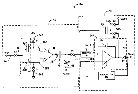
Because switches 50A and 50B are responsive to 01 and 02, respectively, and
couple feedback capacitor 46 to Vref/2 and the output of amplifier 17,
respectively,
the total signal chain gain A between the input of amplifier 15 and the output
of
amplifier 17 is therefore:
A = 2*Vref*[(dC/G)/(Ctot)J*Ai,a*Cs/Cfb,
where A is the gain, Vref is the reference voltage, dC/G is the change in
capacitance per G of acceleration, Ctot is the total capacitance of the
sensor, Aina
is the gain of differential amplifier 15, Cs is the capacitance of sampling
capacitor
34, and Cfb is the capacitance of feedback capacitor 44. For a ratio of sense
capacitor 34 to feedback capacitor 46 (Cs/Cfb) of 1.1, this may yield a net
transduction ratio of approximately. I OOmV/G at the output of the signal
chain.
[0095] In the circuit of FIG 4, capacitive interface circuit 14 includes
differential
amplifier 15, sampling capacitor 34, and a correlated triple sampling circuit
that
reduces one or more noise components in the output signal. In the example of
FIG.
4, the correlated triple sampling circuit is formed by switches 42, 43, 36A,
36B,
and 33, which operate according to different clock phases to implement the
correlated triple sampling process with respect to the signal received by
sampling
capacitor 34. As discussed above, the'correlated tripling sampling circuit
couples
an output of sampling capacitor 34 during a first clock phase (D 1, couples
the first
and second inputs of differential amplifier 15 to ground during a first
(reset)
portion (D I' of the first clock phase, decouples the first and second inputs
of
differential amplifier 15 from ground during a second portion of the first
clock
phase 01, decouples the output of the sampling capacitor 34 from ground during
a
second clock phase 02, couples the first and second capacitive sensor elements
20A, 20B to a reference voltage during the second clock phase 02, and
decouples
the first and second capacitive sensor elements 20A, 20B from the reference
voltage during the first clock phase 01.
[0096] In this manner, sampling capacitor 34 receives one or more noise
components during both the second portion of the first clock phase tD1 and the
second clock phase 02, and blocks at least a portion of the one of more noise
28
CA 02664862 2009-03-27
WO 2008/042015 PCT/US2007/009851
components during the second clock phase 02 to reduce the one or more noise
components in the output signal. In particular, because the noise components
do
not change between the first and second clock phases, capacitor 34 does not
pass
them to selector 56 via switch 43. Instead, the unchanging noise components
are
filtered out of the output signal by the correlated triple sampling process.
In this
way, circuit 14 can reduce kT/C noise, amplifier offset, and flicker noise in
the
output signal applied to ping-pong demodulator 16. The correlated triple
sampling
circuit controls inputs to the differential amplifier 15 such that the
differential
amplifier amplifies the one or more noise components in at least a portion of
the
first clock phase (D1, and amplifies the sensor signal with the one or more
noise
components during the second clock phase (2.
[0097] In the example of FIG. 4, the' correlated triple sampling circuit 14
comprises a first switch 42 that couples an output of sampling capacitor 34 to
ground during the first clock phase c151, and decouples the output of the
sampling
capacitor from ground during the second clock phase (I)2, a second switch 36A
that
couples the first input of the amplifier 15 to ground during the first portion
c1) 1' of
the first clock phase c1 1 and decouples the first input of the amplifier 15
from
ground during a second portion of the first clock phase (I)1, a third switch
36B that
couples the second input of the amplifier 15 to ground during the first
portion (1 1'
of the first clock phase (Ii 1 and decouples the second input of the amplifier
from
ground during a second portion of the first clock phase (D I, and a fourth
switch 33
that couples a reference voltage to the first and second capacitive sensor
elements
20A, 20B during the second clock phase c12 and decouples the reference voltage
from the first and second capacitive sensor elements during the first clock
phase
(1. A fifth switch 43 couples the output of capacitor 34 to selector 56.
[0098] FIG. 5 is a circuit diagram illustrating another example implementation
of
one of interface circuits 12 that is referred to in this disclosure as
interface circuit
12B. Similar to interface circuit 12A, interface circuit 12B in FIG 5 includes
triple
correlated sampler 14 and ping pong demodulator 16. Accordingly, interface
circuit 12A and interface circuit 12B operate in a similar manner with respect
to
correlated triple sampler 14 and ping pong demodulator 16. However, the analog
29
CA 02664862 2009-03-27
WO 2008/042015 PCT/US2007/009851
feedback to the output of correlated triple sampler 14 associated with
interface
circuit 12A is replaced with global analog feedback in interface circuit 12B.
[00991 In FIG. 5, interface circuit 12B interfaces with sensor 4, which
includes
sense capacitors 20A and 20B and excitation capacitors 64A and 64B
(collectively
referred to as "excitation capacitors 64"). Each of sense capacitors 20 has
one of
its capacitive plates tied to a system ground and the other plate coupled to a
corresponding one of excitation capacitors 64. Holding one of the capacitive
plates
of sense capacitors 20 at a common potential is characteristic of pressure
sensors.
Thus, interface circuit 12B of FIG. 5 may be particularly useful for a MEMS
sensor
with pressure sensor architectures.
[01001 In the illustrated example of FIG. 5, the global feedback includes two
feedback paths that provide differential global feedback to respective signal
paths
in sensor 4. The upper feedback path shown in FIG. 5 includes feedback
capacitor
60A which is coupled at one end to a node shared with excitation capacitor 64A
and sense capacitor 20A. At the other end, feedback capacitor 60A is coupled
to
ground or a reference potential via switch 61B and to the output of ping pong
demodulator 16' via switch 61 A. Switches 61 B and 61 A are controlled by
timing
signals (1)2 and 01, respectively.
[01011 Similarly, the lower feedback path in FICA 5 includes feedback
capacitor
60B. Feedback capacitor 60B is coupled at one end to a node shared with
excitation capacitor 64B and sense capacitor 20B. At the other end, feedback
capacitor 60B is coupled to ground *or a reference potential via switch 63A
and to
the output of ping pong demodulator 16 via switch 63B. Switches 63A and 63B
are controlled by timing signals '1 and (2, respectively. The phasing of
switches
63A and 63B is set to provide differential feedback from a single-ended
measurement.
= [01021 In general, the global feedback provided by feedback capacitors 60
linearizes the output of interface circuit 12B (Vout). The net transfer
function for
interface circuit 12B is provided in Equation 1, where Vdr is the amplitude of
(2
that excites capacitors 64, Ccm is the capacitance of capacitors 64, Cfb is
the
capacitance of feedback capacitors 60, Csl is the capacitor of sense capacitor
20A,
and Cs2 is the capacitance of sense capacitor 20B.
CA 02664862 2009-03-27
WO 2008/042015 PCT/US2007/009851
Vout=Vdr(Ccm/Cfb)(Csl-Cs2)[1+2((Ccm+Cfb) /(Csl-Cs2))] (1)
[01031 The 11+2((Ccm+Cfh)/(Csl-Cs2))] component in Equation 1 is non-
linear. This non-linear component may be small for applications such as
posture,
movement, and fall detection. Thus, the bandwidth of interface circuit 12B is
set
by the first-order integration path, i.e., the capacitance of hold capacitor
48
associated with output stage 54A and the corresponding hold capacitor
associated
with output stage 54B. In addition, the accuracy for interface circuit 12B is
set by
the ratio of excitation capacitors 64 and feedback capacitors 60 and the
characteristics of sensor 4.
[01041 FIG. 6 is a circuit diagram illustrating yet another example
implementation
of interface circuits 12 that is referred to in this disclosure as interface
circuit 12C.
Similar to interface circuit 12B, interface circuit 12C is coupled to sensor 4
and
includes triple correlated sampler 14. However, interface circuit 12C replaces
ping
pong demodulator 16 with ping pong demodulator 16B, which outputs a discrete
signal that is applied to sensor 4 as differential global feedback.
[01051 In FIG. 6, correlated triple sampler 14 operates as previously
described.
That is, correlated triple sampler 14 outputs a low noise signal that is
sampled from
sensor 4'. Ping pong demodulator 16B and, more particularly, output stages 54
process the low noise signal as previously described to produce a stable, low
noise
signal that is received by quantizer 56. In FIG. 6, quantizer 56 is clocked
with
timing signal <D I and converts the analog output of output stages 54 into a
digital
bitstream of discrete pulses with amplitude Vref. The digital bitstream
produced
by quantizer 56, i.e., VoutDisc, on average, represents the analog signal
produced
by output stages 54. In this way, the integrators in output stages 54 and
quantizer
56 operate similar to a sigma-delta converter. A digital signal processor or
other
equivalent circuitry quantizer 56 averages the digital bitstream to generate
the
output signal VoutDisc as the average of the discrete pulses.
[0106] The discrete output VoutDisc,is applied as global feedback to sensor 4
through feedback capacitors 60. The global feedback is provided in a similar
31
CA 02664862 2009-03-27
WO 2008/042015 PCT/US2007/009851
fashion as the analog global feedback in FIG. 5. Accordingly, the global
feedback
provided by feedback capacitors 60 linearizes the output of sensor 4 such that
the
net transfer function is provided in equation 2 below, where VoutDisc is the
amplitude of the discrete global feedback that excites capacitors 64, Ccm is
the
capacitance of capacitors 64, Cfb is the capacitance of feedback capacitors
60, Csl
is the capacitor of sense capacitor 20A, and Cs2 is the capacitance of sense
capacitor 20B.
Vout=VoutDisc(Ccm/Cfb)(Csl-Cs2)[1+2((Ccm+Cfb)/(Csl-Cs2))] (2)
[0107] Similar to interface 12B in FIG. 5, the bandwidth of integrator circuit
12C
is set by the first-order integration path and accuracy is set by the ratio of
excitation capacitors 64 and feedback capacitors 60 and the characteristics of
sensor 4.
[01081 FIG 7 illustrates an example circuit diagram for ping-pong demodulator
16.
In general, ping-pong demodulator 1:6 serves as both a demodulator and as an
output sample-and-hold buffer. As previously described, ping pong demodulator
16 includes two interleaved output stages, i.e., output stages 54A and 54B in
FIGS.
4-6. While one of the stages (ping stage) samples the output from correlated
triple
sampler 14 and holds the sampled data until the next clock cycle, the other
stage
(pong stage) presents the previously sampled output of correlated triple
sampler 14
to the output. The pong stage presents the signal sampled during the previous
clock cycle to the output after the signal has settled. In this manner, ping
pong
demodulator 16 substantially reduces clock transients in the output.
[0109] In FIG 7, ping pong demodulator 16 is illustrated in greater detail.
That is,
example components that may be used to realize output stages 54A, 54B are
shown. With respect to FIG. 7, the output from correlated triple sampler 14 is
applied to one side of sampling capacitor 34 while the other side of sampling
capacitor is toggled between a reference voltage and the input of selector 56
by
switches 42 and 43, respectively. The-reference voltage may be equivalent to
Vref/2 as previously described and is provided in FIG. 7 by current source 122
and
transistor 120. The phasing of timing signals c1 and (D2 removes kT/C noise,
32
CA 02664862 2009-03-27
WO 2008/042015 PCT/US2007/009851
amplifier offset, and flicker noise from the signal sampled onto sampling
capacitor
34 during (2.
[0110] When (D2 is high, switch 43 closes and applies the low noise signal
held on
sampling capacitor 34 to selector 56. As shown in FIG. 7, selector 56 may be a
multiplexer 110 that applies the signal at its input to one of output nodes 57
under
the control of timing signal I. For example, when I is high, multiplexer 110
may
apply the low noise signal at its input to output node 57A which is coupled to
output stage 54A. When I is low, however, multiplexer 110 applies the low
noise
signal at its output to output node 57B, which is coupled to output stage 54B.
The
phasing of timing signal I causes multiplexer 110 to alternately apply the low
noise
signal held on sampling capacitor 34 to output stages 54A and 54B for each
clock
cycle of the master clock signal.
[0111] Each of output stages 54 includes a sample-and-hold (S/H) circuit. In
FIG.
7, the S/H circuit of output stage 54A includes transistor 117 and hold
capacitor 48
and the S/H circuit of output stage 54B includes transistor 119 and hold
capacitor
118. This configuration allows for rail-to-rail swing on the output.
Transistors 117
and 119 and hold capacitors 48 and 118 should be well matched. The gate and
source of transistor 117 are coupled to output node 57A and current source
126,
respectively. Similarly, the gate and source of transistor 119 are coupled to
output
node 57B and current source 128. The drain of transistors 117 and 119 is
coupled
to one side of output capacitor 124. The other side of capacitor 124 is
coupled to
the output of ping pong demodulator' 16'.
[0112] The signals produced by output stages 54A, 54B are coupled to
multiplexers 112 and 114, respectively, which are controlled by timing signals
cD3
and (D3', respectively. Multiplexers -112 and 114 selectively apply one of the
signals at its input to its output. When (D3 is high and (D3' is low, for
example,
multiplexer 110 may apply the signal on sampling capacitor 34 to output stage
54A. Accordingly, transistor 117 and hold capacitor 48 in output stage 54A
operate as an integrator to hold this signal. At the same time, multiplexer
112
applies the signal produced by output stage 54B as feedback through feedback
capacitor 46. Also, at the same time, multiplexer 114 applies the signal
produced
by output stage 54B to the output of ping pong demodulator 16 as Vout. As
33
CA 02664862 2009-03-27
WO 2008/042015 PCT/US2007/009851
previously described, the signal produced by output stage 54B at this time is
based
on the signal sampled onto sampling capacitor 34 during the previous clock
cycle.
When the signal was sampled during the previous clock cycle, the signal
included
transients (glitches) due to fast dynamics in the signal path. When this
signal is
applied to the output of ping pong demodulator 16 by multiplexer 114 in the
following clock cycle, the transients have settled, thereby producing a
stable, low
noise signal at the output of ping pong demodulator 16. When c1)3 is low and
(3'
is high, output stage 54A becomes active. In particular, multiplexer 110
applies
the output of capacitor 34 to output stage 54B, multiplexer 112 applies the
signal
produced by output stage 54A as a feedback signal, and multiplexer 114 applies
the signal produced by output stage 54A to the output of ping-pong demodulator
16 as Vout.
[0113] FIG. 8 illustrates timing signals or waveforms for the interface
circuit.
Timing waveforms, 01 130, (151' 132, and (1)2 134, drive the three-step CTS
process for removing kT/C noise from the signal chain. Timing waveforms cp3
136 and c1)3' 138 control operation of ping pong demodulator 16. The phasing
of
timing waveforms 11)1 130, (DI' 132, and (2 134, 03 136, and (D3'138 is
important for proper operation of the interface circuit described in this
disclosure.
However, the exact timing shown in FIG. 8 is presented for purposes of
illustration
and should not be considered limiting.
[0114] FIG. 8 shows that timing waveform (D1' 132 and timing waveform 130 rise
at the same time, but the interval of time that 0 1' 132 is high is shorter
than the
interval of time during which (I)1 130 is high. In addition, FIG. 8 shows that
timing waveform (1 130 falls at the same time that 02 134 rises.
101151 With respect to timing waveforms 03 136 and (153' 138, FIG. 8 shows
that
these waveforms each have a period that is twice the size of the period of
timing
waveform 12 134. In particular, the interval during which timing waveforms
03136 and 03' 138 are high coincide with intervals during which timing
waveform 02 is high. However, the intervals during which timing waveforms 03
136 and 11)3' 138 are high coincide with every other interval for timing
waveform
1152 134.
34
CA 02664862 2009-03-27
WO 2008/042015 PCT/US2007/009851
[01161 FIG 9 illustrates an example circuit diagram for differential amplifier
15 in
correlated triple sampler 14. In general, differential amplifier 15 may be a
low-
power instrumentation amplifier with stable gain characteristics, good
linearity,
e.g., less than 2% integrated non-linearity (INL) +/-20mV, and wide common-
mode range. In the example of FIG. 9, differential amplifier 15 includes field
effect transistors (FETs) 140A, 140B, 142A, 142B, 160, 161, 162, 163, 164 and
165, constant current sources 152, 154, 156, and 158, resistor 144, and
resistors
150A and 150B coupled at output node 146. The gates of FETS 140A, 140B
receive bias voltages Vb. Current sources 152, 154 generate bias currents Ibl,
and
current sources 156, 158 generate bias currents Ibo. The gates of FETs 140A,
140B receive the differential input signal from the sensor, e.g., from
variable
capacitors 20A, 20B. Resistor 144 is coupled across the sources of FETs 140A,
140B and across the drains of FETs 160, 161. Current through front-end field
effect transistors (FETs) 142A and 142B is held constant by a mirror servo
loop.
The mirror servo loop forces the differential voltage received at the gates of
input
FETs 140A and 140B to fall across source resistor 144. Top-side currents,
i.e.,
currents generated by current sources 152 and 154, are mirrored to an output
resistor tap 146 via FETs 162, 163, 164, 165. In particular, the gate of FET
162 is
coupled to current source 154 and the gate of FET 163 is coupled to the gate
of
FET 160. Differential amplifier 15 has a gain that is set by the resistor
ratio
Ro/Ri, where Ro is the resistance of each of resistors 150A and 150B and Ri is
the
resistance of source resistor 144. This gain may be stable across process
corners.
Additionally, by supplying a reference (Vref) to the top of the resistor
string, i.e.,
resistor 150A, an arbitrary bias point for the output, Vout sense, can be set.
For
example, a reference voltage of 1.2V may yield a sensor centered at 0.6V.
Other
features of differential amplifier 15 may include improved linearity over the
dynamic range of the sensor, e.g., +/- 20mV, a wide common-mode range such as
0 V to approximately 1.2V, and an inherent ability to bootstrap pads and other
critical signal lines through a low-impedance source, which servo tracks the
gate
voltage.
[01171 A sensor device as described in this disclosure, as well as associated
circuitry, devices, systems and methods, may be useful in a variety of
applications,
CA 02664862 2009-03-27
WO 2008/042015 PCT/US2007/009851
For example, the invention may be applied to support sensing relating to
electrical
stimulation or drug delivery therapies for a variety of symptoms or conditions
such
as cardiac arrhythmia, cardiac fibrillation, chronic pain, tremor, Parkinson's
disease, epilepsy, urinary or fecal incontinence, sexual dysfunction, obesity,
or
gastroparesis, and may apply to electrical stimulation or drug delivery to a
variety
of tissue sites, such as the heart, brain, spinal cord, pelvic nerves,
peripheral
nerves, or the gastrointestinal tract of a patient.
[01181 Sensor device 2 may be integrated with, housed in, coupled to, or
otherwise
associated with an external or implantable medical device, such as a
cardioverter/defibrillator, spinal cord stimulator, pelvic nerve stimulator,
deep
brain stimulator, gastrointestinal stimulator, peripheral nerve stimulator, or
muscle
stimulator. Sensor device 2 also may be used in conjunction with implantable
or
external drug delivery devices. For example, sensor device 2 may reside within
an
implantable medical device housing or a lead or catheter coupled to such a
device.
Sensor device 2 may be used in conjunction with different therapeutic
applications,
such as cardiac stimulation, deep brain stimulation (DBS), spinal cord
stimulation
(SCS), pelvic stimulation for pelvic pain, incontinence, or sexual
dysfunction,
gastric stimulation for gastroparesis, obesity or other disorders, or
peripheral nerve
stimulation for pain management. Stimulation also may be used for muscle
stimulation, e.g., functional electrical stimulation (FES) to promote muscle
movement or prevent atrophy.
[01191 The illustrated components of sensor device 2 and sensor interface 6
may
be realized by any of a variety of different fabrication techniques, including
various IC process technologies such as complementary metal oxide
semiconductor (CMOS), bipolar junction transistor (BJT), bipolar-CMOS
(BiCMOS), silicon germanium (SiGe), gallium arsenide (GaAs), and the like. In
addition, operation of sensor device 2 may be implemented in part or aided by
additional components or functionality realized by one or more DSPs,
microprocessors, application specific integrated circuits (ASICs), field
programmable gate array (FPGAs), or any other equivalent integrated or
discrete
circuitry, as well as any combination of such components.
36