Note: Descriptions are shown in the official language in which they were submitted.
CA 02665047 2009-03-27
WO 2008/042859 PCT/US2007/080104
DESCRIPTION
METHOD AND APPARATUS FOR INFRARED DETECTION AND DISPLAY
Cross-Reference to Related Applications
The present application claims the benefit of U.S. Application Serial No.
60/930,225,
filed May 14, 2007, and claims the benefit of U.S. Application Serial No.
60/848,581, filed
September 29, 2006, both of which are hereby incorporated by reference herein
in their
entirety, including any figures, tables, or drawings.
Background of Invention
There are many applications for detecting infrared (IR) radiation. IR can
refer to
radiation having wavelengths longer than visible light (> 0.7 m) up to about
14 q.m, with
near-IR being a subset referring to wavelengths from about 0.7 m to about 1.0
m. One
application is the detection of IR in environments with low ambient light,
which can occur,
for example, at night. It can also be useful to display to a user the image of
the detected IR at
a wavelength visible to the user. One common device for detecting IR images
and displaying
the detected images to a user is night-vision goggles.
Conventional night vision goggles are complex electro-optical devices that can
require very high operating voltages and cost thousands of dollars. Typical
night vision
goggles intensify existing light instead of relying on their own light source
and are sensitive
to a broad spectrum of light, from visible through infrared. A conventional
lens, called the
objective lens, captures ambient light, including some near-infrared light.
The gathered light
is then sent to an image-intensifier tube. The tube outputs a high voltage,
e.g., about 5,000
volts, to the image-tube components. The image-intensifier tube has a photo
cathode, which
is used to convert the photons of light energy into electrons. As the
electrons pass through the
tube, similar electrons are released from atoms in the tube, multiplying the
original number of
electrons by a factor of thousands through the use of a micro channel plate
(MCP) in the tube.
When the electrons from the photo cathode hit the first electrode of the MCP,
they are
accelerated into the glass micro channels by the 5,000-V bursts being sent
between the
electrode pair. As electrons pass through the micro channels, they cause
thousands of other
electrons to be released in each channel using a process called cascaded
secondary emission.
These new electrons also collide with other atoms, creating a chain reaction
that results in
CA 02665047 2009-03-27
WO 2008/042859 PCT/US2007/080104
2
thousands of electrons leaving the channel where only a few entered. At the
end of the image-
intensifier tube, the electrons hit a screen coated with phosphors. These
electrons maintain
their position in relation to the channel they passed through, which provides
a perfect image
since the electrons stay in the same alignment as the original photons. The
energy of the
electrons causes the phosphors to reach an excited state and release photons.
These phosphors
create the green image on the screen that has come to characterize night
vision. The green
phosphor image is viewed through another lens called the ocular lens, which
allows you to
magnify and focus the image. The night vision device may be connected to an
electronic
display, such as a monitor, or the image may be viewed directly through the
ocular lens.
Accordingly, there is a need for IR sensors/detectors, and IR sensor/detector-
display
combinations, that operate at low operating voltages and are lightweight and
cost-effective to
produce.
Brief Summary
Embodiments of the subject invention relate to a method and apparatus for
infrared
(IR) detection. A specific embodiment utilizes organic layers to produce a
phototransistor for
the detection of IR radiation. The wavelength range of the IR detector can be
modified by
incorporating materials sensitive to photons of different wavelengths. In a
specific
embodiment, quantum dots of materials sensitive to photons of different
wavelengths than the
host organic material of the absorbing layer of the phototransistor can be
incorporated into
the absorbing layer so as to enhance the absorption of photons having
wavelengths associated
with the material of the quantum dots.
In another embodiment, a photoconductor structure can be used instead of a
phototransistor. In one embodiment, the photoconductor can incorporate PbSe or
PbS
quantum dots. In another embodiment, the photoconductor can incorporate
organic materials.
Specific embodiments also involve displaying a detected IR image to a user. In
a
specific embodiment, organic materials can be used to create an organic light-
emitting
device. Additional material that emits at different wavelengths can be added
to the light-
emitting layer. In a specific embodiment, quantum dots of materials associated
with emission
of photons of different wavelengths than the host organic material of the
emission layer can
be incorporated into the emission layer to enhance the output display of the
organic light-
emitting device to the user. In a preferred embodiment, the IR detection is
accomplished
with a phototransistor and the displaying of the detected IR image is
accomplished with an
CA 02665047 2009-03-27
WO 2008/042859 PCT/US2007/080104
3
organic light-emitting device such as an organic light-emitting diode (OLED).
In a more
preferred embodiment, the phototransistor and OLED are in series.
Embodiments of the subject invention pertain to a method and apparatus for
night
vision. In an embodiment, a night vision device can be accomplished by the
deposition of
layers of organic thin films. Embodiments of the subject device can operate at
low operating
voltages, such as 10-15 V. In addition, the cost of manufacturing specific
embodiments of
the subject device can be lower than the cost of manufacturing conventional
night vision
systems. In an embodiment of the subject night vision device an organic
phototransistor can
be in series with an organic light-emitting device, such as an organic light-
emitting diode
(OLED).
Brief Description of Drawings
Figure 1 shows an embodiment of a two-dimensional infrared image
sensor/detector,
a two-dimensional infrared image sensor/display array without pixelation, and
a circuit model
of the sensor/display array.
Figure 2 shows a PNP bipolar phototransistor and an NPN bipolar
phototransistor in
accordance with embodiments of the subject invention.
Figure 3 shows an embodiment of an infrared image/sensor display array using
PbSe
quantum dots in the absorption layer.
Figure 4 shows an embodiment of the subject display device incorporating CdSe
quantum dots in the emission layer.
Figure 5 shows materials that can be used in various embodiments of the
subject
invention.
Figure 6 shows an embodiment using PbSe quantum dots as photoconductors.
Figure 7 shows an embodiment using organic materials as the photoconductors.
Figure 8 shows an embodiment using a photoconductor as a light sensor.
Detailed Disclosure
Embodiments of the subject invention relate to a method and apparatus for
infrared
(IR) detection. A specific embodiment utilizes organic layers to produce a
phototransistor for
the detection of IR radiation. The wavelength range of the IR detector can be
modified by
incorporating materials sensitive to photons of different wavelengths. In a
specific
embodiment, quantum dots of materials sensitive to photons of different
wavelengths than the
CA 02665047 2009-03-27
WO 2008/042859 PCT/US2007/080104
4
host organic material of the absorbing layer of the phototransistor can be
incorporated into
the absorbing layer so as to enhance the absorption of photons having
wavelengths associated
with the material of the quantum dots.
In another embodiment, a photoconductor structure can be used instead of a
phototransistor. In one embodiment, the photoconductor can incorporate PbSe or
PbS
quantum dots. In another embodiment, the photoconductor can incorporate
organic materials.
Specific embodiments also involve displaying a detected IR image to a user. In
a
specific embodiment, organic materials can be used to create an organic light-
emitting
device. Additional material that emits at different wavelengths can be added
to the light-
emitting layer. In a specific embodiment, quantum dots of materials associated
with emission
of photons of different wavelengths than the host organic material of the
emission layer can
be incorporated into the emission layer to enhance the output display of the
organic light-
emitting device to the user. In a preferred embodiment, the IR detection is
accomplished
with a phototransistor and the displaying of the detected IR image is
accomplished with an
organic light-emitting device such as an organic light-emitting diode (OLED).
In a more
preferred embodiment, the phototransistor and OLED are in series.
Embodiments of the subject invention pertain to a method and apparatus for
night
vision. In an embodiment, a night vision device can be accomplished by the
deposition of
layers of organic thin films. Embodiments of the subject device can operate at
low operating
voltages, such as 10-15 V. In addition, the cost of manufacturing specific
embodiments of
the subject device can be lower than the cost of manufacturing conventional
night vision
systems. In an embodiment of the subject night vision device an organic
phototransistor can
be in series with an organic light-emitting device, such as an organic light-
emitting diode
(OLED).
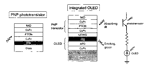
Preferably, electrodes that are transparent to infrared light are used to
allow IR
radiation to enter the phototransistor. A schematic diagram of an embodiment
of an IR
sensor/detector, an embodiment of an IR sensor-display combination, and a
circuit model for
the IR sensor-display combination are shown in Figure 1. A PNP bipolar
phototransistor
created using layers of organic material is shown on the left of Figure 1.
Here, CuPc is the n-
layer and PTCBI is the p-layer. Although the curved arrow symbolizing light
(absorbing IR
and emitting green) are shown pointing to the absorption layer and emission
layer,
respectively, the IR light enters from the top and the visible light is
emitted from the bottom
of the device shown in Figure 1. In the middle of Figure 1, the integration of
the
CA 02665047 2009-03-27
WO 2008/042859 PCT/US2007/080104
phototransistor shown on the left with an OLED is shown. IR images can be
incident on the
top of the electrode layer (NiO) of the phototransistor and pass through the
CuPc layer and
into the absorption layer (PTCBI).
Upon photoexcitation with infrared light, charge carriers are generated in the
5 phototransistor and injected into the OLED, which then generates photons in
the visible
range. Because of the low conductivity of organic thin films, the electric
field will be
confined within the photoexcited area and visible photons will be generated
within the
excited area. As a result, if a broad area device is exposed to an infrared
image, a visible
image will be generated. Preferably, an electrode transparent to visible light
is used at the
bottom, where the output image is emitted. In the embodiment shown, ITO is
used as an
electrode, which is transparent to visible light. Other materials can also be
used. A circuit
diagram of the integrated device shown in the middle is shown on the right
side of Figure 1.
In a specific embodiment, no electronics are required to operate the device.
In an
embodiment, the operating voltages of the phototransistor and the light-
emitting device are
less than 10 V, such that the total operating voltages can be less than 20 V.
This device can
be made very light weight.
In an embodiment, glass can be used as a substrate for fabrication. The entire
phototransistor and OLED combination can be very thin, for example, less than
1[Im. The
glass substrate with the thin layer can then be made part of night vision
goggles where the
thin layer is positioned to receive an IR image and a user is positioned to
see the visible
image emitted from the glass, or plastic, substrate.
Figure 2 shows the PNP bipolar transistor of Figure 1 and an NPN
phototransistor,
which can also be utilized in accordance with the subject invention.
The fabrication procedure for a specific embodiment of the subject IR detector-
display combination will now be described. This fabrication procedure does not
require any
patterning. Other fabrication techniques, as well as other materials, as would
be apparent to
one skilled in the art having the benefit of the subject disclosure, can also
be utilized in
accordance with the subject invention. Devices are grown on a glass substrate
or plastic
substrate precoated with a 100 nm thick layer of indium-tin-oxide having a
sheet resistance of
20 ohms/square. Substrates are degreased with solvents and then cleaned by
exposure to
oxygen plasma and UV-ozone ambient. All layers are vacuum deposited grown in
succession
without breaking the vacuuin. In the first deposition step on top of the
indium-tin-oxide
(ITO) layer, to fabricate the integrated PNP phototransistor and OLED shown in
the middle
CA 02665047 2009-03-27
WO 2008/042859 PCT/US2007/080104
6
of Figure 1, a 10-nm-thick CuPc is deposited as a hole injection layer. A 50
nm-thick NPD
layer is then grown and acts as a hole transport layer. Next, a 60 nm-thick
Alq3 emissive
layer is deposited. A LiF(2 nm)/NiO (10nm) charge generation layer is then
deposited. This
results in an OLED. To fabricate the phototransistor on the top of the light
emitting device, a
40 nm thick CuPc layer, a 50 mn thick PTCBI layer, a 40 nm thick CuPc layer,
and a 1000
nm NiO layer are then deposited.
In another specific embodiment, referring to Figure 3, the PTCBI layer of the
phototransistor is replaced with a PbS or PbSe quantum dot layer. The PbS or
PbSe absorbs
photons of different wavelengths than the PTCBI layer. As an example, a PTCBI
layer can
be created that absorbs photons up to wavelengths of about 1 m and a PbSe
quantum dot
layer, or PbS quantum dot layer, can be created that also absorbs photons
having wavelengths
in the range of about 1 m to about 3 m, so as to expand to wavelength range
for detection.
Other wavelength ranges can be accomplished by proper selection of the
material in the
absorption layer.
In a further specific embodiment, referring to Figure 4, the 60 nm Alq3 layer
of the
light emitting device from Figure 1 or Figure 3 is replaced with a 50 nm Alq3
layer and a
CdSe quantum dot layer. The material for the quantum dot layer can facilitate
emission of
light at wavelengths different from the light emitted by the Alq3 layer.
Accordingly, other
materials can also be utilized in accordance with the subject invention.
Figure 5 shows structures of materials that can be utilized with embodiments
of the
subject invention. Shown in Figure 5 are structures for tris-(8-
hydroxyquinoline) aluminum
(Alq3), 4-4'-bis[N-(1-naphthyl)-N-phenyl-amino]biphenyl (NPD), copper
phthalocyanine
(CuPc), and perylene-3,4! 8,10-tetra-carboxylic-diimide-di-2,6-isopropy-phenyl
(PTCDI).
Although exemplary embodiments directed to a phototransistor and
phototransistor/OLED combination fabricated primarily from organic material
layers have
been described, additional embodiments can utilize inorganic materials for the
phototransistor
and/or the light emitting device. Examples of inorganic materials that can be
used to
fabricate phototransistors and/or light emitting device in accordance with the
subject
invention include, but are not limited to, amorphous silicon, germanium, and
diamond-like
carbon. Thin film amorphous silicon could have PbSe or PbS to absorb IR. An
inorganic
OLED can use ZnO to emit visible light. The use of inorganic materials in the
absorption
layer can allow detection of IR with wavelengths in the range of about 1 m to
4 m. These
materials and the techniques to fabricate phototransistors and/or OLED's with
structures
CA 02665047 2009-03-27
WO 2008/042859 PCT/US2007/080104
7
similar to those shown in Figures 1, 2, 3, and 4 are known to those skilled in
the art. In this
way, an inorganic phototransistor can be incorporated with an organic OLED and
an organic
phototransistor can be incorporated with an inorganic OLED.
Embodiments of the present invention can incorporate a photoconductor. In
specific
embodiments, a photoconductor can replace the phototransistor described in the
above
embodiments. Figure 6 shows a photoconductor device incorporating PbSe quantum
dots.
The PbSe quantum dots can be used to sense photons with wavelengths between 1
m to 3
m. The photoconductor structure can be formed of photoconductive material
arranged
between two electrodes. In one embodiment, one electrode can be fo_rmed of
gold (Au) and
the second electrode can be formed of ITO. In an embodiment, PbS quantum dots
can be
used in the place of the PbSe quantum dot layer. In operation, carriers can be
photoexcited in
the quantum dot (QD) layer through the absorption of IR rays. The carriers can
travel to an
OLED element to emit, for example, green light. In particular, electrons may
be injected into
an emissive layer of the OLED element and recombine with holes to give off
light.
In the embodiment shown in Figure 6, the photoconductor can be formed on an
OLED element. The OLED element can be formed on a glass substrate and can
incorporate
an ITO layer formed on the substrate, a CuPc layer formed on the ITO layer to
act as a hole
transport layer, a NPD layer formed on the CuPc layer to act as a hole
transport layer, an Alq
layer formed on the NPD layer, and a LiF/NiO layer for charge generation
formed on the Alq
layer. The photoconductor can be formed on the LiF/NiO layer by depositing a
gold layer on
the LiF/NiO layer, forming a photoconductive material layer on the gold layer,
and forming
an ITO layer on the photoconductive material layer.
Figure 7 shows a photoconductor device incorporating organic materials.
Referring to
Figure 7, one of the electrodes for the photoconductor can be eliminated when
incorporated
with an OLED element. In particular, the photoconductive material can be in
direct contact
with a hole transporting layer of an OLED. In an embodiment, titanyl
phthalocyanine
(TiOPc) can be used as the photoconductive material of a photoconductor
device. The TiOPc
can respond to IR rays because TiOPc absorbs wavelengths at 0.8 m. The OLED
element
can be formed on a glass substrate and can include an ITO layer formed on the
substrate, a
LiF/NiO layer formed on the ITO layer, an Alq layer formed on the LiF/NiO
layer and a NPD
layer formed on the Alq Layer. The photoconductive material can be formed
directly on the
NPD layer without an intervening electrode.
CA 02665047 2009-03-27
WO 2008/042859 PCT/US2007/080104
8
Figure 8 shows an embodiment incorporating a photoconductor as the light
sensor. A
photoconductor can have very large gain or amplification and is ideal to
amplify the signal.
The photoconductor device includes two layers, a charge transport layer and a
sensitizer.
NPD can be used as a charge transport layer and PbSe, PbS, and/or InAs quantum
dots can be
utilized for photon absorption.
In operation, carriers can be photoexcited in the TiOPc layer. The carriers
can travel
to the OLED element to emit, for example, green light. In particular, holes
can be injected
into the NPD layer to recombine with electrons and give off light.
In embodiments of the present invention, the gain in photoconductors can be as
large
as 100,000.
For embodiments incorporating photoconductors instead of phototransistors,
fabrication may involve less process steps due to embodiments of
photoconductors being
single layer devices instead of a three-layer NPN or PNP structure.
All patents, patent applications, provisional applications, and publications
referred to
or cited herein are incorporated by reference in their entirety, including all
figures and tables,
to the extent they are not inconsistent with the explicit teachings of this
specification.
It should be understood that the examples and einbodiments described herein
are for
illustrative purposes only and that various modifications or changes in light
thereof will be
suggested to persons skilled in the art and are to be included within the
spirit and purview of
this application.