Note: Descriptions are shown in the official language in which they were submitted.
CA 02665431 2009-04-02
WO 2008/041222 PCT/IL2006/001144
PHASED SHIFTED OSCILATOR AND ANTENNA
FIELD OF THE INVENTION
The present invention relates generally to a device and process for sending
and receiving radio wave energy for utilizing information, and more
specifically to
phased array antennas and their application in wireless communication.
BACKGROUND, OF THE INVENTION
Antennas are designed to transmit and receive electro-magnetic waves. A phased
array antenna is an antenna comprising a plurality of radiator elements
(radiators) with a
directive radiation pattern (beam) which can be controlled by controlling
individual
radiator elements (radiators) or groups of radiator elements in the antenna.
In general,
the steering direction of the radiation pattern is deterinined by control of
the phases of
the signal to or from the radiator elements. In conventional phased array
antennas the
phase control is achieved by phase shifters. The specific phases are typically
determined
by a digital signal processing (DSP) subsystem.
One example of phased array antennas is disclosed in U.S. patent application
serial number 6,759,980 disclosing a phased array antenna coinprising an
input, a feed
network electronically coupled to the input, a plurality of radiators, a
plurality of phase
shifters for providing phase shifts for the signals prior to transmitting the
signals to the
radiators or receiving the signals from the radiators, and a controller for
controlling the
phase shift provided by the phase shifters. .
Fig. 1 illustrates a simplified block diagram of a system generally referenced
100
comprising a multiple power divider 140 for distributing the reference signal
101 to one
or more transmitter/receiver (T/R) modules, and a simple phased array antenna
(PAA)
150, known in the art. Fig. 1 illustrates electronically steering the wave
front of a signal.
Three possible wave fronts 162, 164, 166 are shown. Reference signal 101 is
inputted to
the multiple power divider 140. The ;reference signal is normally generated by
a
reference signal generator (not shown in Fig. 1).
1
CA 02665431 2009-04-02
WO 2008/041222 PCT/IL2006/001144
The power divider 140 distributes the reference signal 101 to four phase
shifters
112, 114, 116, 118. The phase shifters 112, 114, 116, 118 provide respective
phase
shifl:s sl, s2, s3, s4 degrees (not shown). The wave front 162, 164, or 166 is
determined
by the phase shifts sl, s2, s3, s4 of the phase shifters. The phased array
antenna 150
comprises phase shifters 112, 114, 116, 118, amplifiers 122, 124, 126, 128,
and
radiators 132, 134, 136, 138. Each of the phase shifl;ers 112, 114, 116 118 is
connected
to an amplifier 122, 124, 126, 128. Each of the amplirers 122, 124, 126, 128
transfers
an amplified and phase shifted signal to a respective radiator. The PAA of
Fig. 1 can
steer the wave front only in one dimension, either an azimuth dimension or an
elevation
1 o dimension.
An exemplary PAA comprises an array of radiators in which the relative phases
of the electromagnetic signals radiated by the radiators are varied in such a
way so as to
cause the radiation pattern of the phased array antenna to be in a desired
direction. In
Fig. 1, numeral 161 illustrates a radiation pattern (beam).
The siinplified phased array antenna 150 illustrated by Fig. 1 typically
comprises
an array of T/R modules 102, 104, 106, 108 and an array of radiators 132, 134,
136,
138. In the architecture of the PAA of Fig. 1, each radiator is connected to
one T/R
module. In Fig. 1 only the transmit part of the T/R modules 102, 104, 106, 108
are
shown.
Exemplary PAAs use transmitters (TR) or receivers (RX) or T/R modules, which
perforin functions, such as, shifting the phase of a signal by a
predeterinined ainount of
degrees. For example T/R module 102 in Fig. 1 phase shifts a signal by s 1
degrees.
An exemplary conventional T/R module 102 comprises among other elements a
phase shifter 112 and an ainplifier 122. Exemplary PAA use a plurality of T/R
modules,
each T/R module comprising a phase shifter (PS). PS are electronic devices
enabling the
antenna beam to be electronically steered, in a desired direction, without
mechanically
repositioning the PAA. Conventional PAA are extremely expensive and of high
power-
consumption, therefore they are mainly used in military applications, such as
aircraft
radars and missile-radars. For instance, in an exemplary PAA, about 4000 phase
shifters
3o are used; each phase shifter costs several thousands U.S. dollars,
resulting in a total cost
2
CA 02665431 2009-04-02
WO 2008/041222 PCT/IL2006/001144
of millions of U.S. dollars for such PAA. There is therefore a need for low
cost phased
array antennas giving about the same performance of the conventional high cost
phased
array antennas.
SUMMARY OF THE INVENTION
An aspect of some embodiments of the invention relates generally to a Phased
Array Antenna ("PAA") system and more specifically for a PAA for use in
wireless or
telecoirununication networks, such as Wi-Fi, Wi-Max, cellular communication,
or
1 o satellite mobile television.
The PAA of this invention is an active phased array antenna. The word active
is
used to emphasize that the PAA is being steered electronically and not
mechanically,
also by using a T/R module for each radiator.
An aspect of some embodiments of the invention relates to a PAA for high
quality video seivices, high speed data' services, Voice over IP (VOIP), or
internet
telephony.An aspect of some embodiments of the invention relates to a new
apparatus
'or circuit called hereinafter a phased shifted injection oscillator (PSIO).
An aspect of some embodiments of the invention relates to a new apparatus or
circuit called hereinafter a phased shifted injection locked push-push
oscillator
(PSIPPO).
An aspect of some embodiments of the. invention relates to a phased array
antenna system comprising of a plurality of PSIOs or a plurality of PSIPPOs.
An aspect of some embodiments of the invention relates to a low cost or an
inexpensive PAA. In exemplary embodiments of the invention, a PAA using a
plurality
of PSIPPOs achieves about the saine or better perforinances, such as higher
efficiency,
as of a conventional PAA system that uses conventional prior art T/R modules
based on
conventional phase shifting circuits.
An aspect of some embodiments of the invention relates to a PAA using a
plurality of PSIPPOs enabling azimuth or elevation beam steering.
An aspect of some embodiments of the invention relates to a PAA using a
plurality of PSIPPOs that generates narrow beams.
3
CA 02665431 2009-04-02
WO 2008/041222 PCT/IL2006/001144
In exemplaiy embodiments of the invention, the narrow beams allow a wider
coverage range or a lower electromagnetic interference than conventional
antenna based
on prior art This eiiables a significant increase in data throughput or
increase in the
numbers of simultaneous users of a wireless network, such as Wi-Fi, Wi-Max,
and other
wireless networks.
In accordance with an exemplary enlbodiment of the invention there is provided
an oscillator comprising a reflection amplifier; a band rejection filter
comprising at least
one variable capacitor and at least one resonator, wherein said band rejection
filter is
connected to said reflection amplifier. In exeinplaiy embodiments of the
invention the
band rejection filter is a two port baiid rejection filter. In exemplary
embodiments of the
invention an input reference signal is injected into the oscillator. In
exemplary
embodiments of the invention the output signal of the oscillator is locked. In
exemplary
embodiments of the invention the oscillator is voltage controlled.
In accordance with an exemplary embodiment of the invention there is provided
an oscillator coinprising a power divider; a time delay unit; a band rejection
filter; at
least two reflection ainplifiers; and a power combiner. In exemplary
embodiments of the
invention the band rejection filter comprises at least two variable capacitors
and at least
two inductors iinpleinenting a resonator. In exemplary embodiments of the
invention the
variable capacitors are voltage controlled by a signal generated by a DSP
unit.
In accordance with an exemplary -embodiment of the invention there is also
provided a phased shifted injection locked push-push oscillator coinprising a
power
divider operative to divide a received reference signal into a first portion
and into a
second portion, the second portion is tiirie delayed by a predetermined amount
of delay
time, relative to the first portion; and a push-push oscillator receiving the
first and
second portions and generating an output signal; wherein the push-push
oscillator
coinprises a band rejection filter adapted to change the phase of the first or
second
portions resulting in an output signal having a phase shifted relative to the
phase of the
reference signal. In exemplary embodiments of the invention the power divider
is a zero
degree power divider. In exeinplary embodiments of the invention the power
divider is a
Wilkinson power divider. In exeinplary embodiments of the invention the
generated
4
CA 02665431 2009-04-02
WO 2008/041222 PCT/IL2006/001144
output signal has stability characteristics about the same as the received
reference
signal. In exemplary embodiments of the invention the generated output signal
has noise
characteristics about the same as the received reference signal. In exemplary
embodiments of the invention the predetermined amount of delay time is of
about half
of the period of the reference signal. In exemplary embodiments of the
invention the
predetermined amount of delay time is an odd multiple of about half of the
period of the
reference signal. In exemplary embodiments of the invention the generated
output signal
has the same frequency and about the saine noise characteristics the received
reference
signal. In exeinplary embodiments of the invention the generated output signal
has
stability characteristics about the same as the received reference signal. In
exemplary
embodiments of the invention the phase shift of the output signal relative to
the received
reference signal is in the range of about -100 to about +100 degrees. In
exemplary
embodiments of the invention the band rejection filter comprises at least two
variable
capacitors. In exemplaiy embodiments of the invention the variable capacitors
are used
for changing the resonant frequency of the band rejection filter.
In accordance with an, exemplary embodiment of the invention there is also
provided a method for phase shifting an injection locked push-push oscillator,
comprising 'dividing a received reference signal into a first portion and into
a second
portion, the second portion is time delayed by a predetermined amount of delay
time,
relative to the first portion; receiving the first and second portions by a
push-push
oscillator; and generating an output signal by the by the push-push
oscillator; wherein
the push-push oscillator is adapted to change the phase of the first or second
portions
resulting in an output signal having a phase shifted relative to the phase of
the reference
signal. In exemplary embodiments of the invention the predetermined amount of
delay
time the second portion is delayed relative to the first portion is about half
the period of
the reference signal. In exemplary embodiments of the invention the
predetermined
amount of time delay the second portion is delayed relative to the first
portion is an odd
multiple of about half the period of the reference signal.
In accordance with an exeinplary embodiment of the invention there is also
provided a transmitter/receiver module comprising at least one level of phased
shifted
5
CA 02665431 2009-04-02
WO 2008/041222 PCT/IL2006/001144
injection locked push-push oscillator; and a receiving functionality receiving
a sainpled
portion of power subsequently handled by the at least one level of phased
shifted
injection locked push-push oscillators
In accordance with an exemplary einbodiment of the invention there is also
proVided a method for phase shifting an injection locked push-push oscillator,
comprising receiving a first signal having a phase; dividing the first signal
and injecting
a first portion of the first signal into a band rejection filter and the
second portion of the
first signal into a time delay unit; changing the resonant frequency of the
first or second
portion of the first signal; oscillating the first portion and the second
portion of the first
signal between the band rejection filter and at least two reflection amplif
ers; coinbing
the first and second portions of the first signal froin the at least two
reflection
ainplifiers; and outputting the combined signal. In exemplary einbodiments of
the
invention the first signal is a reference signal or signal from a previous
phase shifting an
injection locked push-push oscillator. In exemplary embodiments of the
invention the
combined signal is outputted to another phase shifting an injection locked
push-push
oscillator or to a radiator. In exemplary embodiments of the invention the
combined
signal has about twice the frequency and twice the phase shift of the first -
signal. In
exemplary embodiments of the invention the time delay unit creates a time
delay of
about half the period of the first signal.
In accordance with an exeinplary embodiment of the invention there is also
provided a phased array antenna having a steer able aiitenna beam in azimuth
and
elevation the antenna coinprising: a plurality of radiators, amplifiers,
mixers, sampling
couplers and phase shifter injection locked oscillators, said phase shifter
iiijection
locked oscillators are for steering the antenna beam in the elevation and
azimuth
direction. In exemplary embodiments of the invention each of the phased
shifted
injection locked push-push oscillators comprise a power divider operative to
divide a
received reference signal into a first portion and into - a second portion,
the second
portion is time delayed by a predetermined amount of delay time, relative to
the first
portion; and a push-push oscillator receiving the first and second portions
and
generating an output signal; wherein the push-push oscillator comprises a band
rejection
6
CA 02665431 2009-04-02
WO 2008/041222 PCT/IL2006/001144
filter adapted to change the phase of the first or second portions resulting
in an output
signal having a phase shifted relative to the phase of the reference signal.
In exemplary
embodiments of the invention a first portion of the phase shifted injection
locked push-
push oscillators are being phase shifted by a first degree; a second portion
of the phase
shifted injection locked push-push oscillators are being phase shifted by a
second
degree, and a third portion of the phase shifted injection locked push-push
oscillators
are being phase shifted by a third degree, said first degree is relative to
said second
degree is relative to said third degiee. In exemplary embodiments of the
invention the
phased array antenna is used with a wireless communication device. In
exemplaiy
embodiments of the invention the phased array antenna is used with a wireless
access
point. In exemplary embodiments of the invention the phased array antenna is
used with
a satellite mobile television system. In exemplary einbodiinents of the
invention the
phased array antenna is used with a satellite antenna. In exeinplary
einbodiments of the
invention the phased array antenna is used with an antenna connected to a data
switching device. In exemplary embodiments of the invention the phased array
antenna
is used with an antenna connected to a data receiving and transmitting device.
7
CA 02665431 2009-04-02
WO 2008/041222 PCT/IL2006/001144
BRIEF DESCRIPTION OF THE FIGURES
Exeinplary non-limited embodiments of the invention will be described, with
reference to the following description of the embodiments, in conjunction with
the
figures. The figures are generally not shown to scale and any sizes are only
meant to be
exemplary and not necessarily limiting. In the figures, identical structures,
elements or
pai-ts that appear in more than one figure are preferably labeled with a same
or similar
number in all the figures that they appear in.
Fig. 1 illustrates a simplified block diagram of a system comprising a
multiple
power divider and a simple phased array antenna known in the art.
Fig. 2 is a schematic diagram of a phased shifted injection oscillator (PSIO)
,
according to an exemplary embodiment of the invention.
Fig. 3 is a schematic diagram a band rejection filter (BRF) according to an
exemplaiy embodiment of the invention.
Figs. 4, 5 are non-limiting examples illustrating a behavior of a PSIO, in
accordance with exemplary embodiments of the invention.
Fig. 6 is a simplified block diagram illustration of a phased shifted
injection
locked push-push oscillator (PSIPPO), in accordance with an exelnplary
embodiment of
the invention.
Fig. 7 is a schematic diagram of a BRF, according to an exemplary embodiment
of the invention.
Fig. 8A, 8B, 8C, 8D are non-limiting example illustrating a waveform behavior
of a phased shifted injection locked push-push oscillator (PSIPPO), in
accordance with
exeinplary embodiments of the invention.
Fig. 9 illustrates a phased array antenna, able to steer the antenna beam in
azimuth and elevation, in accordance with an exemplary embodiment of the
invention.
Fig. 10 illustrates a wireless networlc system, in accordance with exemplary
embodiments of the invention.
Fig. 11 illustrates a satellite mobile television system in accordance with
exemplary embodiments of the invention.
~
CA 02665431 2009-04-02
WO 2008/041222 PCT/IL2006/001144
DETAILED DESCRIPTION OF EXEMPLARY EMBODIMENTS
This invention describes new and improved phased sllifted injection
oscillator, a
phased shifted injection locked push-push oscillator and a phased array
antennas (PAA).
The PAAs in accordance with an exemplary einbodiinent of the present invention
are
low cost, and therefore can be used in various commercial. applications, such
as wireless
communication or satellite mobile television. The PAAs of the present
invention
provides significant enhancements and improvements over prior art PAA, as will
be
shown from the specifications and figures.
A phased array antenna according to the present invention comprises a
plurality
phase shifting elements and other electronic components. Conventional phase
shifters
are expensive electronic components or are affected by high RF loss. Both,
cost and RF
loss contribute to the veiy high cost of conventional phased array antenna
using
conventional T/R modules or conventional phase shifters.
In an exemplary embodiment of the invention a phase shifter, such as 112, 114,
116, or 118 of-Fig. 1, is a phased shifted injected oscillators (PSIO) or a
phased shifted
injected push-push oscillator (PSIPPO), both are new and novel electronic
devices of
this invention, and are described below. PSIO is described first and than the
PSIPPO,
which can be regarded as an improvement of the PSIO. Although PSIO or PSIPPO
can
2o be used with the structure or architecture illustrated by Fig. 1, this
invention discloses a
novel distributed structure or architecture of a phased array antenna that has
various
advantages over the oile illustrated by Fig. 1 and over other antennas of the
prior art..
Fig. 2 shows a schematic diagram of a circuit 300, called in this
specification
PSIO, according to an exeinplary embodiment of the invention. The PSIO of Fig.
2
coinprises a reflection ainplifier 340 connected to a band rejection filter
(BRF) 330. The
BRF coinprises a varactor diode whose bias voltage is controlled by a digital
signal
processor (DSP) 390. The BRF 330 has two ports 332, 333.
Fig. 3 is a schematic diagram 350 of the BRF 330 according to an exemplary
embodiment of the invention. The BRF 330 comprises at least one variable
capacitor
3o 352 and at least one inductor 304 embedded in an isolating transformer able
to resonate
9
CA 02665431 2009-04-02
WO 2008/041222 PCT/IL2006/001144
with the variable capacitor 352 for making resonance with band rejection
filter of the
PSIO. Numeral 338 denotes ground. The variable capacitor 352 of Fig. 3 is
voltage
controlled by signals 380 generated by the DSP 390 (DSP 390 is not shown in
Fig. 3).
In an exemplary embodiment of the invention signal 301 of Fig. 2 is
injected into the PSIO 300 so that the output signal 341 of the PSIO. 300 is
locked to
signal 301. The locking of signal 341 means that signal 341 is also locked and
has the
same frequency and about the same basic spectral purity as the signal 301. The
behavior
of the PSIO 300 of Fig. 2 will be better understood together with Figs. 4, 5.
Figs. 4, 5
are a particular non-lixniting exarn.ple illustrating the behavior of the PSIO
300. The
0 PSIO 300 receives an input RF signal 301 and outputs a signal 341 having the
same
frequency and about the same basic spectral purity as the input reference
signal 301.
Waveforms 401, 401B are waveform illustrations of signal 301 for two different
voltages V1 and V2 of the variable capacitor 352. Similarly, waveforms 441,
441B
illustrate waveforms of signal 341 for two different voltages V 1 and V2. It
can be seen
that signals 441 and 441B have a different phase.
~ Waveforms 401, 431, 441 represent the time domain voltages at certain
locations of the PSIO, corresponding to voltage V1 on the variable capacitor
352.
Waveforms 401B, 431B, 441B represent the time domain voltages at certain
locations
of the PSIO, corresponding to voltage V2 on the variable capacitor 352. It
should be
?o noticed that waveform 401 corresponds to 301, waveform 431 corresponds to
331, and
waveform 441 corresponds to 341.
In an exemplary or preferred embodiment of the invention the variable
capacitor
352 of BRF 300 is used to change the resonant frequency of the BRF 330, and
the
variable capacitor is controlled by the DSP 390.
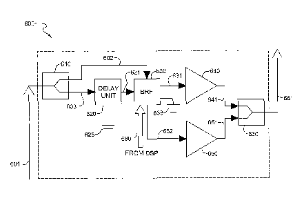
Fig. 6 is a simplified block diagram illustration 600 of a phased shifted
injection
locked push-push oscillator (PSIPPO), in accordance with an exemplary
embodiment of
the invention. In an exemplary embodiment of the present invention the PSIPPO
comprises a power divider 610, a time delay unit 620, a band rejection filter
(BRF) 630,
at least two reflection amplifiers 640 and 650, a power combiner 660.
RECTIFIED SHEET (RULE 91)
CA 02665431 2009-04-02
WO 2008/041222 PCT/IL2006/001144
Fig. 7 is a schematic diagram of the BRF 630 of Fig. 6, according to an
exemplary embodiment of the invention. The BRF 730 comprises at least two
inductors
734, 735 embedded in two isolating transformers able to resonate with the
variable
capacitors 722, 723. Numeral 738 denotes ground. The variable capacitors 722,
723 are
voltage controlled by signals 380 generated by the DSP 390 shown in Figs. 2,
3.
The behavior of the PSIPPO 600 of Fig. 6 will be better understood together
with
Figs. 8A, 8B, 8C, 8D. The PSIPPO 600 receives a signal 601 having a certain
phase and
outputs a signal 661 having the same or a different phase than the input
signal 601.
In an exemplary embodiment of the invention signal 601 is a reference signal
or
1o a signal from a previous PSIPPO and signal 661 is outputted to another
PSIPPO or to a
radiator.
Waveforms 801, 801B in Figs. 8A, 8B are waveform illustrations of input
reference signal 601 for two different voltages V1 and V2 respectively, and
waveforms
861,861B in Figs. 8B, 8D are waveforms illustration of signal 661 for two
different
voltages V 1 and V2, in a particular non-limiting example. The output signal
661 has
twice the frequency and twice the phase angle of the input reference signal
601. A
person skilled in the art will appreciate that the output signal 661 can have
twice the
frequency and about twice the phase angle of the input reference signal 601.
The power divider 610 receives the signal 601 and inject a first portion 602,
illustrated by waveforms 802, 802B in Figs. 8A, 8C and second portion 621
illustrated
by waveforms 821, 821B in Figs. 8A, 8C, into the BRF 630, where the second
portion
621 is obtained by using a time delay unit 620, which creates a time delay of
about half
the period of the reference signal 601. In an alternative exemplary embodiment
of the
present invention, the time delay is predetermined. In an alternative
exemplary
embodiment of the present invention, the time delay is an odd multiple of
about one half
of the period of the reference signal. The signals 602 and 621 entering the
BRF 630
have the same power level, but are opposite in phase. A person skilled in the
art will
appreciate that the signals 602 and 621 entering the BRF 630 may have about
the same
power level.
DECflF6ED SHEET (RULE 91)
11
CA 02665431 2009-04-02
WO 2008/041222 PCT/IL2006/001144
The BRF 630 outputs signals 631, 632 illustrated by waveforms 831, 832
respectively, when the bias voltage of the variable capacitors 622, 623 of BRF
630 has a
value V1. The BRF 630 outputs signals 631, 632 illustrated by waveforms 831B,
832B
respectively, when the bias voltage of the variable capacitors 622, 623 of BRF
630 has a
value V2. In an alternative exemplaiy embodiment of the present invention, the
phase
shift of the output signal relative to the received reference signal is in the
range of about
-100 to about +100 degrees. The reflection ainplifiers 640 and 650 output
signals 641
and 651 correspondingly. Signals 641 and 651' are fed into a combiner 661,
which
outputs signal 661. Signals 641, 651 are represented by waveforms 841, 851
respectively, when the bias voltage of the variable capacitors 622, 623 of BRF
630 has a
value V1. Signals 641, 651 are represented by waveforins 841B, 851B
respectively,
when the bias voltage of the variable capacitors 622, 623 of BRF 630 has a
value V2.
From Figs. 8A, 8B, 8C, 8D it can be noticed that the frequency of the signal
661,
represented by waveforms 861, 861B, has twice the frequency of signal 601.
Furthermore, the phase of waveform 861, corresponding to bias voltage V1,
differs
from the phase of waveform 861B, corre'sponding to bias voltage V2.
Fig. 9 illustrates a PAA, able to steer the antenna beam in azimuth and.
elevation,
in accordance with an exemplary embodiment of the invention. The exemplary PAA
of
Fig. 9 has four elementary blocks 502, 504, 506, 508. Persons skilled in art
will readily
appreciate that the construction of a PAA can be made of a plurality of
distributed
elementary blocks, and that the present exainple is shown for the convenience
of
providing a simple and clear explanation of the present invention. In Fig. 9
numerals
541, 542, 543, 544, 545, 546, 547, 548 refer to radiators, numerals 571, 572,
573, 574,
575, 576, 577, 578 refer to amplifiers, numerals 561, 562, 563, 564, 565, 566,
567, 568
refer to mixers, numerals 551, 552, 553, 554, 555, 556, 557, 558 refer to
sampling
couplers, numerals 512, 514, 516, 518 refer to PSIPPOs used to steer the
antenna beam
in the elevation direction, and numerals 531, 532, 533, 534, 535, 536, 537,
538 refer to
PSIPPOs are used to steer the antenna beam in the azimuth direction. In an
exemplary
embodiment of the invention PSIPPOs 531, 533, 535, 537 are being phase shifted
by
3o angle (31, (33, 05, (37 respectively, PSIPPOs 532, 534, 536, 538 are being
phase shifted
12
CA 02665431 2009-04-02
WO 2008/041222 PCT/IL2006/001144
by angle f32, (34, (36, (38 respectively, and PSIPPOs 512, 514, 516, 518, are
being phased
shifted by angle al, a2, a3, a4 respectively. In a particular example angles
(31 = J33 =
(35 = (37= 100 degrees, angles (32 = (34 = (36 = (i8 = 0 degrees, and angle
al= -150
degrees, angle a2= -50 degrees, angle a3 = +50 degrees, angle a4 =+150
degrees.
Other angles will be readily appreciated from the above exainple.
The system described in Fig. 9 is an example of simple PAA, able to steer the
beam in elevation and azimuth. Taking as reference the block 502, the signal
generated
by the distributed network of PSIPPO has the purpose of providing the mixers
561, 562
with the proper RF pump, for up-converting the modulating signal. The
modulating
signal will enter the mixers as indicated by the arrows shown in the symbols
of the
mixers. The sampling capacitors 551, 552 have the purpose of providing the
down
converters of the receiver (not shown) with the proper pump for down-
converting the
received signal.
Fig. 5 also demonstrates a distributed PAA architecture, in the sense that a
PSSIO, such as 512, 514, 516, 518 affects more than one radiator, while in a
non-
distributed architecture such as demonstrated by Fig. 1 a phase shifter in a
T/R module,
for instance 112, 114, 116 or 118, affects only oneradiator.
Fig. 10 illustrates a wireless networlc system 250, in accordance with
exeinplary
embodiments of the invention. In accordance with the system 250 an enllanced
and
iinproved wireless cominunication network is disclosed. System 250 comprises a
plurality of wireless access point 252, 254 each using a PAAs 256, 258 that
transmit and
receive signals 260, 262, 264, 266, 268. A portion of the signals 260, 262,
264, 266 is
used for cominunication between a plurality of wireless devices such as
personal
computers 270, 272, 274 and hand held device 278. The wireless devices can
access a
first network 280 through the use of access point 252 and can thus
cominunicate with
other remote coinputers 284 or other remote portable devices, which may
include hand
held devices and wireless telecommunication devices, including wireless and
network
phones. In the present exemplary figure the first network 280 and second
network 282
are not connected via a hard line. Access points 252, 254 using the PAAs of
256, 258 of
the present invention are in communication range and can therefore bridge
between the
13
CA 02665431 2009-04-02
WO 2008/041222 PCT/IL2006/001144
first and the second networks 282. The use of wide band access points 256, 258
which
may einploy Wi-Fi or Wi-Max technology can assist in allowing communication
between remote coinputers 284, 286. The use of the wireless access points 252,
254,
having PAAs of the present invention will enable significantly more users to
access and
use each wireless access point as a result of the use of the new and improved
PAAs
shown in accordance with the present invention. The use of PAAs 252, 254
having a
plurality PSIPPOs (not shown) would therefore allow the provision of service
currently
not available, such as network phone usage, video telephone calls, significant
data
download and upload capabilities and any other service which require
additional
1 o bandwidth and the ability to handle many more users or subscribers with a
lower
amount of access points.
Fig. 11 illustrates a satellite mobile television system 200 in accordance
with
exemplary embodiments of the invention. A satellite 202 transmits signals 204.
A PAA
206, placed on a roof or other location visible to the slcy of a vehicle 210,
receives the
signals and transmits corresponding signals to a television set (TV) placed
inside the
vehicle 210. Persons skilled in the art will appreciate that the above systems
are
exemplaty and serve to explain some of the many available applications for the
new and
improved PAA of the present invention. In a PAA, according to exemplary
embodiments of the invention, a plurality of PSIPPO are used and when the
PSIPPO are
organized in certain exemplary architectures of the invention, the resulting
PAA is
advantageous, such as lower cost or lower power consumption. It will be
further
appreciated that the PAA of the present iilvention can be used for any data
receiving and
transmitting device to include satellite antennas, antennas used by data
exchange or
switching devices and the like.
The present invention has been described using non-limiting detailed
descriptions of embodiments thereof that are provided by way of example and
are not
intended to limit the scope of the invention. It should be understood that
features or
steps described with respect to one embodiment may be used with other
embodiments
and that not all embodiments of the invention have all of the features or
steps shown in
3o a particular figure or described with respect to one of the embodiments. It
is noted that
14
CA 02665431 2009-04-02
WO 2008/041222 PCT/IL2006/001144
some of the above described einbodiments may describe the best mode
conteinplated by
the inventors and therefore include structure, acts or details of structures
and acts that
may not be essential to the invention and which are described as examples.
Structure and acts described herein are replaceable by equivalents, which
perform the same function, even if the structure or acts are different, as
known in the
art. Therefore, only the elements and limitations as used in the claims l'unit
the scope of
the invention. Furthermore, the terms "comprise", "include", "have" and their
conjugates
mean, when used in the claims, "including but not limited to".