Note: Descriptions are shown in the official language in which they were submitted.
CA 02665947 2009-04-07
WO 2008/044250 PCT/IT2006/000712
1
Process for manufacturing combined solar panels of
photovoltaic and thermal type and related solar panel
Technical Field
. The present invention generally refers to a process for
manufacturing combined solar panels of photovoltaic and
thermal type capable of converting the solar energy into both
electric and thermal energy with high efficiency. The present
invention further generally refers to a solar panel
manufactured through such a process.
More particularly, the present invention refers to a process
for manufacturing solar panels comprising, in combination, at
least one photovoltaic panel and one heat-exchanging thermal
panel (heat exchanger).
Background Art
There are known solar panels of photovoltaic and thermal
type(combined solar panels) adapted to convert solar energy
into electric and thermal energy.
For example, from the publication US 2004/0025931 in the name
of the Applicant, it is known a combined solar panel adapted
to simultaneously generate both electric and thermal energy.
A'known solar panel includes a panel or heat exchanger
containing a fluid, and a photovoltaic panel comprising a
plurality of photovoltaic cells and a glass sheet.
More particularly a known thermal exchanger includes a plate
made of a heat-conducting material (plate) glued to a first
-
face of the photovoltaic cells (cells), with a second face of
the cells - to be exposed to the solar energy - which is
protected by the glass sheet (sheet) which too is glued to
the cells.
The process for manufacturing the known combined solar panels
provides that, in order to glue the_ sheet and the plate to
the opposite faces of the cells, a thin transparent layer of
ethyl vinyl acetate (Ethyl Vinyl Acetate or EVA) is
interposed between the sheet and the cells and between the
CA 02665947 2009-04-07
WO 2008/044250 PCT/IT2006/000712
2
cells and the plate. The EVA used in the known process
contains additives for delaying its yellowing (which is
caused by the exposure to the ultraviolet rays during the
operating life of the solar panel) and have the purpose to
prevent a direct contact between the cells and the glass or
plate, to eliminate the interstices that would otherwise be
formed because of a not perfectly smooth surface of the
cells, and to electrically insulate the active part of the
photovoltaic panel.
The cells of the photovoltaic pa;nel are generally glued to
the sheet and to the plate through a vacuum curing
(polymerisation) process carried out in an apparatus known as
"laminator", comprising an upper chamber and a lower chamber
horizontally divided by an elastic membrane. The lower
chamber of the laminator contains an electric plate capable
to maintain an inner temperature rather uniform and constant,
with oscillations within 20 C.
A typical laminating cycle begins by placing the sandwich or
module formed by glass, EVA, photovoltaic cells, EVA and
plate, inside the lower chamber, making vacuum in both
chambers and bringing the laminator to a temperature of about
100 C so as to remove air stagnation (bubbles) from the
sandwich.
The vacuum is then removed from *%the upper chamber, so that
the membrane separating the two chambers uniformly compresses
the module thus favouring the adhesion of the EVA to the
cells, to the front glass and the plate, and the laminator is
brought to a temperature of about 150 C that allows the
polymerisation of the EVA. This step can last from 10 to 20
minutes.
Firially the temperature is lowered to 100 C and air is slowly
admitted.
It is stressed that the parameters of the lamination cycle
are always selected as a result of a trade-off among the
CA 02665947 2009-04-07
WO 2008/044250 PCT/IT2006/000712
3 specifications supplied by the EVA manufacturers, the
specific experimentation of the module producers, and an
optimisation of the process times with the aim to increase
the production per hour. In factA on the one hand, in order
to evaluate the lamination quality it is often used the
degree of EVA polymerisation, chemically determined through
its insolubility (by weighing the starting amount of the
polymer and the final dry residue after the thermal
treatment), but on the other hand the finished product has to
be obtained in the shortest time as possible and with a cost
of the electric energy which is optimised in respect of its
quality.
Although the lamination process for manufacturing the
modules is not complex and the lamination discard rate is
pretty low (<2%), the combined solar panels and particularly
the photovoltaic panels are not faultless, even because of
the additional operations that are often manually
accomplished (such as cell alignm4nt, welding of the contacts
between the cells, welding of the termination strings, etc.).
The CEI EN 61215 (CEI 82-8) regulation lists the defects that
can be recognized in a photovoltaic panel through a visual
inspection (test 10.1) and through other inspections, but
does not establish a merit classification which on the other
hand would be useful for an acceptance test of a supply.
A typical defect listed in the above regulation as a defect
that can be recognized through vi:sual..inspection (visually),
it is the breakage of parts of one or more cells, generally
caused by an excessive pressure during the lamination or by
an improper handling of the cells in the assembly step.
Besides the defects that can be visually recognized,
there are defects that cannot be~ visually detected and are
surely more insidious.
CA 02665947 2009-04-07
WO 2008/044250 PCT/IT2006/000712
4
Of course there are methods adapted to verify existence of
defects before installing the solar panel, but since as a
general rule they are time-consuming tests and some times
invasive and requiring expensive equipments, the detection of
these defects is generally committed to the guarantee
supplied by the factory quality control on samples (by using
anyway the reference regulations for the number of the
samples in order that the tests are statistically
meaningful).
Among the most common defects that cannot be visually
detected there are the so-called "hot spot."
The hot spots are locations of the solar panel (panel) at
which, in the operating panels, a temperature is detected
that is higher by some degrees than that of the remainder of
the panel, which temperature excess..is caused by an high
electric resistance, usually caused by defective welding. The
hot spots can be detected; for example, through IR imaging
(infrared analysis) of the panel under working conditions.
Defective welding also causes electric disconnection of panel
portions, possibly after years of regular exposition and
working.
Among the defects that cannot be visually detected, one of
the most common is the EVA yellowing after several years of
operating life. Early optical degradation of the EVA by
altering the colour towards a',characteristic yellow-brown
colour decreases the transmittance value. The main cause of
the yellowing is a low polymerisation degree (<70%) and an
improper stocking of the EVA before the lamination.
Generally this defect doesn't determine appreciable
reductions of the solar panel performance per se.
Rather a more serious drawback arises from the associated
production of acetic acid released by the EVA decomposition
in contact with the cells, that can induce the corrosion of
CA 02665947 2009-04-07
WO 2008/044250 PCT/IT2006/000712
ele-ctrically conductive parts, such as electric contacts,
etc.
Still more serious are the panel delaminations in use because
of the ungluing among the different layers of the panel.
5 Delamination is generally due 6o a poor cleaning in the
assembly step of the panel or to a low degree of EVA
polymerisation (<700). During type tests (i.e. tests on a
panel sample taken from the production line), delamination is
checked through normalised cycles, fo-r example according to
CEI EN 61215, in a thermal chamber.
Resuming, the Applicant discovered that the known
process for manufacturing composite solar panels brings about
a number of problems the solution of which would allow a
reduction of the defectiveness of the panels, both those
visible and those that are not visible.
More particularly, the Applicant discovered that, in the
known manufacturing process, the cell welding process and the
lamination cycle are particularly critical and subjected to
introduce defects in the compositd solar panels.
Disclosure of the Invention
It is an object of the present invention to provide a
process for manufacturing a combined solar panel that is
devoid of the above cited defectiveness problems, both
visible and not visible ones.
An additional objects of the present invention is to provide
a solar panel of the photovoltaic and thermal type having a
high overall efficiency.
In accordance with the present inverition, these objects are
accomplished through a process for manufacturing solar panels
of the photovoltaic and thermal type and through a-high
efficiency solar panel as claimed in the attached claims.
The claims constitute integral part of the technical teaching
hereby disclosed in respect of th~ invention.
CA 02665947 2009-04-07
WO 2008/044250 PCT/IT2006/000712
6
In accordance with a preferred embodiment, the process
according to the present invention for.manufacturing combined
solar panels in which there is provided the presence of a
thermal panel and a photovoltaic panel equipped with
photovoltaic cells and a sheet that is transparent to the
solar energy, provides that the cells of the photovoltaic
panel are fixed to the thermal panel and to the transparent
sheet thanks to a discrete number of glue spots and a resin.
In accordance with a further characteristic of the
present invention, the manufacturing process provides that
the resin is introduced into the panel during its
construction by applying a p.rogressive vacuum to the
vertically positioned panel being manufactured.
In accordance with another characteristic of the present
invention, the cells of the photovoltaic panel have contacts
that are associated to rheophores having an increased cross-
section in comparison to that of the contacts so as to
optimise the electric efficiency of the photovoltaic panel by
reducing the voltage drops.
Brief Description of Drawings
The above and other characteristics of the present
invention will result clear from the following description of
preferred embodiments, given only with exemplary and not
limiting purposes, with the aid of the attached figures, in
which components indicated by a same or similar numerical
reference relate to components h.aving the same or similar
functionality and construction, and in which:
Fig. 1 is a perspective and cross-sectioned view of a
combined solar panel according to the invention;
Fig. 2 and Fig. 3 schematically illustrate a first step of a
process according to the invention;
Fig. 4a and Fig. 4b schematically illustrate a second step of
a process according to the invention;
CA 02665947 2009-04-07
WO 2008/044250 PCT/IT2006/000712
7
Fig. 5a, Fig. 5b and Fig. 6 schematically illustrate a third
step of a process according to the invention.
Best mode for Carrying Out the Invention
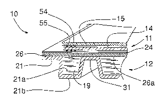
With reference to Fig. 1 a process for manufacturing a
combined solar panel (solar panel) 10 comprising a
photovoltaic panel 11 and a therrri~Ll panel (thermal exchanger)
12 combined together provides, in a first step, the
construction of the thermal exchanger 12.
More particularly, the thermal exchanger 12 is realized as
follows:
- a first sheet (lower sheet) 21 (Fig. 1, Fig. 2) preferably
of a metal, for example stainles's steel, copper, aluminium,
zinc, thermally conducting alloys, etc is press-folded so as
to create on a first face 21 relieves 31 adapted to create,
in known manner, a preferential path for a heat-carrying
fluid (fluid) 19, for example water;
- preferably in correspondence of the path ends, there are
formed respective holes 23 in which pipe sections 23a and
23b respectively (Fig. 1 and Fig. 2) are fitted and welded
for providing an inlet and an outlet to the fluid;
- a second sheet (upper sheet) 26, preferably one flat sheet,
substantially equivalent to the first sheet 21 in respect of
the surface and the material, has a first face or inner face
26a that is welded to the relieves 31- of the first face 21a
of the first sheet 21, so as to form the heat exchanger 12,
i.e. a closed hull adapted to contain the fluid. The so
fozmed heat exchanger (the hull) 12 has a first outer face
26b corresponding to the second face of the second sheet 26,
and a second outer face 21b corresponding to the second face
of the first sheet 21. Preferably the second sheet 26 is
welded to the first sheet 21 in a known manner, by
overlapping and pressing the relieves 31 on the inner face
26a of the second sheet 26. This type of welding, preferably
carried out without filler materi~al and exploiting the known
CA 02665947 2009-04-07
WO 2008/044250 PCT/IT2006/000712
8
Joule effect caused by an electric current passing through
the materials to be welded, is advantageous since it provides
a high sealing level to the pressure of the fluid inside the
heat exchanger 12, when the temperature of the fluid changes;
- preferably, as a complementary step, a layer of a thermally
insulating material of known type 24a, is applied over the
second outer face (lower face) 21b of the hull 12 and a thin
layer or film 24b (Fig. 2, Fig. 3) of an electrically
insulating material, for example mylar or an equivalent
material of known type, is placed in contact with the first
outer face (upper face) 26b of the hull 12. Such
complementary step prepares the heat exchanger to be coupled
with the photovoltaic panel 11 totrealize the solar panel 10.
In a second step there is foreseen to make strings 40
(Fig. 4a, Fig. 4b) of photovoltaic cells (cells) 41 with a
length determined as a function of the panel size (10 - Fig.
1); this second step is a pre-arrangement to the construction
of the photovoltaic panel 11 to be combined with the heat
exchanger 12.
More particularly, the strings 40 (Fig. 4a, Fig. 4b) are
realized as follows:
- a plurality of cells 41, in a number predetermined as a
function of the size of the panel 10, are aligned and welded
together, e.g. in series. The cells 41, of a known type, are
for example cells of crystalline silicon of circular or
octagonal shape, each having on opposite faces, contacts of
opposite polarity, respectively first contacts 42a and second
contacts 42b. In the preferred embodiment, the contacts of
each face, 42a and 42b respectively, are associated to
respective rheophores, first 43a and second rheophores 43b,
so that the first rheophores 43a of a first cell 41 are
connected, for example by welding, to the second rheophores
43b of a second cell 41, and the first rheophores 43a of the
second cell 41 are connected to the second rheophores of a
CA 02665947 2009-04-07
WO 2008/044250 PCT/IT2006/000712
9
third cell 41, and so on. As can be easily understood by the
skilled of the art, such arrangement amounts to a series
connection of the cells 41.
Preferably, the welding is carried out, for example, through
a front/rear welder of a known type..
Still more preferably the cell co.nnecting rheophores, 43a and
-
43b respectively, are made with a larger thickness than
usual. For example the first rheophores 43a are made by
welding to the contacts 42a, generally having a rectangular
cross-section of about 2 x 0,1-0,2 mm, rectangular cross-
section leads of 2,5-3,0 x 0,3 mm, whereas the second
rheophores 43b are made by welding to the contacts 42b a
suitably-sized thin metal sheet preferably comprising one or
more notches or folds 43c, transversally extending with
respect to the welding direction, adapted to prevent the
cell from being subjected to mechanical stress during the
welding.
The so formed rheophores allow to reduce the voltage drop
caused by the connections between a cell and another thus
optimising the photovoltaic panel.efficiency.
-
As a matter of fact, the electric resistance of an electric
connection is given by the known relationship
R =p L/S
where
p = material resistivity
L = conductor length
S = conductor cross-section
Obviously, an increase of the current (power) generated by
the cells brings about an increase of the voltage drop on the
connections (ribbons) between the cells. A way to reduce
CA 02665947 2009-04-07
WO 2008/044250 PCT/IT2006/000712
these voltage drops is to increase- the quantity S i.e. to
increase the thickness of the connections between the cells.
The above described arrangement increases the rheophores's
thickness, thus reducing the voltage drop caused by the
5 electric connections and optimises after all the efficiency
of the photovoltaic panel.
In a third step of the process it is provided that the
photovoltaic panel 11 is directly made and combined with the
heat exchanger 12 (Fig. 1, Fig. 5a, Fig. 5b, Fig. 6), which
10 panel, in accordance with the present embodiment, includes at
least a photosensitive layer 14 comprising one or more
strings 40 of cells 41 and a transparent sheet (sheet) 15,
for example a glass sheet.
The photovoltaic panel 11 are bullt as follows:
- over the film (insulating layer) 24b a number of glue spots
54, for example of silicone with a UV catalyst or
polyurethane are applied according to a predetermined
pattern. In the preferred embodiment, the glue spots 54 are
positioned by means of a numerical control machine or a
robot, and they are arranged in such a way that groups of at
least five glue spots (spots) 54, for-example four peripheral
spots and a central one, correspond to the location at which
each cell 41 of a string 40 has to be positioned. The glue
spots 54 positioned in this way realize a bed of glue spots
or spacers 54 - of an insulating material in the illustrated
example - over which the strings 40 formed in the second
step will rest;
- the spacers 54 are cured or 'catalysed, e.g. by exposing
them to ultraviolet radiations (UV);
- in a known manner the strings 40 are located over the
spacers 54 so as to form the photosensitive layer 14 and are
connected in series to realize (preferably) two series
circuits the opposite polarity ends of which are connected in
a known manner to protection diodes 45. Preferably, the
CA 02665947 2009-04-07
WO 2008/044250 PCT/IT2006/000712
11
diodes 45 are secured to suitably located holes 27 of the
upper sheet 26 of the heat exchanger 12;
- a further number of glue spots 55, for example of silicone
with UV catalyst or polyurethane, are applied over a first
face 15a of the plate 15 at predetermined positions. In the
preferred embodiment the glue spots 55 are positioned by
means of a numerical control mac4ne or a robot, and they are
arranged in such a way that groups of at least five glue
spots (spots) 55, for example four peripheral spots and a
central one, corresponds to the location of each cell 41 of a
string 40. Also in this case the glue spots 55 realize a bed
of- glue spots or spacers 55 adapted to keep the plate 15
spaced from the cells 41;
- the spacers 55 are catalysed, e.g. by exposing them to
ultraviolet radiations (UV);
- the first face 15a of the plate 15 is positioned over the
photosensitive layer 14 so that the spacers 55 rest over the
photosensitive layer 14 and there is no direct contact
between the plate 15 and the photosensitive layer 14;
- the so stacked heat exchanger 12, insulating layer 24b and
photovoltaic panel 11 are seale~ along their sides, along
four sides in the example, so as to form a module or sandwich
18. that is compact and easy to handle. The sealing is
preferably accomplished with polyurethane. In the preferred
embodiment, it is provided that during the sealing on the
sides, a limited zone or area along one side, preferably a
barycentric area, is not sealed and comprises two devices
such as, for example, a sucking pipe 57a and a cannula 57b.
As will be described in more details in the following, these
two devices, 57a and 57b respectively, are adapted to allow
for both the application of a controlled vacuum to the module
18 and the insertion of a filling resin 58 into the zones
between the insulating layer 24b and the photosensitive layer
CA 02665947 2009-04-07
WO 2008/044250 PCT/IT2006/000712
12
- '
14 and between the plate 15 and the photosensitive layer 14
in which the beds of spacers are present;
- the partially sealed module 18 is fixed to a work-table
(not shown) that can be rotated so as to assume an
inclination comprised at least between 0 and 90 ;
- the table is rotated so that the module assumes a
substantially vertical starting position in which the
unsealed limited area 57 is in an upper position;
- through the suction pipe 57a, a given initial vacuum level
is applied to the module 18, for example - 0,1 bar and
through the cannula 57b the highly transparent resin starts
to be introduced into the module 18. According to a preferred
embodiment, the resin 58, e.g. a marketed catalysed resin, is
inserted while at the same time the vacuum is increased
proportionally to the increasing level of the resin in the
module; the cannula 57 is progressively extracted from the
module, leaving however an end bathed by the resin until the
cannula is completely removed at the end of the filling
process. The initial vacuum is advantageous for expelling
possible air bubbles from the module, whereas the vacuum
increase during the introduction of the resin 58
advantageously balance the pressure exerted by the resin on
the module components and prevents possible breakages of such
components;
- once the resin introduction has been completed, the work-
table is rotated so that the module 18 substantially assumes
a horizontal position (final position). According to a
preferred embodiment the vacuum=is progressively decreased
-
during such rotation, for example in a manner proportional to
the angular change, from a maximum value to a minimum value,
such as for example from 0.5 bars to 0.05 bars. At the end of
the rotation the module will show the minimum inclination,,
such as to avoid the resin spillage, and at the same time
CA 02665947 2009-04-07
WO 2008/044250 PCT/IT2006/000712
13
even the pressure applied by the .resin onto the module
components will be minimum;
- the vacuum is completely removed, the suction pipe 57a is
removed and the sealing is completed. At the end of the
sealing, preferably, the module is maintained in a controlled
environment (in respect of temperature, moisture, etc.) for a
given time such as for example one day, to allow a good
cross-linking of the resin. With'this step the manufacturing
of the photovoltaic panel 11 is completed, as well as that of
the solar panel 10 that it is ready to be installed and used.
According to a preferred embodiment, starting from the
surface to be exposed to the solar energy, a solar panel 10
manufactured through the disclosed process comprises:
- a plate 15, for example a plate of glass or of a plastic
material of known type;
- a first bed of spacers 55, adapted to electrically insulate
the plate 15 and to maintain it at a predetermined distance
from the photosensitive layer 14;
- a second bed of spacers 54, adapted to electrically
insulate the photosensitive layer 14 and to maintain it at a
predetermined distance from the insulating layer 24b covering
- the upper face 26b of the heat exchanger 12;
- the resin 58, adapted to embed the photosensitive layer 14
and to electrically insulate it from the plate 15 and from
the heat exchanger 12;
- the insulating layer 24b;
- the heat exchanger 12 comprising the upper sheet 26, the
heat-carrying fluid 19 adapted to transport the collected
solar energy, the lower sheet 21;
- the layer of thermally insulating material 24a.
Preferably the plate 15 has a high mechanical resistance,
high transparency, high thermal transmittance U(W/m2*K),
high planarity, high hardness, is capable to protect the
lower elements from water infiltrations and from chemically
CA 02665947 2009-04-07
WO 2008/044250 PCT/IT2006/000712
14
reacting pollutants, it is selected so as to not pollute the
substrate through migration processes, it is resistant to
atmospheric abrasion and erosion, it is chemically and
geometrically stable at high temperatures. The plate can be
for example a toughened glass plate of known type.
Preferably the spacers 54 and 55 have high resistance to
ageing and light, high resistance to the large temperature
changes, good adhesion to the substrata, elasticity, a wide
range of operating temperatures, good impermeability to
gases, good electric resistance, elevated chemical inertia
towards the photovoltaic cells and with the cell embedding
material, high optical transparency. For example the spacers
are made of silicone.
The photosensitive layer 14 is preferably formed by
elementary photovoltaic cells o-f crystalline silicon, for
example cells with a power of 2.1 W and size of 125 x 125 mm
from SHARP or from ENI-EUROSOLARE companies. Of course the
manufacturing process and the panel can be used for different
kinds of cells, such as for example thin film cells, gallium
arsenide cells, etc.
The resin or the embedding/blocking material of the cells 58
has preferably a high transparency, high binding power, short
curing times and it is not thermosetting, has a high thermal
dispersion, low viscosity, high resistance to ageing and to
light, including the ultraviolet radiation, high resistance
to' the large temperature changes, an extended range of
operating temperatures (-30 C < T-< 150 C) uniformity and
continuity in the distribution ,. of the mechanical
stresses/tensions, high elastici~y, it is chemically inert
and is a good dielectric.
The resin can be for example a commercial resin of the CE9500
type cured with CE9500 cat. or of the CE100-7 A.E. type cured
with CE100-7 A.E. sold by CAFARELLI RESINS company, or a
CA 02665947 2009-04-07
WO 2008/044250 PCT/IT2006/000712
resin of the NT620 type cured with NT620 cat. of the NEW TECH
company.
Of,course, as will be evident to the skilled of the art, the
resin can also be of other types without departing from the
5 scopes of the invention as described and claimed.
Preferably the heat exchanger 12 is a thermal machine in
which power is transferred to a fluid through a solid
surface. The laws governing such power transfer are
irradiation, convection, forced -convection and conduction.
10 The heat exchanger includes sheets, preferably metal sheets,
having a large thermal conductivity k,..a low "fouling factor"
F = (m2*K/W) both on the side where the cooling fluid flows,
and on the outer side of the exchanger (panel/external
environment border), large resistance to chemical
15 oxidation/reduction processes, and is adapted not to
contaminate the cells through ion migration processes, good
weldability, high deformability and resistance to mechanical
stresses.
Preferably the heat carrying fluid -19 has a large cooling
capability, a low kinematic viscosity (m2/s), and is not
polluting.
Preferably the layer of insulating material 24a is adapted to
provide a large thermal insulafsion, very good protection
against water infiltrations and against polluting agents that
are chemically reactive, is resistant to atmospheric abrasion
and erosion, has a stable insulating power and is
geometrically stable in the time. The insulating material is,
for example, polyurethane foam or plastic material.
In accordance with a preferred embodiment of the above
disclosed manufacturing process, the. glue spots, 54 and 55,
are applied onto the insulating layer 24b and the plate 15,
respectively. According to other embodiments the glue spots
can of course be applied, for example by a numerical control
machine, onto opposite faces of the strings 40 of cells 41
CA 02665947 2009-04-07
WO 2008/044250 PCT/IT2006/000712
16
without departing from the scope of the invention as
disclosed and claimed.
According to a preferred embodiment, the manufacturing
process and the panel provide for the presence of the
insulating layer 24b, but of course, as can be easily
understood by the skilled of the art, the presence of this
layer is not compulsory since both the bed of the spacers 54
and the resin 58 are adapted to electrically insulate the
upper face 26b of the heat exchanger 12 from the
photosensitive layer 14.
Since the solar panel manufactured as disclosed does not
require lamination steps, it is not affected by the
drawbacks deriving from such steps. More particularly, the
lack of lamination steps and the provision of steps for
introducing properly selected resins into the module,
ensures a high quality and a lack-of defects in the short and
medium term.
Moreover, the use of connections between the cells using
conductors of increased thickness optimises the efficiency of
the cells.
Several obvious changes are possible to the above
description in respect of size, shapes, materials,
components, circuit elements and connections, as well as in
respect of the circuitry details, of the illustrated
construction and of the manufacturing process without
departing from the invention as defined in the attached
claims.