Note: Descriptions are shown in the official language in which they were submitted.
CA 02666815 2011-07-29
ELECTROTHERMAL INTERFACE MATERIAL ENHANCER
FIELD OF THE INVENTION
This invention pertains to flexible structures having nanostructures attached
to a
surface, and in particular to deformable thermal and electrical interface
materials using
multiwalled carbon nanotubes.
BACKGROUND OF THE INVENTION
Electrical contacts are vital elements in many engineering systems and
applications at the macro, micro, and nano scales. Reliability and
functionality of
electrical contacts can often be a limiting design factor. A major portion of
electrical
contact resistance comes from the lack of ideal mating between surfaces.
Primary
causes of this problem involve the mechanical properties of the surfaces and
surface
roughness. When two surfaces are brought together, the actual contact area may
be
much smaller than the apparent contact area. The contact between two surfaces
can
1
=
CA 02666815 2009-04-17
WO 2008/049015 PCT/US2007/081667
#1198154
actually be thought of as the contact of several discrete points in parallel,
referred to as
solid spots or a-spots. Thus, only the a-spots act as conductive areas and can
be a
small percentage of the total area.
Since their discovery, carbon nanotubes (CNTs) have been studied intensively
throughout many communities in science and engineering. Several researchers
have
reported on the mechanical, electrical, and thermal properties of individual
single-wall
carbon nanotubes (SWNTs). The electrical properties of SWNTs are affected by
the
chirality of the SWNTs to the degree that the SWNTs can exhibit metallic or
semiconducting electrical conductivity. The electrical transport properties of
a single
SWNT are a well studied subject. It has been shown that for ballistic
transport and
perfect contacts, a SWNT has a theoretical resistance of 6.45 KO, which is
half of the
quantum resistance h/2e2. In MWCNTs, each layer within the MWCNT can have
either
a metallic or semi-conducting band structure depending on its diameter and
chirality.
Due to this variation among layers, the net electrical behavior of a MWCNT is
typically
metallic and a wide range of resistance values, e.g., from 478 0 to 29 KO,
have been
reported.
The use of an individual MWCNT may not be low enough to reduce contact
resistance at an interface significantly. However, by using an array of MWCNTs
as an
inter-facial layer, it is expected that numerous individual contact spots and
contact area
enlargement can create current flow paths through each contact, thus reducing
overall
resistance. An additional advantage to using CNTs is that they can tolerate
high current
densities. Therefore a MWCNT layer can be a potential solution to the
reliability and
functionality issues faced at electrical interfaces.
Various embodiments of the present invention present novel and nonobvious
apparatus and methods for improved structural, electrical, and thermal
interfaces.
2
CA 02666815 2012-06-08
According to an aspect of the present invention, there is provided an
apparatus
comprising:
a compliant, readily-deformable metallic foil having first and second opposing
sides, said foil having a thickness less than 0.025 millimeters; and
a plurality of nanotubes having one end grown from a layer of catalytic
material
on the first side of said foil and a free end, said nanotubes being
substantially aligned
perpendicularly to said first side;
wherein thermal resistance from the free end to the second side of said foil
is
less than about 50 mm2 K/VV;wherein the first side of said foil includes a
layer of adhesive material and a layer
of buffer material between said layer of catalytic material and said layer of
adhesive
material;
wherein the buffer material comprises In, Pb, or Sn, or a combination thereof.
According to another aspect of the present invention, there is provided an
apparatus comprising:
a flexible, separable metallic member having first and second opposing sides;
a first plurality of nanoparticles grown from said first side; and
a second plurality of nanoparticles grown from said second side;
wherein said first plurality are grown simultaneously with said second
plurality;
wherein said member is a composite multilayer structure including a central
substrate, a layer of adhesive material on each said opposing side of the
substrate, an
external layer of catalyst on each said opposing side of the member, and a
layer of
buffer material between each said layer of catalyst and the proximate said
layer of
adhesive material;
wherein the buffer material comprises of In, Pb, or Sn, or a combination
thereof.
3
CA 02666815 2012-06-08
BRIEF DESCRIPTION OF THE DRAWINGS
FIG.1A is a schematic diagram of a photoacoustic (PA) test apparatus.
FIG. 1B is a schematic representation of a nanoparticle assembly according to
one embodiment of the present invention.
FIG. 1C is a schematic representation of a nanoparticle assembly according to
another embodiment of the present invention.
FIG. 2 is a comparison of contact resistance between a bare Cu-Cu Interface
and
a Cu-MWCNT-Cu Interface.
FIG. 3 depicts a classification of the Contact Surface.
FIG. 4a is a typical contact configuration of a bare Cu-Cu contact.
FIG. 4b shows a contact resistance reduction by parallel contacts created by
MWCNTs according to one embodiment of the present invention.
FIG. 5 shows SEM images according to one embodiment of the present invention
of a CNT array synthesized on a Si substrate on a silicon substrate. (a) A 30 -
tilted
plane, top view of the vertically oriented and dense CNT array. The array
height is
estimated to be 15 pm. The CNT array has a part across the top of the image
that
helps illustrate the uniformity of growth. (b) An image with higher
magnification showing
individual CNTs. CNT diameters range from 15 - 60 nm.
FIG. 6 shows SEM images according to one embodiment of the present invention
of a CNT array synthesized on a Cu sheet according to one embodiment of the
present
invention. (a) Cross-section view of the vertically oriented and dense CNT
array. The
array height is estimated to be approximately 20 pm; the inset shows the CNT
array
grown on a 1 cm tall Cu bar. (b) An image with higher magnification showing
individual
CNTs. The CNT diameters range from 15 - 60 nm.
3a
CA 02666815 2010-08-13
exposing the third member to electromagnetic radiation;
heating the nanoparticles by said exposing; and
joining the first member to the second member by said heating.
According to a further aspect of the present invention there is provided a
method comprising:
providing a flexible metallic substrate;
placing on the substrate a catalyst for synthesis of carbon nanotubes;
synthesizing with the catalyst a plurality of carbon nanotubes; and
vertically aligning the plurality of nanotubes relative to the substrate
during said
synthesizing.
BRIEF DESCRIPTION OF THE DRAWINGS
FIG.1A is a schematic diagram of a photoacoustic (PA) test apparatus.
FIG. 1B is a schematic representation of a nanoparticle assembly according to
one embodiment of the present invention.
FIG. 1C is a schematic representation of a nanoparticle assembly according to
another embodiment of the present invention.
a Cu-MWCNT-Cu Interface.FIG. 2 is a comparison of contact resistance between a
bare Cu-Cu Interface and
FIG. 3 depicts a classification of the Contact Surface.
FIG. 4a is a typical contact configuration of a bare Cu-Cu contact.
FIG. 4b shows a contact resistance reduction by parallel contacts created by
MWCNTs according to one embodiment of the present invention.
FIG. 5 shows SEM images according to one embodiment of the present invention
of a CNT array synthesized on a Si substrate on a silicon substrate. (a) A 30 -
tilted
plane, top view of the vertically oriented and dense CNT array. The array
height is
3b
CA 02666815 2010-08-13
estimated to be 15 pm. The CNT array has a part across the top of the image
that
helps illustrate the uniformity of growth. (b) An image with higher
magnification showing
individual CNTs. CNT diameters range from 15 - 60 nm.
FIG. 6 shows SEM images according to one embodiment of the present invention
of a CNT array synthesized on a Cu sheet according to one embodiment of the
present
invention. (a) Cross-section view of the vertically oriented and dense CNT
array. The
array height is estimated to be approximately 20 pm; the inset shows the CNT
array
grown on a 1 cm tall Cu bar. (b) An image with higher magnification showing
individual
CNTs. The CNT diameters range from 15 - 60 nm.
3c
CA 02666815 2009-04-17
WO 2008/049015 PCT/US2007/081667
FIG. 7 is a schematic representation of a system for preparing apparatus
according to one embodiment of the present invention.
FIG. 8 is a schematic representation of different analytical models of the
inventive sample assemblies during PA measurement. (a) The CNT array is not
considered a layer in the PA model, but rather as a contributor to the
interface
resistance between the Si wafer and the Ag foil, Rs,_Ag. (b) The CNT array is
considered
a layer in the PA model; therefore, the component resistances, RSi-CNT and
RCNT-Ag, and
the thermal diffusivity of the CNT array can be estimated. (c) The CNT arrays
are not
considered as layers in the PA model, but rather as contributors to the
interface
resistance between the Si wafer and the Cu sheet, Rsi-cu. (d) The CNT arrays
are
considered as layers in the PA model; therefore, the component resistances,
RSi-CNT3
RcNT-CNT, and RCNT-Cu, and the thermal diffusivity of each CNT array can be
estimated.
FIG. 9 show phase shift as a function of modulation frequency for CNT
interfaces
under 0.241 MPa of pressure. (a) Lumped one-sided interface fitting results.
The
mean-square deviation is 0.5 in phase shift. (b) Resolved one-sided interface
fitting
results. The mean-square deviation is 0.5 in phase shift. (c) Lumped two-
sided
interface fitting results. The mean-square deviation is 0.9 in phase shift.
(d) Resolved
two-sided interface fitting results. The mean-square deviation is 0.3 in
phase shift. The
two-sided fitting data is typical of measurements at each pressure.
FIG. 10 shows thermal resistance as a function of pressure for a two-sided CNT
interface (Rsi-cNT-cNT-cu) measured with the PA method and the 1-D reference
bar
method according to one embodiment of the present invention.
FIG. 11 is a schematic representation of an apparatus according to one
embodiment of the present invention.
4
CA 02666815 2009-04-17
WO 2008/049015 PCT/US2007/081667
FIG. 12 is a schematic representation of an apparatus according to another
embodiment of the present invention.
FIG. 13 is a schematic representation of an apparatus and method according to
another embodiment of the present invention.
FIG. 14 is a schematic representation of an apparatus and method according to
another embodiment of the present invention.
FIG. 15 is a schematic representation of an apparatus and method according to
another embodiment of the present invention.
FIG 16 shows CNT arrays synthesized on both sides of a 10 pm thick CU foil
according to another embodiment of the present invention. The density is ¨108
CNT5/mm2. Both CNT arrays are approximately 50 pm in height and the average
CNT
diameter is approximately 20 nm.
FIG. 17 Thermal resistances of bare foil interfaces, Rfoil and CNT/foil
interfaces,
RcNT/f0,1, as a function of contact pressure.
FIG. 18 Thermal circuit for the CNT/foil interface. The local resistances sum
to
give RCNT/foil=
FIG. 19 Thermal resistance between the two free surfaces of the samples. For
the bare foil, the resistance is the same as Rfoil= For the CNT/Foil the
resistance is the
sum of the two free CNT tip interface resistances.
FIG. 20 CNT arrays synthesized on both sides of aluminum foil according to
another embodiment of the present invention. The insert is a higher
magnification SEM
image that illustrates the CNT diameters in the array.
FIG. 21 Resistive network for the aluminum foil /CNT interface.
FIG. 22 is an exploded schematic representation of an apparatus according to
another embodiment of the present invention.
5
CA 02666815 2009-04-17
WO 2008/049015 PCT/US2007/081667
DESCRIPTION OF THE PREFERRED EMBODIMENT
For the purposes of promoting an understanding of the principles of the
invention, reference will now be made to the embodiments illustrated in the
drawings
and specific language will be used to describe the same. It will nevertheless
be
understood that no limitation of the scope of the invention is thereby
intended, such
alterations and further modifications in the illustrated device, and such
further
applications of the principles of the invention as illustrated therein being
contemplated
as would normally occur to one skilled in the art to which the invention
relates.
The present invention pertains to nanoparticles that are deposited on at least
one
side of a flexible, easily deformable substrate. The substrate with attached
nanoparticles can then be placed in contact with the interface of a device.
The easily
deformable substrate permits the substrate and nanoparticles to closely
conform to
irregularities on the surface of the object. By virtue of this intimate
contact of the
nanoparticles with the object, an interface is formed with improved properties
due to the
presence of the nanoparticles and an apparatus prepared according to various
embodiments of the present invention include improvements in one, some, or all
of the
following properties: increased thermal conductance, reduced electrical
resistance,
absorption of electromagnetic radiation, increased efficiency in converting
electromagnetic radiation to heat, and mechanical support. This list of
properties
provided by the nanoparticles is by way of example only, and is not an
exhaustive list.
In one embodiment of the present invention, a plurality of thermally
conductive
nanoparticles are grown or otherwise adhered to a thin, readily deformable
substrate,
such as a flexible sheet of any solid material, including a foil of metal, and
further
including foil of noble metal. The side of the substrate or foil with
nanoparticles is
placed in contact with a heat source, such as a package containing an
integrated circuit.
Because of their small size and the easy deformation of the foil, the
nanoparticles
6
CA 02666815 2009-04-17
WO 2008/049015 PCT/US2007/081667
readily occupy many surface irregularities of the package. Thus, the heat
transmitted
through the wall of the package is more effectively spread into the foil. The
heat
transfer to the foil can be removed by convection or by phase change if a
phase change
material is placed in contact with the nanoparticles, or if another object is
placed in
contact with the foil, through conduction.
In another embodiment of the present invention, nanoparticles are placed on
both sides of a substrate that is plastically deformable with small amounts of
pressure.
In one embodiment, this member is placed inbetween a source of heat and a sink
for
heat, such as between an integrated circuit package and a finned heat
exchanger.
Since the member plastically deforms under light pressure, it readily adapts
to
irregularities on the adjacent surfaces of the integrated circuit package and
finned heat
exchanger. Further, the nanoparticles will fill in some surface voids and
small
irregularities and any adjacent surface. Therefore, heat is more effectively
transferred
out of the heat source and more effectively transferred into the heat sink.
In some embodiments, the nanoparticles are multiwalled carbon nanotubes
(MWCNTs). Although an individual MWCNT has an electrical resistance measured
in
thousands of ohms, by arranging a high density of MWCNTs on surface of the
member,
the overall resistance is greatly reduced, since the MWCNTs act as resistances
in
parallel.
In yet other embodiments of the present invention, the MWCNTs are exposed to
an electromagnetic field that preferentially aligns the MWCNTs during
deposition and
formation. In one embodiment, the MWCNTs are arranged such that the central
axes of
the tubes are substantially perpendicular to the surface to which they are
attached.
However, the present invention is not so limited and contemplates other
directions of
alignment.
7
CA 02666815 2009-04-17
WO 2008/049015 PCT/US2007/081667
In yet another embodiment, a plurality of nanoparticles is deposited on a
thin,
metallic, easily deformable substrate and used as a shield from
electromagnetic
interference (EMI). This member can be placed at the mating interface between
electrical components or housings. As one example, an electrically conductive
metallic
foil having a plurality of vertically aligned MWCNTs on opposing sides is
placed
between a lid of an electronics housing and the base of the electronics
housing. This
foil easily conforms to irregularities in the adjoining surfaces, and both:
(1) enhances
the housing's blockage of external and internal EMI; and (2) reduces the
electrical
resistance between the lid and the base.
In yet another embodiment, the ability of MWCNTs to convert electromagnetic
energy to heat is utilized to provide localized heating of a component
subjected to an
electromagnetic field. As one example, a member populated with MWCNTs can be
placed at an interface where two thermosetting plastic materials come into
contact.
When the assembly of the plastic materials and nanopopulated member is
subjected to
a microwave field, the MWCNTs cause the thermoset joint to heat and fuse into
a
structural joint.
In one embodiment of the invention there is a product to be used to reduce the
thermal (electrical) interface resistance between two connecting devices such
as an
electronic component and a heat sink (another electrical component). The
invention
includes a metal foil with dense carbon nanotube (CNT) arrays directly
synthesized on
the surface of both sides. Under moderate applied pressure, the metal foil
deforms to
the shape of the interface and the CNTs act to produce a plurality of
thermally
(electrically) conductive surface to surface contact spots which in effect
increases the
real contact area in the interface and reduces the resistance of the interface
to heat
conduction and electrical flow. The invention can also be used with existing
commercial,
8
CA 02666815 2012-06-08
wax-based phase change materials (PCM) to enhance the stability of the PCM in
the
interface and to produce increased thermal conduction through the PCM.
Various embodiments of the present invention pertain to an apparatus that can
be inserted, with or with out the addition of a phase change material, between
a
processor chip or an integrated circuit (IC) device and a heat sink to allow
the chips or
IC devices to operate at lower temperatures.
Various embodiments of the present invention pertain to an apparatus that
can be inserted between an electrical device and a connecting electrical
device to
allow electricity to pass between the devices with lowered resistance.
Various embodiments of the present invention produce a thermal and or
electrical interface resistance lower than other removable interface
materials. The
invention does not require CNT synthesis on the devices to be interfaced,
which allows
for scalable production and implementation with existing thermal (electrical)
systems.
When used without the PCM the embodiment of the invention is dry so it will be
stable
in the interface over continued use. When used with the PCM the embodiment of
the
invention acts to hold the PCM in the interface, increasing the stability of
the PCM in the
interface while enhancing thermal conduction through the PCM.
In some embodiments, dense CNT arrays are directly synthesized on both sides
of metal foil to form a material that is dry, highly conductive, and conformal
to an
interface. In yet other embodiments, wax based phase change material is
combined
with the CNT arrays on the foil which enhances the thermal conductivity of the
wax and
discourages the wax from running out of the interface in its liquid phase. The
enhancement of CNT arrays can be added to any existing interface without the
need to
synthesize CNTs on the interfaced devices (which can be destroyed by the
temperatures required for CNT growth and limits scalability).
9
CA 02666815 2009-04-17
WO 2008/049015 PCT/US2007/081667
The use of an N-series prefix for an element number (NXX) refers to an element
that is the same as the non-prefixed element (XX), except as shown and
described.
The use of the suffix prime after an element number (XX') refers to an element
that is
the same as the non-suffixed element (XX) except as shown and described.
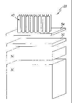
Referring to FIG. 1B, a nanoparticle assembly 20 is shown according to one
embodiment of the present invention and fabricated with three metal layers 50,
52, and
54, including Ti, Al, and Ni, respectively, (thickness: 30 nm, 10 nm, and 6 nm
respectively) deposited on the one side of a copper substrate 30 using
electron-beam
evaporation. Preferably, assembly 20 is adapted and configured to be easily
separable
as an assembly, such that it can be handled as a separate component. Although
various specific quantities (spatial dimensions, materials, temperatures,
times, force,
resistance, etc.), such specific quantities are presented as examples only,
and are not
to be construed as limiting. The Ti layer 50 promotes adhesion of MWCNT 40 to
the
copper substrate 30. The Al layer 52 acts as a "buffer" layer to enhance the
CNT growth
with the Ni catalyst 54 that provides seed sites for CNT growth.
Although various materials are described herein, the present invention also
contemplates usage of other materials. For example, some embodiments of the
present invention utilize a central substrate comprising at least in part
aluminum,
platinum, gold, nickel, iron, tin, lead, silver, titanium, indium, or copper.
Further, yet
other embodiments of the present invention comprise the use of an adhesive
layer
comprising at least in part titanium or chromium. Yet other embodiments of the
present
invention include a buffer material comprising at least in part aluminum,
indium, lead, or
tin. Yet other embodiments of the present invention utilize a catalyst layer
54
comprising cobalt, iron, nickel, or palladium.
The CNTs were grown on this substrate surface by a microwave plasma
enhanced chemical vapor deposition (PECVD) process. The feed gases were H2 and
10
CA 02666815 2011-07-29
CH4. The flow rates of H2 and CH4were 72 and 8 sccm respectively. The H2
plasma
was maintained under a microwave power of 150 W. The process temperature was
800
C, and the growth time was 20 min.
Referring to FIG. 1C, a nanoparticle assembly 20' is shown according to
another
embodiment of the present invention. Assembly 20' includes the nanoparticle
assembly
20 previously described, and includes a mirror image structure on the opposite
side of
central substrate 30. Central substrate 30 further includes an adhesive layer
50' to
promote adhesion of the CNTs to substrate 30. A buffer layer 52' of aluminum
is
deposited on adhesive layer 50'. A catalyst layer 54' is deposited on buffer
layer 52'. A
plurality 40' of carbon nanotubes are grown from catalytic layer 54'.
A schematic of a resistance measurement test setup 10 is shown in FIG. 1A.
Test setup 10 includes a glass plate 12 that supports substrate 30 of a test
sample 20.
Sample 20 is in electrical communication with a multimeter 14. Multimeter 14
is further
in electrical communication with a copper probe 16.1 that is held by an
insulated upper
grip 16.3 of an actuator 16.2. Glass plate 12 is mechanically linked by a
lower grip 18.3
to a load cell 18.1. A CCD camera 19 is positioned to provide data pertaining
to the
interface between the probe 16.1 and the test sample 20.
While subjecting the MWCNT-enhanced Cu substrate 30 to compressive loading
using a Cu probe, electrical resistance change was monitored by a multimeter
14
(Hewlett Packard 3478A). To precisely measure small resistance changes, a
four wire
(point) measurement scheme was adopted. This method eliminates wire connection
resistance and thereby permits pure contact resistance measurement at the
interface.
The probe 16.1 material was also chosen to be Cu in order to match the
properties of
the Cu substrate. The probe tip area is much smaller in dimension than the
substrate so
that multiple
11
CA 02666815 2011-07-29
=
measurements can be made with each specimen by changing the probing
location. To make the probe, the end of a copper nail was polished flat using
a polisher
(Buheler ECOMET VO) and A1203 powder (size: 9 to 1 pm). The polished copper
probe
tip was observed by optical microscope 19 (Olympus BX600), and the image was
digitized using software (Golden Software Didger 2.010) to measure the
apparent
surface area of the probe tip to be 0.31 mm2.
A small-scale mechanical testing machine (Bose Endura ELF 3200 ) was used
to control the probe displacement and to measure the interaction force between
the
probe
11-2
CA 02666815 2011-07-29
and MWCNT-enhanced Cu substrate surface. The position of the probe tip was
adjusted toward the sample surface while monitoring the position of the probe
tip
through a CCD camera. Starting from this non-contacting position (infinite
electrical
resistance) the probe was displaced downward slowly in 1.0 pm increments until
first
measurable electrical resistance was observed. This location was set to be the
initial
position (Z = 0 pm) of the probe, and the probe tip was subsequently moved
downward
by 1.0 pm increments. At each step of displacement, contact resistance and
force data
were recorded. When the resistance displayed a trend close to a constant
value, the
probe descent was stopped. The probe was then moved upward (reverse direction)
in
1.0 pm increments while measuring the contact resistance and force until
electrical
contact was lost (infinite resistance).
The measurements were conducted at two different locations on the same
specimen surface, referred to as Test 1 and Test 2. The resistance ranged from
a
maximum value of 108 0 to a minimum value of 4 0. As the probe was lowered,
resistance decreased.
In Test 1, the position corresponding to the first finite resistance value is
identified as initial electrical contact position (Z = 0 pm). The resistance
did not change
significantly until the probe moved downward past Z = 7 pm. At Z = 11 pm, the
first
measurable reaction force was observed. The electrical resistance then reduced
significantly to a steady value of 4 0 with increased probe movement. Note
that
between the initial position (Z = 0 pm) and Z = 11 pm, there was no measurable
force
but electrical contact was maintained (finite resistance was measured).
In Test 2, the distance between the initial position (Z = 0 pm) and the first
measurable force position (Z = 18 pm) is longer than that of Test 1. This can
be
attributed to the resolution limits of the load cell and contact
characteristics between the
probe and MWCNT layer. In the beginning of contact, a relatively smaller
number of
12
CA 02666815 2011-07-29
=
MWCNT touch the probe tip and thus the force is in the range below the 0.001 N
resolution of the load cell.
Resistance measured while the probe moved upward (reverse process) for the
first several steps (from Z = 20 pm to Z = 14 pm for Test 1 and from Z = 28 pm
to Z = 24
pm for Test 2) showed similar or slightly higher values at corresponding
positions of the
downward measurement. However, the resistance did not increase to an infinite
value
when the probe passed the position from where contact force between two
surfaces
dropped to zero (Z = 13 pm for Test 1 and Z = 23 pm for Test 2). Electrical
contact is
maintained even past the initial position (Z = 0 pm), up to Z = -7 pm for Test
1 and to Z
= -1 pm for Test 2. This trend is opposite to that observed for the bare Cu-Cu
contact.
Also, step-like features of resistance change are evident during both downward
and
upward movements of the probe. These features are thought to be the result of
van der
Waals forces.
The overall trend of force change is more linear than the control case. The
average stiffness during downward movement (0.173x10⁶ N/m for Test 1 and
0.123x10⁶
N/m for Test 2) is approximately two times higher than the initial stiffness
of the bare
Cu-Cu contact (0.067x10⁶ N/m).
The differences in the measured resistance and force between Test 1 and Test 2
are attributed to the global-scale variations of the MWCNT layer. The density
and
morphology of the MWCNT layer generally vary at different probing locations.
Also the
sensitivity of the electrical resistance measurements affects how one defines
the initial
electrical contact position. However, it is notable that after the probe
registers a
measurable force, the trends of contact resistance versus force for both tests
are found
to closely overlap each other, as shown in FIG. 2.
From the previous results, it is clear that the MWCNT layer played a key role
reducing electrical resistance and increasing stiffness. A comparison of the
bare Cu-Cu
13
CA 02666815 2011-07-29
contact and the Cu-MWCNT-Cu contact is shown in FIG. 2. For the same apparent
contact area the Cu-MWCNT-Cu interface showed a minimum resistance of 4 fl
while
the Cu-Cu interface showed a minimum resistance of 20 0. An 80% reduction in
resistance was observed under small compressive loading when MWCNTs are used
as
an interfacial material between Cu surfaces. The average stiffness of the Cu-
MWCNT-
Cu contact is approximately two times larger than that of the bare Cu-Cu
contact.
The mechanism of contact resistance reduction due to the presence of the
MWCNT layer 40 can be explained by two phenomena: (i) enlargement of real
contact
area through numerous parallel contacts, (ii) electrical junctions between
CNTs
combined with compressive loading. Although CNTs can carry large current
densities, it
is known that by simply placing a single CNT on a metal electrode, the contact
resistance was observed to be in the 103 0 to 106 0 range. Also the minimum
resistance between a single CNT and a metal contact can be on the order of 103
0.
However macroscopic contact resistance can be reduced by using a MWCNT layer
containing numerous individual MWCNTs that create parallel paths. Note that
only a
portion of the apparent contact surface which is indicated as A, (a-spots) in
FIG. 3
participates in electrical conduction. In the case of the Cu-MWCNT-Cu contact,
CNTs
significantly increase the size of Ac (a-spots). While this contact situation
is very
complicated, it can be simplified conceptually. As depicted in FIG. 4, the gap
between
two contacting members (see FIG. 4a) is filled with MWCNTs thereby increasing
the
contact area (see FIG. 4b) via numerous parallel electrical contact paths.
FIGS. 4a and
4b show a schematic representation of the tip of copper probe 16.1. FIG. 4b
shows the
probe in contact with a sample 20. FIG. 4a shows a projected contact area
16.4'
between a flat surface and the tip of probe 16.1. FIG. 4b shows the generally
larger
contact area 16.4 present between the tip of probe 16.1 and a nanoparticle
assembly 20
according to one embodiment of the present invention.
14
CA 02666815 2011-07-29
Resistance reduction is also possible though electrical junctions made between
CNTs. The MWCNTs on the substrate's surface exhibit a random configuration
with no
preferential direction. These create electrical junctions among adjacent CNTs
to reduce
the contact resistance. Other researchers suggest that contact resistance vary
widely
depending upon the relative orientation of two CNT surfaces and the level of
1 4-2
CA 02666815 2011-07-29
compressive loading on the junction. When two contacting CNTs are in the A-A
configuration it is called "in registry" which exhibits lower contact
resistance than the A-
B configuration ("out of registry"). For example, in the case of an "in
registry" junction,
the resistance is 2.05 MD for rigid tubes. If compressive force is applied on
this junction,
the resistance is reduced to 121 KO. In real cases, the junction resistance
likely falls
between the lower and the higher resistances. Therefore it is believed that
the
ensemble of the numerous contacts and junctions created during the probe
movement
dictate the macroscopic contact resistance.
For the Cu-MWCNT-Cu interface, the force increased almost linearly when the
Cu probe moved downward. However for the bare Cu-Cu contact, the force did not
increase in a steady manner and was less than that of the Cu-MWCNT-Cu contact.
Note that if the load bearing area is increased, then the force will increase
accordingly.
Thus it can be concluded that MWCNT layer is also effective in enlarging the
load
bearing area.In yet another embodiment of the present invention, CNT array
samples were
grown on Si (Ra = 0.01 pm and Rz = 0.09 pm, calculated by ASME B46.1-2002) and
Cu
(Ra = 0.05 pm and Rz = 0.5 pm, calculated by ASME B46.1-2002) surfaces with a
tri-
layer (Ti/Al/Ni) catalyst configuration by direct synthesis with microwave
plasma-
enhanced chemical vapor deposition (PECVD) employing H2 and CH4 feed gasses.
Si
and Cu were chosen as growth substrates in order to assemble an interface that
is
representative of a common heat sink-processor chip interface. Similar to the
work of
Xu and Fisher, the thicknesses of Ti, Al, and Ni metal layers were 30 nm, 10
nm, and 6
nm respectively. The working pressure of the PECVD chamber was 10 tone, the
sample
stage temperature was 800 C, and the microwave plasma power was 150 W. The
volumetric flow rates of H2 and CH4 were 72 sccm and 8 sccm respectively, and
the
growth period was approximately 20 minutes.
15
CA 02666815 2011-07-29
FIG. 5a shows a 30 -tilted plane, top view of the CNT array synthesized on Si.
The array height is approximately 15 pm. CNT diameters for the array on the Si
wafer
range from 15 - 60 nm (FIG. 5b). FIG. 6 shows that, with identical catalyst
preparation,
the CNT array synthesized on a Cu sheet is very similar to the array on the Si
wafer.
The array height is approximately 20 pm (FIG. 6a), and the CNT diameters also
range
from 15 - 60 nm (FIG. 6b).
A CNT array was grown on a Cu block, which protruded into the plasma and had
sharp edges, in a prior study (inset of FIG. 6a). The block acted like an
antenna to
concentrate the plasma energy around its corners and edges. This plasma
concentration had a strong etching effect on the CNT growth surface. By
comparison,
the height and density of the array on the Cu sheet is greatly improved
because the
plasma did not concentrate on the sheet during CNT growth.
The CNT density, determined by counting CNTs in a representative area of a
scanning electron microscope (SEM) image, was approximately 6x10⁸ CNT/mm2.
Assuming an average CNT diameter of approximately 30 nm, an approximate CNT
volume fraction of 42% can be calculated by assuming the CNTs are circular
tubes of
uniform height that are packed in vertical alignment. Some embodiments of the
present
invention contemplate volume fractions of about 30 percent to 50 percent.
Considering
the lower porosities in comparison with fullerenes, multi-walled CNTs should
possess a
mass density between that of fullerenes, 1900 kg/m3 and graphite, 2210 kg/m3.
Thus,
by assuming a multi-walled CNT mass density of approximately 2060 kg/m3, the
effective mass density of all the CNT arrays (including effects of void space)
in this work
is estimated to be approximately 865 kg/m3.
For some of the test specimens prepared according to one embodiment of the
present invention, a photoacoustic technique was used to measure resistance.
In
photoacoustic (PA) measurements a heating source, normally a laser beam, is
16
CA 02666815 2011-07-29
periodically irradiated on a sample surface. The acoustic response of the gas
above the
sample is measured and related to the thermal properties of the sample. The PA
phenomenon was first explained by Rosencwaig and Gersho, and an analytic
solution
of the PA response of a single layer on a substrate was developed. A more
general
analytic solution derived by Hu et al. that explains the PA effect in
multilayered materials
is used in this study. A review of the PA technique was given by Tam, and the
technique has been used successfully to obtain the thermal conductivity of
thin films.
The PA technique has also been used to measure the resistance of atomically
bonded
interfaces, for which resistances were orders of magnitude less than the
resistances
measured in this study. The use of the PA technique for the measurement of
thermal
resistance of separable (non-bonded) interfaces has not been found in the
literature.
Also, the use of the PA technique with a pressurized acoustic chamber and
sample has
not been found in the literature.
A schematic of the experimental setup 1 is shown in FIG. 7. A fiber laser 3.1
operating at a wavelength of 1.1 pm is used as the heating source. Laser power
is
sinusoidally modulated by an acoustic-optical modulator 3.2 driven by a
function
generator 3.3. For this study, the modulation frequency ranges from 300 - 750
Hz. The
output power of the laser is approximately 350 mW in the modulation mode.
After being
reflected and focused, the laser beam is directed onto the sample 20 mounted
at the
bottom of the sapphire PA cell 2.1. The PA cell is pressurized by flowing
compressed
He 2.2 as shown in FIG. 7, thus providing a uniform average pressure on the
sample
surface. The PA cell pressure is adjusted using a flow controller and is
measured by a
gauge attached to the flow line. The test pressures are chosen to span a range
of
pressures commonly applied to promote contact between a heat sink and a
processor
chip. A microphone 4.1, which is built into the PA cell, senses the acoustic
signal and
transfers it to a lock-in amplifier 4.2, where the amplitude and phase of the
acoustic
17
CA 02666815 2011-07-29
signal are measured. Element 4.3 personal
17-2
CA 02666815 2011-07-29
computer, which is connected to the GPIB interface of the lock-in amplifier
and function
generator, is used for data acquisition and control of the experiment.
For the one-sided CNT interface prepared according to one embodiment of the
present invention, Ag foil (Ra = 0.06 pm and Rz = 0.4 pm, calculated by ASME
B46.1-
2002) forms the top of the sample, while for the two-sided CNT interface
according to
another embodiment of the present invention the side of the Cu sheet not
coated by the
CNT array is the effective top of the sample. The sample structures according
to
various embodiments of the present invention are shown schematically in FIG.
8. To
prepare the samples for PA measurements, an 80 nm top layer of Ti was
deposited by
electron beam deposition, thus allowing for the Ti film to absorb the same
amount of
laser energy as the Ti film on the reference sample during measurements. The
Ag foil
(hard, Premion0 99.998% (metals basis); Alfa Aesar, Inc.) was 25 pm thick, and
the Cu
sheet (Puratronic0 99.9999% (metals basis); Alfa Aesar, Inc.) was 50 pm thick
to allow
for high sensitivity to the total interface resistance of the one-sided and
two-sided CNT
interfaces, respectively. The Si wafers (double-side polished and < 1 0 0 >
orientation;
Universitywafer.com) were 565 pm thick to ensure that the layer is thermally
thick.
Although particular thicknesses of silver and copper foil for the substrate
have been
shown and described, the present invention is not so limited, and contemplates
the use
of foil as thick as about 0.1 millimeters. Further, although various purities
of silver and
copper have been described, the present invention is not so constrained and
contemplates the use of foils with significantly more impurities that are
cheaper and
more commercially available.
The one-sided CNT interface sample has an upper and lower measurement limit
of - 100 mm2-KNV and - 0.1 mm21KNV, respectively. The two-sided CNT interface
sample has an upper and lower measurement limit of - 35 mm2-KNV and - 0.4
mm2-KM/ respectively. The use of the hard, 25 pm-thick Ag foil in the one-
sided CNT
18
CA 02666815 2011-07-29
.h,
sample instead of the 50 pin-thick Cu sheet allows for greater measurement
sensitivity
to the expected interface resistance values. Cu sheets less than 50 pm thick
can
improve measurement sensitivity as well; however, reduction in interface
resistance
resulting from the sheet's surface conformability (deformation between
asperities) are to
be carefully considered in such a case.
In general, the range of measurable resistances expands as the ratio of the
thermal penetration depth to thickness increases for the top substrate (Ag and
Cu in this
work). The upper measurement limit results when the sample's effective thermal
penetration depth is insufficient for allowing heat to pass through the
interface and into
the Si substrate; in this limit the interface is thermally thick. The lower
measurement
limit results when the sample's effective thermal penetration depth is much
larger than
the 'resistive thickness' of the interface; in this limit the interface is
thermally thin. For
the frequency range and sample configurations of this study a 1-D heat
diffusion
analysis is applicable because the largest in-plane thermal diffusion length
in the
layered one-sided CNT sample, I / = 0.43 mm, and two-sided CNT sample, I /ac,,
=
0.35 mm, are much less than the laser beam size (approximately 1 mm x 2 mm).
A reference or calibration sample is used for PA measurements in order to
characterize signal delay due to the time needed for the acoustic wave to
travel from the
sample surface to the microphone and acoustic resonance in the cell (resonance
was
not experienced for the cell in the frequency range of this study). A 565 pm-
thick Si
wafer with a top 80 nm layer of Ti, deposited by electron beam deposition, was
used as
the reference sample (for uniformity, Ti was deposited on the reference and
test
samples at the same time).
The reference was tested with the PA cell pressurized at different levels,
including the pressure levels at which the samples were tested. According to
PA
19
CA 02666815 2011-07-29
theory, phase shift is independent of cell pressure, while amplitude is
proportional to cell
pressure. However, the signal delay may be pressure-dependent for both phase
shift
and amplitude. The composition of the cell gas can change the nature of the
cell signal
delay as well. Air, N2, and He were observed to cause different signal delay
responses.
Of these gases, He produced the highest signal to noise ratio, which is
expected
because the thermal conductivity of He is approximately an order of magnitude
higher
than that of air or N2. He was therefore used as the cell gas for this work.
The thermal
diffusion length in the He filled PA cell, 1/ aHe = 0.46 mm (at atmospheric
pressure), is
much less than the PA cell radius (4 mm) which supports the assumptions of the
PA
model.
Using the PA technique, the thermal resistance of a one-sided CNT interface
(Si-
CNT-Ag) has been measured at 0.241 MPa, and the thermal resistance of a two-
sided
CNT interface (Si-CNT-CNT-Cu) has been measured as a function of pressure. The
PA
technique has also been used to measure the component resistances of the CNT
interfaces and the thermal diffusivities of the CNT arrays. All CNT interface
measurements were performed at room temperature. After testing, the interfaces
were
separated, and the CNT coverage on the Cu and Si substrates was observed
visually to
match the pre-test condition. This resiliency is the result of the strong
anchoring of the
arrays to their substrates enabled by the tri-layer catalyst.
FIG. 9 illustrates the fitted phase shift results at 0.241 MPa for the CNT
interface
samples. FIGS. 9a, 9b, 9c, and 9d, correspond to FIGS. 8a, 8b, 8c, and 8d,
respectively. To establish a benchmark for the accuracy of the PA technique, a
commercial PCM (Shin-Etsu 25 x 25 mm thermal pad; Shin-Etsu Chemical Co.,
Ltd.)
interface (Si-PCM-Cu) was tested. The PCM changes phase at 48 C and has a
reported resistance of 22 mm2-KNV for a 50 pm-thick layer. A resistance of 20
mm2.KNV
was measured with the PA technique for an approximate interface temperature of
55 C
20
CA 02666815 2011-07-29
=
and pressure of 0.138 MPa, which is in good agreement with the manufacturer's
published value.
One-sided CNT interface results are shown in Table 1, and two-sided CNT
interface results are illustrated in FIG. 10 and displayed in detail in Table
2. The
resistances at CNT-substrate interfaces (and CNT-CNT interface for the two-
sided
interface) and the intrinsic conductive resistance of the CNT arrays are
grouped into the
measured total interface resistances, Rsi_Ag and Rsi-cu- This lumping approach
has no
effect on the measured results because during each measurement the laser
energy
penetrates deep enough to completely pass through Rsi_Ag and Rsi-cu and into
the Si
substrate.
Table 1. One-sided CNT interface results.
Rsi-asiT (rnal2 K/W) Fitted parameters
2.3 0.4 Measured values at 241 kPa
RcNT-Ag (mm2 K/W)
13.4 0.2
**R-rotai (Rsi_Ag)(mm2 KNV)
'15.8 0.2
acNT S-on-Si(M2/S)
1.7 0.3 x 10⁴
Table 2. Two-sided CNT interface results.
Rsi-CNT (mm2 KNV) Fitted parameters
Measured values at 172
kPa 0.8 0.5
Measured values at 241
kPa 0.8 0.5
RcNT-CNT (mm2 K/W)
2.1 0.4
2.1 0.4
RcNT-Cu (MM2 KAN)
1.0 0.5
0.9 0.5
**R-rotal (Rsi_Ag) (mm2 KNV)
4.1 0.4
4.0 0.4
acNT S-on-Si(M2/S)
3.2 0.4 x 10⁴
2.3 0.4 x 10⁴
acNT S-on-CA12/S)
2.1 0.4 x 10⁻⁴
4.3 0.5 x 10⁻⁴
21
CA 02666815 2011-07-29
**Obtained from data fit where CNT arrays are not considered as a layer in the
PA
model.
At a pressure of 0.241 MPa the one-sided CNT interface produces a thermal
resistance of approximately 16 mm2.K/W. This photoacoustically measured
resistance
compares well with one-sided CNT interface results obtained using a steady
state, 1-D
reference bar measurement technique. The resistances at the CNT-substrate
interfaces, R5i-CNT and RCNTAg, are approximately 2 mm2.KM/ and 13 mm2.KM/
respectively, and it is clear that the CNT array free tips to substrate (RCNT-
Ag) interface
dominates the thermal resistance of the one-sided CNT interface. A similar
characteristic for one-sided CNT interfaces was reported in a previous study
as well. A
thermal diffusivity of approximately 1.7 x 10⁻⁴ m2is is measured for the CNT
array on the
Si wafer in the one-sided CNT interface sample.
At moderate pressures, 0.172 - 0.379 MPa, the two-sided CNT interface
produces stable and low resistances near 4 mm24K/W. For comparison, resistance
values of a two-sided CNT interface measured with a reference bar method are
also
included in FIG. 10. FIG. 10 demonstrates that the PA results are similar to
the
reference bar results and fall well within the latter results' uncertainty
range. The
pressure dependent, two-sided CNT interface results validate a prior postulate
that data
scatter in the resistance¨pressure characteristics of the reference bar
measurements is
due to the large uncertainty associated with the method. The resolved
resistances of
the two-sided CNT interface, R5i-CNT, RCNT-CNTI and RCNT-Cu, are approximately
1
mm2.K/W, 2 mm2-KNV, and 1 mm2-K/W respectively, and the CNT-CNT interface
dominates the thermal resistance of the interface. The CNT arrays in the two-
sided
interface have measured thermal diffusivities ranging from approximately 2.1 -
4.3 x 10⁻⁴
m2/s.
22
CA 02666815 2011-07-29
With the thermal diffusivities measured in this study ranging from
approximately
1.7 - 4.3 x 10⁻⁴ m2/s and assuming the CNT arrays' room temperature effective
specific
heat to be approximately 600 J/kg=K, the effective thermal conductivities
(including
effects of void space) of the CNT arrays in this study are calculated to range
from
approximately 88 - 223 W/m-K. This estimated thermal conductivity range is
higher than
the thermal conductivity range, 74 - 83 W/m-K, reported for CNT arrays
measured using
the 36) method. Yang et al. reported CNT array thermal conductivities
averaging 15
W/m.K.
The thermal performance revealed by the PA measurement of the one-sided CNT
interface can be attributed to the increase in real contact area enabled by
the high
density of CNT to surface contact spots. The thermal performance revealed by
the PA
measurements of the two-sided CNT interface can be attributed to an even
larger
increase in real contact area. The contact area between the two arrays is
maximized
during the initial loading procedure, so that further increases in pressure do
not cause a
significant increase in array-to-array CNT penetration. Compared to the
resistances of
a bare Si-Cu interface and a one-sided CNT interface (Si-CNT-Cu), which range
from
105- 196 mm2-KNV and 20- 31 mm21KNV respectively, a two-sided CNT interface
produces much lower thermal contact resistance.
An interface with a CNT array directly synthesized on one side of the
interface
has been measured to have a resistance less than 25 mm2KNV, which is equal to
the
resistance of the state of the art commercial thermal interface materials. An
interface
created with a directly synthesized CNT array on one side of the interface and
a wax-
based phase change material (PCM) added to it has been measured to have
resistances below 5 mm2KNV. An interface with a CNT array directly synthesized
on
both sides of the interface has been measured to have a resistance of 4
mm2KIW,
which is similar to the resistance of a soldered joint. However, in
applications where
23
CA 02666815 2011-07-29
the materials that form the interface can not be exposed to the temperatures
normally
used for CNT growth, direct synthesis of CNT array interfaces is difficult to
implement.
In addition, when interface surfaces are relatively rough (e.g. unpolished Cu-
Cu
interface as apposed to Si-glass interface) it can be difficult to directly
synthesize CNT
arrays dense and long enough to adequately fill the interface voids. Some
embodiments of the present invention include a new CNT thermal interface
material
(TIM) with CNT arrays directly synthesized on both sides of a metal foil. The
invention
eliminates the need for exposing temperature sensitive materials and devices
to normal
CNT growth conditions (¨ 900 C) and provides greater conformability to rough
interfaces due to the metal foils ability to match to the interface geometry.
Some embodiments of the present invention can be inserted into several
different interface configurations; however, it differs from other TIMs in
that it is dry,
removable, and has an intrinsically high thermal conductivity. The thermal
interface
resistance of the invention (without PCM) is measured using a photoacoustic
technique.
A resistance of 7 mm2KNV was measured for a Cu-invention-Cu interface under
moderate pressure.
Many parameters affect the performance of metal foils as thermal interface
materials. Qualitatively, the thermal resistance of a metal foil interface
depends on the
thermal and physical properties of the contacting members, foil, and gas gap,
the
contact geometry, the contact pressure, and the interface temperature. While
the
foregoing functional dependencies are difficult to resolve analytically,
empirical
correlations have been developed that match experimental results reasonably
well.
Experimental observations have revealed the existence of a range of preferred
thicknesses, for which thermal resistance is a minimum independent of contact
pressure, for metal foils used in a given interface. Additionally, the
parameter kfoll/Hfoii
where kfoil and Hfoil are the thermal conductivity and the hardness of the
metal foil,
24
CA 02666815 2011-07-29
respectively, has been suggested as a good measure to predict the performance
of a
metal foil in a given application. Higher kfoilififoii ratios reduce thermal
resistance at the
interface.
For metal foils with CNT-enhanced surfaces, heat flow paths and resulting
thermal models become substantially more complicated. In addition to the
properties of
the metal foil, the effective thermal and physical properties of CNT/foils
depend on,
among other factors, CNT density, CNT diameters in the array, and the bonding
of the
CNTs to the foil. Previous studies have shown not only that CNT arrays conform
well in
an interface but also that they have relatively high effective thermal
conductivities (-80
W / m K) and can be bonded well to their growth substrate. These CNT array
properties
can be exploited, through optimization, to create a CNT/foil material whose
effective
thermal to effective hardness ratio kcwrifoii I HCNT/foil is greatly increased
as compared to
a bare metal foil. Both km-moil and Ficgrifoil are affected by the CNT array
properties;
however, reducing Hcro-ifon is expected to be the primary means to increase
kCNT/foil
HCNT/foil Also, CNT/foil characteristics such as the thicknesses of the CNT
arrays and
the metal foil can be controlled such that the contact geometry allows
interfacial void
spaces to be filled completely, thus overcoming the resistance to heat flow
caused by
the roughness of a given interface.
Plasma-enhanced chemical vapor deposition (PECVD) was used to synthesize
the CNT arrays 540 according to some embodiments of the present invention.
Referring
to FIGS. 16 and 17, a trilayer catalyst configuration 550, 552, 554 (30 nm Ti
/ 10 nm Al /
3 nm Fe, respectively) was deposited on both sides of 10 pm thick Cu foil
substrate 530,
according to another embodiment of the present invention. The PECVD process
gases
were H2 [50 SCCM (SCCM denotes cubic centimeter per minute at SIP)] and CH4
(10
SCCM), and the growth pressure and temperature were 10 Torr and 900 C,
respectively. A 200 W plasma was formed in the growth chamber, and CNT
synthesis
25
CA 02666815 2011-07-29
=
was carried out for 10 min. Figure 16 contains a scanning electron microscope
(SEM)
image that shows a side view of the two CNT arrays synthesized on the Cu foil.
As
determined from microscopy (SEM and transition electron microscope) and Raman
spectroscopy, the structural characteristics (e.g., prevalence of CNT defects
and
amorphous C) of the CNT arrays are similar to CNT arrays grown on Si in
previous
work. Each array 540 is fairly uniform in height (approximately 50 pm) and the
average
CNT diameter is approximately 20 nm. The density of each array is preferably
greater
than greater than ¨ 107 CNT/mm2 and preferably is ¨ 108 CNTs/mm2.
The room-temperature thermal interface resistance of a CNT/foil TIM and bare
10 pm thick Cu foil was measured as a function of pressure using a
photoacoustic (PA)
technique, The pressure range was chosen to identify the effects of CNT
enhancement
in a range applicable to the thermal management of electronic components. Two
different interfaces, in which the CNT/foil and bare foil were inserted, were
assembled to
identify the effects of surface roughness on the performance of the CNT/foil
TIM. To
enable the most accurate PA measurements, both interfaces use Ag for the top
substrate in the interface. The Ag is relatively smooth, having an average
surface
roughness Ra of 0.06 pm and an average peak-to-valley surface height Rz of 0.4
pm. A
polished Si base, having Ra=0.0I pm and R=0.09 pm, was used as the opposing
substrate in the first interface (Si-Ag). A Cu base, having Ra=2.8 pm and
Rz=9.3 pm,
was used as the opposing substrate in the second interface (Cu-Ag). The total
thermal
resistances of the CNT/foil, RcNTifoii, and of the bare foil, Rhyd, for the
two different
interface configurations are presented in Fig, 17.
For both configurations, the CNT/foil was examined before and after testing to
assess any permanent physical changes to the material. For the Si-Ag
interface, the
assembly 520 of CNT/foil had an appearance that closely resembled the pretest
condi-
tion upon removal. For the rough Cu-Ag interface, deformation of the CNT/foil
assembly
26
CA 02666815 2011-07-29
520 was apparent such that its shape matched the interface geometry. In each
case,
upon separation of the interface, the CNT arrays 540 remained fully intact on
the
surfaces of the foil. To illustrate its robustness, after removal, the
CNT/foil was retested
in each interface, and the measured thermal resistances were consistent with
the initial
tests.
The bare Cu foil and the CNT/foil TIMs produce very low thermal resistances in
both interface configurations. This result is expected because of the
relatively smooth
contacting member surfaces, The plots of Fig. 17 illustrate that the CNT
arrays provide
greater enhancement to the thermal conductance of the Cu foil in the rougher
Cu-Ag
interface. A reduction in resistance of approximately 30% is achieved at a
contact
pressure of 275 kPa. For the smooth Si-Ag interface, enhancement results when
sufficient contact pressure is applied, and an approximately 15% reduction in
resistance
is achieved at a contact pressure of 275 kPa. Various embodiments of the
present
invention contemplate the use of contact pressures greater than about 50 kPa.
The CNT/foil assembly 520 increases conduction in the interface by two
mechanisms, both of which cause an increase in the number density of contact
points
between free CNT tips and their opposing substrate. The first mechanism is the
deformation of the CNT arrays 540 and the second is the deformation of the
foil
substrate 530. We postulate that the CNT array deformation is elastic (i.e.,
there was no
evidence of tube buckling), although van der Waals interactions among the
tubes can
cause them to bundle together after experiencing interfacial compression
(mimicking the
geometry of the surface asperities), and that the Cu foil deformation is both
elastic and
plastic as in the case of bare foil. For each interface configuration, the CNT
arrays and
foil deform concurrently with increased pressure. For the Si-Ag interface, the
CNT/foil
deforms with increased pressure until a condition exists at which it no longer
deforms,
and its improved thermal performance over that of the bare foil becomes
constant.27
CA 02666815 2011-07-29
Even for this smooth interface, the slight deformation of the foil around the
surface
asperities (primarily on the Ag surface) is apparently sufficient to increase
the number
density of contact points between free CNT tips and their opposing substrate.
For the relatively rough Cu-Ag interface, the effect of the Cu foil's
deformation is
more significant due to the larger surface asperities that likely prevent CNTs
from
initially bridging the interface gap. For this interface, the CNT/foil 520
exhibits better
thermal performance than the bare foil because its foil component deforms
under high
local stress to match the asperities of the interface while the CNTs
presumably deform
along with it to create substantially more contact points. For this interface,
a maximum
deformation extent did not occur in the tested pressure range, and it is
expected that
under higher pressures, the CNT/foil would continue to conform to the
interface, further
improving its performance as compared to that of the bare foil.
The two deformation mechanisms of the CNT/foil aid in increasing the number
density of contact points between free CNT tips and their opposing substrate.
To better
illustrate the enhancements that occur at both of the free CNT tip interfaces,
the PA
method has been used to measure local component resistances within the
interface
structure. A resistive network for the CNT/foil interface is illustrated in
Fig. 18. The
interface resistance between a CNT array and its Cu growth substrate (RcN-r-
cu),
approximately 1 mm2 KNV, and the effective thermal conductivity of CNT arrays
synthesized under conditions similar to the ones of this study, approximately
80 W/m K
(which corresponds to an intrinsic resistance RCNT of approximately 1 mm2 KNV
for each
CNT array in this study), have been measured in previous work. For the
CNT/foil
material, the combined resistance of both CNT arrays, both CNT-foil
interfaces, and the
Cu foil (<0.3 mm2 KNV) sums to approximately 4 mm2 KNV. The remaining
resistance in
the CNT/foil interface is therefore produced by the resistance between the CNT
arrays'
free tips and the two contacting members (RSI-CNT RCNT-Ag for the Si-Ag
interface and
28
CA 02666815 2011-07-29
Rcu-CNT+RCNT-Ag for the Cu-Ag interface).
The resistances at the free surfaces of the bare foil (same as Rut) and the
free
surfaces (i.e., free CNT tips) of the CNT/foil are illustrated in Fig. 19 for
both interface
configurations. Clearly, the thermal resistance at the contacting member
interfaces is
greatly reduced by the presence of the CNT arrays. A reduction in resistance
greater
than 50% is observed for both interface configurations at moderate pressure.
These
results suggest that the CNT/foil configuration is highly effective in
increasing the
number density of contact points between free CNT tips and their opposing
substrate
and thus provides an effective means of increasing the real contact area in a
thermal
interface
In yet another embodiment of the present invention, and referring to FIGS. 20
and 21, plasma-enhanced chemical vapor deposition (PECVD) was used to
synthesize
the CNT arrays 640. A tri-layer catalyst configuration 650,652,654 (30 nm-Till
0 nm-
A1/2 nm-Fe, respectively) was deposited on both sides of 2 pm-thick aluminum
foil 630.
The active Fe catalyst layer 654 was about 2 nm to facilitate the growth of
small
diameter multiwalled CNTs. Due to the relatively low melting temperature of
aluminum
(-660 C) and to allow the process gases to reach both of its surfaces, the
foil assembly
620 was elevated by ceramic spacers, 1.2 mm in height, on a growth stage set
at
650 C.
The PECVD process gases were H2(40 sccm) and CH4 (10 sccm), to promote
dense low-temperature growth, and the pressure was 10 Torr. A 100 W plasma was
formed in the growth chamber and concentrated on a molybdenum shield placed
above
the aluminum foil, and synthesis was carried out for 10 min. Shielding was
necessary
during growth to prevent excess heating and foil damage (hardening) due to
direct
plasma exposure. The temperature on the top of the molybdenum shield was
measured with a pyrometer to be 655 C. When the plasma shield was not used
and/or
29
CA 02666815 2011-07-29
when the growth temperature was higher, visible foil damage was noticed and
the
aluminum foil/CNT material became very stiff and brittle (most likely due to
exacerbated
hydrogen embrittlement of the aluminum). A scanning electron microscope (SEM)
is
used to image the CNT arrays on the aluminum foil as illustrated in Figure 20.
Each
array is approximately 10 pm tall, and the average CNT diameter is
approximately 10
nm. The CNT density of each array is ¨ 109 CNTs/mm2.
A resistive network for the aluminum foil/CNT assembly 620 interface is
illustrated in Figure 21. The room-temperature thermal resistance of the
complete
interface, Rtotai, was measured for smooth and flat mating solids (silver foil
and polished
silicon) using a photoacoustic (PA) technique. The PA technique involves
periodically
heating the sample surface, which is surrounded by a sealed acoustic chamber.
The
temperature-induced pressure response in the acoustic chamber is measured and
used
to determine thermal properties. The transient nature of the PA technique
allows for
precise measurement of the thermal resistance of the aluminum foil/CNT
interface (error
¨ 1 mm2 KM/), and a resistance value of approximately 10 mm2 K/W was achieved
at
an interface pressure of 345 kPa.
The aluminum foil/CNT assembly 620 was also tested in a less ideal interface
(i.e., rougher, wavier, and less flat) and over a larger area (1 x 1 cm) using
a one-
dimensional reference bar technique, and a resistance value of approximately
90 mm2
KNV was measured at 345 kPa. We attribute the relatively poor performance in
the less
ideal, rougher interface to three characteristics of the aluminum foil/CNT
material
fabricated in this study that may have prevented a significant increase in
real contact
area; small CNT array heights, a very large density of small diameter CNTs in
the
arrays, and possible stiffening of the aluminum foil during CNT growth. The
small
heights may hamper the ability of the CNT arrays to completely fill the
interfacial voids,
especially in highly rough and/or warped areas of contact. For closely packed,
small
30
CA 02666815 2011-07-29
diameter CNTs, tube-to-tube van der Waals interactions are strong such the
CNTs aid
each other in reaming ridged, which causes the CNT array to be relatively
stiff and to
perform like a macro material. Stiffening of the aluminum foil during CNT
growth could
further impede the aluminum foil/CNT materials ability to conform in the
interface.
These effects are less significant in the smooth interface because only modest
(in
comparison) aluminum foil/CNT material deformation is necessary to enhance
real
contact area. After both tests, the interfaces were separated, and the CNT
arrays
remained firmly attached to the aluminum foil, indicating the good adhesion
provided by
the reported growth technique.
FIG. 11 shows one embodiment of the invention in application (not to scale)
with
a phase change material (PCM). A thin layer of wax based PCM is applied to the
surfaces of the two devices that are at the interface. Then, the apparatus is
inserted in
between the two wax covered surfaces and a pressure is applied. The wax is
heated
until it changes from a solid phase to a liquid phase. In the liquid phase the
PCM wets
the CNT array, filling the voids in the array and interface completely. The
CNTs, now
embedded in the PCM, act as a highly conductive thermal path in the newly
formed
composite interface material. The wetting of the PCM to the CNTs also
discourages the
PCM from running out of the interface in its liquid phase.
FIG. 11 shows a nanoparticles assembly 20' located between a heat source 22
(such as a CPU) and a heat sink 26 (such as a finned array). Preferably, both
surface
23 of CPU 22 and surface 27 of heat sink 26 include a layer of a phase change
material
28. However, in other embodiments the use of a PCM can be limited to only one
of the
surfaces.
Nanoparticle assembly 20' includes a thin, substantially flat substrate 30
that
plastically deforms under light pressure, such as the aluminum, copper, and
silver foils
previously discussed herein. Further, although certain materials have been
shown and
31
CA 02666815 2012-06-08
described, the present invention contemplates the use of other materials
having roughly
similar conductivity, electrical conductivity, and ductility.
Substrate 30 includes the opposing planar surfaces 32 and 34. In one
embodiment, each opposing surface has deposited thereon an array of
nanoparticles,
including nanothers, nanorods, nanowires, nanotubes, or buckyballs. In some
embodiments, the nanoparticles are multiwalled carbon nanotubes (MWCNTs).
Further, in some embodiments, the nanoparticles are deposited on a single
surface of
substrate 30. In yet other embodiments the MWCNTs are aligned by an
electromagnetic field to be substantially perpendicular to the surface of the
substrate.
FIG. 11 shows the assembly of the heat sink to the CPU. The nanoparticles 40
combine with a heat sensitive material 28 such as a phase change material
(PCM) to
form a composite material which has increased resistance to flow as compared
to
phase change material 28.
FIG. 12 shows one embodiment of the present invention in an application (not
to
scale). The conformable metal foil is preferably covered with dense CNT arrays
on both
of its surfaces. When placed in the interface, under a moderate applied
pressure, the
invention conforms to the interface due to the ductile nature of the substrate
or foil. This
conformability allows the CNTs to better span the interface gap and penetrate
into the
surface cavities, in effect increasing the real contact area in the interface.
This increase
in contact area leads to a reduction in resistance to heat flow (Q) or
electrical current (I)
flow through the interface. The reduction in resistance to heat flow allows a
device to
operate at lower temperatures and the reduction in resistance to current flow
allows a
device to pass current more efficiently. The present invention also
contemplates the use
of metallic foil or metallic or nonmetallic deformable membranes with CNT
arrays on
only a single surface.
32
CA 02666815 2011-07-29
The metal foil used in the invention can be any conductive (thermal and/or
electrical) foil (e.g. copper, aluminium, etc.) that is thin and ductile
enough to
mechanically conform to the roughness of an interface created by mating
devices. The
CNT arrays can be synthesized on one or both the foil surfaces using any CNT
synthesis technique that allows for dense, vertically oriented CNT arrays to
be directly
grown on both sides of metal substrates while having strong mechanical
adhesion
between the CNTs and the surfaces (as one example, plasma-enhance chemical
vapor
deposition (PECVD) and a Ti underlayer on the substrates surfaces to promote
adhesion). The present invention also contemplates those embodiments in which
the
CNT arrays are attached to thin, readily deformable members that are not
metallic.
FIG. 12 shows two devices 24 with a nanoparticle assembly 20 inbetween. Each
device 24 can be a heat source, a heat sink, a heat spreader, or any other
type of
device in which it is desired to improve the thermal interface. The respective
thermal
interfaces 23 and 27 include various surface irregularities, including out of
flatness
conditions, roughness pitting, machining marks, and other microscopic
irregularities.
These irregularities are shown in increased amplitude to the right side of
FIG. 12.
Nanoparticle assembly 20 is placed between the devices 24, and light pressure
is applied to cause substrate 30 to conform to at least some of the surface
irregularities.
Further, the nanoparticle arrays 40 fill in various pits and voids.
FIG. 13 shows apparatus and method for joining two structures according to one
embodiment of the present invention. In another embodiment of the present
invention
two members 60 and 62 joined with a nanoparticle assembly 120. As shown in
FIG. 13,
two polymer members 60 and 62 are to be joined at a structural interface, such
that
these two members 60 and 62 can transfer mechanical load through the
interface.
Although flat, planar structural interfaces are shown, it is understood that
the present
invention contemplates the joining of members in which the structural
interfaces are
33
CA 02666815 2011-07-29
complementary in shape, including but not limited to tongue in groove joints,
dovetail
joints, lap joints, miter joints, and mortise and tenon joints.
A nanoparticle assembly 120 is placed within the structural interface.
Assembly
120 is substantially the same as assembly 20, except that the nanoparticle
type,
nanoparticle material, and substrate material may be altered for improved
compatibility
in this application. As one example, in some embodiments the substrate
material 130
includes a heat sensitive material such as a thermosetting adhesive.
The assembly of members 60, 62 and 120 are placed in contact. Nanoparticle
assembly 120 closely follows both the macro and micro shape of the structural
interfaces, including filling in various voids, pits, and irregularities. In
some
embodiments, pressure can be applied to maintain the assembly in contact. The
structural interface is then exposed to appropriate electromagnetic radiation
which the
nanoparticles convert into heat. The hot nanoparticles in turn heat into the
adhesive
and also the structural interfaces.
The left side of FIG. 13 shows members 60, 62, and 120 prior to assembly. The
right side of FIG. 13 shows these components having been placed in contact,
and
placed in a transient microwave electromagnetic field, so that the CNT/foil
assembly
120 is heated sufficiently enough to melt a surface layer of the polymer
member 62
and/or 60. Polymer members 60 and 62 should be transparent to microwave
electromagnetic energy, which allows the heat to be concentrated at the
interface. The
resulting material should be well bonded. For those embodiments where
substrate 130
is a thermosetting adhesive, the heat is sufficient to increase the
temperature of the
adhesive to its activation point. In yet other applications, the temperature
is sufficient to
melt and fuse the structural interfaces together.
34
CA 02666815 2011-07-29
FIG. 14 is a cross sectional view of a fluid conduit 68 according to another
embodiment of the present invention, for an application such as the
utilization of solar
energy. Irradiance from the sun impinges upon and passes through a conduit 68
such
as a PVC pipe. The wall of conduit 68 is made transparent to solar radiation
so that the
solar radiation is absorbed at the CNT/foil assembly 220. The CNTs on the
inner
surface enhance heat transfer from that surface. A think element PVC layer
could be
melted over the inner CNT layer as well, to help reduce fouling and removal of
the
CNTs. Conduit 68 includes on its inner cylindrical surface a layer 220 of a
nanoparticle
assembly. In some embodiments nanoparticle assembly 220 further includes a
matrix
layer 228 which bonds adjacent nanoparticles 240 together. Preferably,
assembly 220
includes nanoparticles 240 on a single side of substrate 230, such that the
opposite side
of substrate 230 (the side without nanoparticles) is in contact with fluid
being
transported within conduit 68. The nanoparticle array 240 provides a highly
conductive
and efficient thermal path from the walls of the conduit 68 to the fluid
within the lumen of
the conduit. A fluid that is heated flows within the lumen of conduit 68. As
one
example, this additional layer
34-2
CA 02666815 2011-07-29
could be a PVC matrix material 68 which helps prevent any fouling from the
fluid flow
within the conduit to the nanoparticles, and further prevents inadvertent
removal of the
nanoparticles by erosion from the fluid flow.
FIG. 15 shows another embodiment of the present invention as apparatus and
method for thermally insulating an object while providing low electrical
resistance and
conversion of thermal energy to electrical energy. In one embodiment, a
plurality of
nanoparticle assemblies 320 is placed as an interfacing layer between an
energy
converting device 70 and a current path 71. Assembly 320 includes sparse,
vertically
aligned CNT arrays that connect together while a low thermal conductivity
polymer fills
the gaps, effectively lowering the thermal conductivity of the system while
allowing
sufficient electrical current to flow (referring to the upper left side of
FIG. 15). The
bottom center of FIG. 15 shows a blown up portion of the image in the upper
left corner
of FIG. 15. A heat input to device 70 results in the generation of electrical
current flow.
The low thermal conductivity polymer, which lowers the thermal conductivity
system,
further increases the temperature difference (delta T). In one embodiment the
nanoparticle arrays are embedded within a low thermal conductivity polymer
328, which
lowers the overall thermal conductivity of the system, while still permitting
the
nanoparticles to conduct electrical current with relatively low resistive
losses.
FIG. 22 is an exploded view of an electronics assembly according to one
embodiment of the present invention. There is an electrical housing 80 which
includes
one or more electronic components 84. Components 84 include any kind of
electrical
device which generates electrical noise, or is susceptible to electrical
noise, including
CPUs, memory chips, sensors, communication chips, and the like. Housing 80
includes
an opening 81 through which the various components 84 are
35
CA 02666815 2011-07-29
assembled into housing 80. A lid 82 is releasably attached to cover the
opening of
housing 80 by one or more fasteners (not shown).
A flexible and deformable nanoparticle assembly 420 is adapted to have the
shape of the interface between the opening 81 and the lid 82. Preferably,
nanoparticle
assembly 420 is held tightly between lid 82 and housing 81 when the fasteners
(not
shown) are tightened. In one embodiment, nanoparticle assembly 420 includes a
flexible metallic foil substrate that is populated on at least one side by a
plurality of
electrically conductive nanoparticles. Preferably, the nanoparticle array 240
comprises
multiwalled carbon nanotubes grown from one side of substrate 430 and aligned
35-2
CA 02666815 2011-07-29
substantially perpendicularly to the attachment surface. Nanoparticle assembly
420 uses the multiplicity of highly electrically conductive MWCNTs to
establish a barrier
to electromagnetic interference (EMI), and thus act as an EMI gasket.
While the inventions have been illustrated and described in detail in the
drawings
and foregoing description, the same is to be considered as illustrative and
not restrictive
in character, it being understood that only the preferred embodiment has been
shown
and described and that all changes and modifications that come within the
spirit of the
invention are desired to be protected.
36