Note: Descriptions are shown in the official language in which they were submitted.
CA 02667646 2009-04-27
WO 2008/057904
PCT/US2007/083279
Small Form Pluggable Analog Optical Transmitter
Field Of Invention
[001] The present invention relates to an analog optical transmitter. More
precisely, the present invention relates to a small form factor pluggable
analog optical
transmitter.
Background
[002] Coaxial cable television systems have been in widespread use for many
years and extensive networks have been developed. The extensive and complex
networks are often difficult for a cable operator to manage and monitor. A
typical cable
network generally contains a headend which is usually connected to several
nodes which
provide content to a cable modem termination system (CMTS) containing several
receivers, each receiver connects to several modems of many subscribers, e.g.,
a single
receiver may be connected to hundreds of modems. In many instances several
nodes may
serve a particular area of a town or city.
[003] The hybrid fiber coaxial (HFC) network and CATV market is driving
toward highest density transport as well as having flexible capability to
transmit QAM
signal in a cost effective matter. Multi transmitters, such as quadrature
amplitude
modulation (QAM) & dense and coarse wavelength division multiplexed (DWDM)&
(CWDM) CATV transmitters, are gathered next to each other. Each transmitter
typically
transmits at a specific single wavelength channel of the DWDM, e.g., up to 40
1
CA 02667646 2009-04-27
WO 2008/057904
PCT/US2007/083279
wavelengths on the ITU grid with a 100Ghz (0.8 nm) spacing. All these
wavelengths
typically are combined on a single fiber in order to increase fiber usage and
reduce cost.
[004] The typical analog CATV optical transmitter is constructed as a single
module or circuit board. Each module generally contains a single wavelength
laser which
provides one channel, and as many as 40 channels (e.g. 40 transmitter boards)
are
provided in a headend unit. A cable operator generally needs to maintain an
extra board
for each channel to replace a transmitter board when it becomes defective or
to simply
change the channel parameters, such as transmission frequency. The transmitter
boards
are bulky and expensive, and are often individually built and tuned.
Accordingly, what is
needed is a small form factor pluggable optical CATV transmitter which takes
up much
less space, can be easily replaced, and is cost effective. Furthermore, with
the increasing
demand for more data bandwidth to be available to subscribers, many HFC
networks are
attempting to provide more bandwidth by pushing the optical fiber deeper into
the
network to bring the point at which the optical communications are converted
to RF
communications over a coaxial cable closer to the end user. Therefore new cost
effective platforms of optical transmitters are needed to transmit data from
remotely
located end user subscribers and/or nodes back to the head end unit and vise
versa.
Summary Of The Invention
[005] This invention provides a small form factor analog CATV optical
transmitter which.
[006] An optical transmitter in accordance with the invention may be contained
in a housing, and the optical transmitter comprise: a laser configured to be
modulated to
2
CA 02667646 2009-04-27
WO 2008/057904
PCT/US2007/083279
provide an analog QAM modulated signal based on a RF data signal; a thermo-
electric
driver configured to control a thermo-electric device to control an operating
temperature
of the laser; and pre-distortion circuits configured to correct distortions
associated with
the RF data signal.
[007] The optical transmitter may further comprise a power control circuit
configured to control power in the laser and a microprocessor configured to
receive
instructions from a host external to the optical transmitter and configured to
control the
thermo-electric driver and the power control circuit. The optical transmitter
may also
further comprise an RF attenuator which is configured to attenuate the RF data
signal,
wherein the microprocessor is configured to control the RF attenuator. An RF
amplifier
which is configured to provide gain to the RF data signal may also be included
in the
optical transmitter.
[008] The housing of the optical transmitter may include a pin connector which
is configured to mate with a pin connector on a host device when the optical
transmitter is
mounted in the host device. The housing may include a latch which is
configured to
secure the optical transmitter when mounted in the host device. The housing
may include
a handle which is configured to engage and disengage the latch with the host
device. The
housing may also include an optical connector receptacle configured to connect
to an
optical fiber. The housing may have dimensions of: height at approximately 8.6
mm,
width at approximately 13.7 mm, and depth at approximately 56.6 mm.
[009] An optical transmission unit in accordance with the invention may be
contained in a housing, and the optical transmission unit may comprise: a
plurality of
ports configured to receive an optical transmitter in a housing, the optical
transmitter
3
CA 02667646 2009-04-27
WO 2008/057904
PCT/US2007/083279
including: a laser configured to be modulated to provide an analog QAM
modulated
signal based on a RF data signal; a thermo-electric driver configured to
control a thermo-
electric device to control an operating temperature of the laser; and pre-
distortion circuits
configured to correct distortions associated with the RF data signal.
[010] In the optical transmission unit the plurality of ports may include any
number of ports, such as 16, 32, 40, etc. The optical transmitter may include
a
microprocessor configured to receive instructions from the optical
transmission unit and
configured to control the thermo-electric driver. The optical transmitter may
include an
RF attenuator which is configured to attenuate the RF data signal.
[011] The optical transmission unit may further comprise a pin connector which
is configured to mate with a pin connector on the optical transmitter. The
housing of the
optical transmission unit may include a notch which is configured to mate with
a latch on
the housing of the optical transmitter.
[012] The small form factor of the optical transmitter provides a cost
effective
solution. Since the operator can densely pack many (e.g. 40) optical channels
in a single
optical transmission unit, the operator can transmit QAM data in a very
efficient manner,
such as with low cost and high data capacity per chassis volume. The pluggable
nature of
the optical transmitter also allows an operator to easily remove and swap one
optical
transmitter for another in event of a desired channel change or a damaged
optical
transmitter by just removing the optical transmitter from the host module
cages. The
invention also allows the operator of the HFC network to combine multiple
optical
transmitters in a smaller host module which resides at the head end or at the
hub or at the
node to transmit data at many different wavelengths from the same host module.
4
CA 02667646 2009-04-27
WO 2008/057904
PCT/US2007/083279
Brief Description Of The Drawings
[013] The following drawings serve to illustrate the principles of the
invention.
[014] Figure 1 illustrates an exemplary network in which the present invention
may operate.
[015] Figure 2 illustrates an optical transmitter unit in an exemplary
communication system.
[016] Figure 3 illustrates the usage of SFQP transmitter configuration 2 in a
host
module.
[017] Figure 4 illustrates a first exemplary configuration of a small form
factor
pluggable analog optical transmitter.
[018] Figure 5 illustrates a first exemplary configuration of a small form
factor
pluggable analog optical transmitter.
[019] Figure 6 illustrates a host module with multiple ports, each port may
connect to a small form analog optical transmitter.
[020] Figure 7 illustrates a frontal view of an exemplary small form analog
optical transmitter in accordance with the present invention.
[021] Figure 8 illustrates a rear view of an exemplary small form analog
optical
transmitter in accordance with the present invention.
Detailed Description Of The Invention
[022] The invention provides for a small form pluggable analog optical
transmitter, which may perform Quadrature Amplitude Modulation (i.e. QAM). The
CA 02667646 2009-04-27
WO 2008/057904
PCT/US2007/083279
pluggable transmitter may plug into ports of a headend host module, or nodes
in the HFC
network, and may be used to transmit QAM data through different lengths of
single mode
fiber. The invention gives the user the flexibility to choose the desired
transmitting
channel (wavelength), distance, and cabling on a port by port basis. The
invention
provides a cost effective QAM transmission with great operator system control.
The
small form optical transmitter may use the mechanical dimensions of existing
components, such as dimensions specified in the multi source agreement of the
small
form pluggable synchronous optical network (SONET)/synchronous digital
hierarchy
(SDH) telecom transceivers.
[023] Figure 1 illustrates an exemplary network in which the present invention
may operate. As illustrated in Figure 1, an exemplary network may include a
plurality of
terminal network elements 8 (e.g. cable modems, set top boxes, televisions
equipped with
set top boxes, or any other element on a network such as an HFC network)
connected to a
cable modem termination system (CMTS) 10 located in a headend 14 through nodes
12
and one or more taps (not shown). In an exemplary arrangement, headend 14 also
contains a plurality of optical transmitters 17 which provide downstream
optical
communications through an optical fiber to the plurality of nodes 12, and an
optical
receiver 16 which provides upstream optical communications from nodes 12 to
the
headend 14. The CMTS 10 connects to an IP or PSTN network 6. Those of skill in
the
art will appreciate that there may be a plurality of nodes 12 connected to a
headend, and a
headend may contain a plurality of CMTS units, each of which contain a
plurality of RF
receivers (e.g. 8 receivers) each of which communicate with the optical
transmitters 17
and receivers 16 to communicate with a plurality (e.g. 100 s) of network
elements 8.
6
CA 02667646 2009-04-27
WO 2008/057904
PCT/US2007/083279
Those of skill in the art will also appreciate that optical transmitters 17
and optical
receivers 16 are illustrated separately for discussion purposes and may be
integrated into
one unit.
[024] As illustrated in Figure 1, a controller 9 allows an operator to control
parameters of optical transmitters 17 and optical receivers 16. The operator
may provide
instructions to controller 9 through input 15 using any conventional
techniques, such as
with keyboard 13, remotely through a wireline or wireless interface, or
through a
removable storage device carrying instructions. Input 15 may also include an
Ethernet
input which allows a remote operator to provide real-time system monitoring
and
instructions to controller 9. Preferably, controller 9 is configured to
determine or receive
parameters associated with optical transmitter 17 and optical receiver 16 and
provide the
parameters to display 11. The operator may view the current power level of a
transmission channel on display 11 and provide instructions to change the
power level of
a particular channel.
[025] Figure 2 illustrates an optical transmitter unit in an exemplary
communication system. Optical transmitter unit 171 may be one of several
optical
transmitter units contained in optical transmitters 17 of Figure 1. As
illustrated in Figure
2, optical transmitter unit 171 preferably contains a plurality of optical
transmitters 172,
each of which transmits an optical signal on a separate frequency (or
wavelength) over
optical fiber 179 so that each transmitter provides a communication channel to
a node 12.
The plurality of optical signals are combined together by multiplexer 174 to
be carried on
a single optical fiber 176 to an erbium doped fiber amplifier (EDFA) 175 and a
demultiplexer 177, which may be a distance of over 60 Km.
7
CA 02667646 2009-04-27
WO 2008/057904
PCT/US2007/083279
[026] Demultiplexer 177 preferably separates the combined optical signals to
provide the respective communication channels to optical receivers 178. Those
of skill in
the art will appreciate that the optical receivers 178 may be contained in
nodes 12, at
which point the communication channels may be provided as RF communications
signals
to network element 8. Alternatively, the receivers 178 may be at the user's
premises and
an RF conversion of the communication channel may occur at the user's premises
prior to
network element 8 or within network element 8.
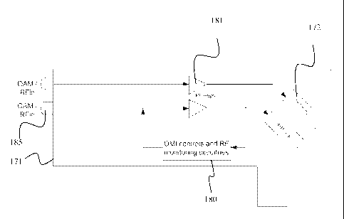
[027] Figure 3 illustrates an exemplary optical transmission unit 171 in
greater
detail. As illustrated in Figure 3, optical transmission unit 171 may be in
the form of a
card which may be inserted in a slot in the headend. Optical transmission unit
171
preferably contains a plurality of QAM/RF inputs 185 which may receive signals
from
CMTS 10, and a plurality of laser optical transmitters 172. The RF signals are
preferably
provided through RF amplifiers 181 to optical transmitters 172. An optical
modulation
interface (OMI) and RF monitoring circuits may control the RF levels and
modulation of
the laser in optical transmitters 172. Those of skill in the art will
appreciate that a laser in
optical transmitter 172 provides an optical signal at a specified fixed
frequency which is
modulated to carry the communication signals provided from CMTS 10.
[028] Figure 4 illustrates an exemplary circuit of an optical transmitter in
accordance with the principles of the invention. As illustrated in Figure 4,
the invention
includes a directed modulation laser 201, such as a laser modulated to provide
DWDM,
and a TEC driver 213 to set and maintain the laser temperature and the
operating channel
wavelength. Also included is an automatic power control circuitry (APC) 203 to
set bias
current and maintain constant output optical power, amplitude controller of
the dither
8
CA 02667646 2012-12-06
tone 217, a microcontroller 209 to control RF attenuation circuitry 207, the
bias current,
and the TEC driver 213. The microcontroller 209 may also provide serial ID
data and
digital monitoring for the output optical power, Itec and IBias current, etc.
and provide
data communication needed with the outside host module, such as transmission
unit 171.
An RF gain stage 205 with an RF attenuation capability at RF attenuator 207 is
preferably used to set the optical modulation index level of the laser
transmitter 201. An
exemplary RF attenuator is discussed in related application U.S. Publication
No.
2008095539 titled "Method And Apparatus For Controlling Channel Power Level In
A
Multi Channel System" filed on October 24, 2006.
[029] Laser 201 may be any suitable laser for optical communications, such as
a
continuous wave (CW) laser which may be directly modulated to provide the
communication signal. Preferably, laser 201 is a high power laser with low
chirp and
acceptable analog linear performance, e.g. noise power ratio (NPR) of 40/9 or
more, or a
modulation error ratio (MER) of 35 dB or more. For example, a 1.51,tm cooled
DFB 10
mW laser may be used, and may be a digital or analog laser. Laser 201 is
preferably in
the form of a laser diode contained in a transmitter optical subassembly
(TOSA), which
contains various components associated with the laser operations, such as a
thermistor to
monitor the laser temperature, a photodetector, a impedance matching resistor
and a
thermo-electric cooler (TEC) to cool the laser in response to instructions
from TEC driver
213. A suitable laser is a CW laser manufactured by NEC Electronics with model
no.
NX8530NH.
9
CA 02667646 2012-12-06
[030] As illustrated in Figure 4, an RF signal received from CMTS 10 is
provided to RF attenuator 207 where the amplitude level of the RF signal is
attenuated to
a desired level. The attenuated RF signal is provided to an amplifier 205
which may
increase the amplitude by providing gain. Pre-distortion circuitry 215
preferably corrects
for distortions, such as low frequency noise rise (LFNR), composite second
order (CS0),
composite triple beat (CTB) and cross modulation distortions, associated with
the RF
signal to provide the desired modulation of laser 201. Microcontroller 209,
illustrated
with a digital to analog converter (DAC) controls the RF attenuator 207, bases
on the
power detected by RF power detector 211. Microcontroller 209 also controls TEC
driver
213 which controls a thermo-electric cooler (not shown) which controls the
temperature
of laser 201. A dither tone 217 with amplitude level control may be imposed on
laser
201.
[031] Figure 5 illustrates an alternative implementation of optical
transmitter
172. As shown in Figure 5, the implementation is similar to that of Figure 4,
except that
the RF gain stage 205 and RF power detector are removed from optical
transmitter 172,
and are preferably placed at transmission unit 171. A microcontroller at the
host module
can communicate with the optical transmitter 172 and transfer serial ID and
monitoring
data. This alternative implementation may allow a higher level of OMI and
pluggable
tuned optics (TOSA) with all its electrical / optical parameters.
[032] Optical transmitter 172 preferably has low parasitic capacitance due to
its
short length and therefore it can achieve higher bandwidth and therefore
provides
capability of transmitting, for example, 256 QAM data or higher at distances
of 1001(m
or more over a single mode fiber in a small form pluggable cost effective
design. The
CA 02667646 2012-12-06
optical transmitter 172 is preferably capable of transmitting QAM modulated
optical
signal at output optical power up to 10 mw, for DWDM or CWDM system spacing
for
1.5 and 1.3 p.m application, also the design is preferably capable of
monitoring bias
current (i.e. Ibias), TEC current (i.e. ITec), and transmitted optical power.
[033] As illustrated in Figures 6-8, another important feature of the
invention is
allowing the user to fit many optical transmitters 172 on one small
transmission unit 171
as a host module (Figure 6), increasing the baud rate and transmitted
information through
the fiber. As illustrated in Figure 6, a plurality of optical transmitters 172
may be housed
in a housing 403 of transmission unit 171 by being inserted into receptacles
405.
Housing 403 may be secured to a headend unit 10 by insertion into a slot on
headend 14
(not shown). As illustrated in Figure 6, optical transmitters 172 preferably
contain a
receptacle for easy cabling with fiber optic lines as known to those of skill
in the art, such
as LC or SC type receptacles, or optical transmitter 172 may contain a pig
tail optical
connector (a short length of optical fiber projecting from it).
[034] Figure 7 illustrates a frontal view of optical transmitter 172 contained
in a
housing and Figure 8 illustrates a rear view of optical transmitter 172
contained in a
housing. As illustrated in Figures 7 and 8, optical transmitter 172 is
preferably
configured in a housing 501 that can be readily inserted and removed in a
receptacle in
transmission unit 171. In the preferred implementation, optical transmitter
172 may be
secured when inserted in transmission unit 171 by a bay latch 505 which
engages with a
notch on the housing of transmission unit 171 (not shown). Bay latch 505 may
be
actuated in a swinging motion or an in-out motion by an actuator rod 508 which
connects
to a handle 504, and moves bay latch 505 when handle 504 is moved. Handle 504
may
11
CA 02667646 2009-04-27
WO 2008/057904
PCT/US2007/083279
also be used to enable an operator to pull optical transmitter 172 out of the
receptacle in
transmission unit 171. In operation, pressing handle 504 against front face
506 of optical
transmitter housing 501 preferably engages latch 505 with optical transmission
unit
housing 403 to securely hold the optical transmitter 172. When handle 504 is
pulled,
such as when the arched end is rotated away from face 506 of housing 501,
latch 505 is
preferably disengaged, allowing optical transmitter 172 to be removed from
transmission
unit housing 403. While an arched shaped handle is illustrated for discussion
purposes,
those of skill in the art will recognize that any suitable handle shape may be
used,
including an irregular shaped handle. Those of skill in the art will
appreciate that the
invention allows an operator the capability to quickly and easily swap
transmitters and
change transmitter channels on a port by port basis.
[035] As illustrated in Figure 8, a rear face 507 of optical transmitter
housing
501 preferably contains a pin connector 503 which mates with a pin connector
in optical
transmission unit housing 403. Pin connector 503 may include a pin connector
with any
number of pins, such as a 20 pin electrical connector, or may include for
example, a SFP
XCVR edge connector. Control information, RF data signals and like are
preferably
provided to the optical transmitter 172 from the transmission unit 171 as the
host module.
[036] The optical transmitter 172, may utilize mechanical dimensions which
allow it to utilize existing packages or replace existing structures. For
example, the
optical transmitter 172 may use the dimensions of the SFP telecom transceivers
specified
in the SFP multi source agreement (MSA), e.g. (H x W x D) = 8.6 x 13.7x 56.6
mm. The
transmission unit 171, as a host module at the head end could be designed to
hold 16, 32,
40, etc. of the optical transmitters 172. Those of skill in the art will
appreciate that use of
12
CA 02667646 2009-04-27
WO 2008/057904
PCT/US2007/083279
a large number of optical transmitters 172 in a transmission unit 171 not only
uses an
operator's available space more efficiently, it also increase the transmission
data capacity
by providing the operator the ability to transmit all DWDM wavelength channels
using a
single host module panel that fits the large number of optical transmitters
172.
[037] The small form factor of the optical transmitter 172 provides a cost
effective solution. Since the operator can densely pack more than 40 optical
channels in
a single optical transmission unit, the operator can transmit QAM data in a
very efficient
matter, such as with low cost and high data capacity per chassis volume. The
pluggable
nature of the optical transmitter 172 also allows an operator to easily remove
and swap
one optical transmitter for another in event of a desired channel change or an
optical
transmitter becomes defective or damaged by just removing the optical
transmitter from
the host module cages. The invention also allows the operator of the HFC
network to
combine multiple optical transmitters in a smaller host module reside at the
head end or
at the hub or at the node to transmit data at many different wavelengths from
the same
host module.
13