Note: Descriptions are shown in the official language in which they were submitted.
CA 02670073 2009-05-14
WO 2008/133656 PCT/US2007/024043
NANOSCALE SENSORS
STATEMENT REGARDING FEDERALLY-SPONSORED RESEARCH OR
DEVELOPMENT
CROSS-REFERENCE TO RELATED PATENT APPLICATIONS
[0001] This application claims priority from U.S. Provisional Application
Number
60/859,735, filed 11/17/2006, incorporated herein by reference in its
entirety.
BACKGROUND OF THE INVENTION
[0002] The present invention relates generally to the field of nanoscale
sensors, and
more particularly to an apparatus and method for detecting a target species
using
nanoscale sensors.
[0003] Chemical and biological sensors typically operate at elevated
temperatures to
enhance chemical reactivity, and often require long recovery times (if
recoverable at
all), poor reproducibility, and are applicable to the detection of a very
limited range of
chemical and biological species and are described in U.S. Patent No.
7,013,708,
entitled "Carbon Nanotube Sensors"; U.S. Patent No. 7,166,325, entitled
"Carbon
Nanotube Devices"; U.S. Application Publication No. 2003/0134267, entitled
"Sensor
for Detecting Biomolecule Using Carbon Nanotubes"; U.S. Application
Publication
No. 2004/0245209, entitled "Method for Fabricating a Carbon Nanotube Array and
a
Biochip Using the Self-Assembly of Supramolecules and Staining of Metal
Compound"; U.S. Application Publication No. 2005/0181409, entitled "Biochip
and
Biomolecular Detection System Using the Same"; and U.S. Patent Application
Publication No. 2005/0230270, entitled "Carbon Nanotube Nanoelectrode Arrays."
[0004] An article by Choi et al., entitled "YY1-DNA interaction results in a
significant change of electronic context as measured by capacitance,"
Biophysical
-1-
CA 02670073 2009-05-14
WO 2008/133656 PCT/US2007/024043
Chemistry 103, 109-115 (2003), which is incorporated herein by reference in
its
entirety, describes a nanosensor that detects a dielectric change upon the
formation of
a specific Yin-Yang 1(YYl)-DNA complex within an 80-nm gap between two
electrodes of a capacitor. Aliquots of a mixture of YYI and P5 promoter DNA
were
placed on the capacitor and, after a 5-min incubation period, the capacitance
was
measured between 10 kHz and 3 MHz. Changes in the capacitance were attributed
to
the specific YYI-DNA complexation. It is believed that the dielectric effect
is due to
the alignment of dipoles to the electric field of the capacitor, whereby a
stronger
dipole results in greater capacitance. However, the sensitivity of the device
suffered
due to signal contributions arising from complexation and other contributions
outside
of the electrode gap.
SUMMARY OF THE INVENTION
[0005] One embodiment of the invention provides a nanosensor that includes a
capacitor having a nanocavity between a first and second conductor of the
capacitor.
The nanosensor is adapted to exhibit each of a size-dependent physical
selection of
target species entering into the nanocavity, a selective capture of at least
one of the
target species within the nanocavity to at least one of the first and second
conductors;
and an electromagnetic shielding within the nanocavity such that a signal
produced in
response to the selective capture within the nanocavity is substantially
undisturbed by
a capture outside of the nanocavity.
[0006] Another embodiment of the invention provides a nanocoaxial sensor that
includes an outer conductor, an inner conductor, a nanocavity sized to allow
target
species to enter the nanocavity between the outer and inner conductors, and an
active
sensing element immobilized within the nanocavity on at least one of the inner
or
outer conductors. The active sensing element is adapted to selectively capture
at least
one of the target species.
[0007] Another embodiment of the invention provides a method of making a
nanocoaxial sensor. The method includes providing an array of vertically-
aligned
nanostructures grown substantially perpendicular to a substrate, wherein each
-2-
CA 02670073 2009-05-14
WO 2008/133656 PCT/US2007/024043
nanostructure is circumferentially surrounded by a dielectric material
disposed within
a metal cylinder, and forming at least one nanocavity by removing at least a
portion of
the dielectric material located on a side of the array opposite the substrate.
[0008] Another embodiment of the invention provides a method of using a
nanosensor to detect a presence of a target species. The method includes
transmitting
electromagnetic waves through a medium disposed between a first and second
electrode of the nanosensor, wherein the first and second electrodes comprise
an inter-
electrode spacing of no more than about 500 nm and the waves are substantially
shielded by the first and second electrodes, and monitoring for a change in
the
electromagnetic waves based on a change in a dielectric constant between the
first and
second electrodes, wherein the change in the dielectric constant corresponds
to the
presence of the target species between the first and second electrodes.
BRIEF DESCRIPTION OF THE DRAWINGS
[0009] FIG. lA shows a schematic image of a nanoscale sensor unit structure
according to an embodiment of the present invention.
[0010] FIG. 1 B shows an equivalent circuit diagram of the nanoscale sensor
unit
structure of FIG. 1 A.
[0011] FIG. 2A-2C show schematic and exemplary views of a nanoscale coaxial
transmission line built around a carbon nanotube. FIG. 2A shows a schematic
view
and an exemplary view of a carbon nanotube. FIG. 2B shows a schematic view and
an exemplary view of the carbon nanotube in FIG. 2A after coating with a
dielectric
material. FIG. 2C shows a schematic view and an exemplary view of the carbon
nanotube in FIG. 2B after coating with an outer conductor material.
[0012] FIG. 3A shows a schematic view of a nanoscale coaxial transmission line
built around a carbon nanotube. FIG. 3B shows a scanning electron microscope
(SEM) image of the nanoscale coaxial transmission line built around a carbon
nanotube. The carbon nanotube's diameter is about 100 nm.
-3-
CA 02670073 2009-05-14
WO 2008/133656 PCT/US2007/024043
[0013] FIG. 4 shows the plasmon polariton dispersion co(k) at the metal-
dielectric
interface of a nanoscale coaxial transmission line according to an embodiment
of the
present invention.
[0014] FIG. 5 shows a nanoscale coaxial transmission line array according to
an
embodiment of the present invention. FIG. 5A shows a single nanoscale coaxial
transmission line viewed by SEM. FIG. 5B shows a cross-section view of a
single
nanoscale coaxial transmission line viewed by a scanning electron microscope.
FIG.
5C shows an energy dispersive x-ray spectroscopy (EDS) analysis of the
composition
of the coaxial layers showing concentration mapping for silicon (Si), chromium
(Cr),
and aluminum (Al).
[0015] FIG. 6A-6G show the results of a small-area reflection and transmission
experiment of a nanoscale coaxial transmission line according to an embodiment
of
the present invention. FIG. 6A shows a high-resolution optical microscope
image of
white light reflected from the nanoscale coaxial transmission line medium.
FIG. 6B
shows a high-resolution optical microscope image of white light transmitted
through
the medium. FIG. 6C is an SEM image of the nanoscale coaxial transmission line
medium surface (tilted 45 deg). FIGS. 6A-6C have the same magnification. FIG.
6D
shows an image of a laser beam with A= 532 nm transmitted through a glass
substrate
(exposure time 0.0025 sec). FIG. 6E shows an image of a laser beam with X= 532
nm
transmitted through the nanoscale coaxial transmission line medium on the same
glass
substrate (exposure time 1 sec). FIG. 6F shows an image of a laser beam with
X= 680
nm transmitted through a glass substrate (exposure time 0.0025 sec). FIG. 6G
shows
an image of a laser beam with X= 680 nm transmitted through the nanoscale
coaxial
transmission line medium on the same glass substrate (exposure time 1 sec).
FIGS.
6D-6G have the same magnification.
[0016] FIG. 7 shows SEM images of the cross-section of the nanoscale coaxial
transmission line medium at different transmission line lengths: 6 m (FIG.
7A), 3.5
m (FIG. 7B), and 0.4 m (FIG. 7C). FIG. 7D shows a plot of ineasured intensity
of
the transmitted light at fixed wavelength (X= 532 nm) versus sample thickness.
-4-
CA 02670073 2009-05-14
WO 2008/133656 PCT/US2007/024043
[0017] FIG. 8A-8B show a nanocoaxial sensors according to an embodiment of the
present invention.
[0018] FIG. 9A-9F show the steps used for fabricating a nanoscale sensor
according
to an embodiment of the present invention.
[0019] FIG. 10 shows a complex impedance (Nyquist) plot of a nanoscale sensor
immobilized with goat anti-human antibody and the response to antigen, human
IgG,
binding. Trace a and b are the results before and after IgG binding.
100201 FIG. I 1 shows a dielectric permittivity spectrum over a wide range of
frequencies. The real and imaginary parts of permittivity are shown, and
various
processes are depicted: ionic and dipolar relaxation, and atomic and
electronic
. resonances at higher energies.
[0021] FIG. 12 shows an experimental setup of an Impedance Spectroscopy (IS)
apparatus that may be used with the nanoscale ultrasensitive sensor unit
structure
according to an embodiment of the present invention.
[0022] FIG. 13 shows a simplified block diagram of the set-up common for most
Time Domain Dielectric Spectroscopy (TDDS) methods.
100231 FIG. 14 shows the characteristic shape of the signals recorded during a
TDDS experiment as shown in FIG. 13.
[0024] FIG. 15A-15D are SEM images showing the steps used to fabricate an
array
of nanocoaxial sensors according to an embodiment of the present invention.
[0025] FIG. 16A-16D show an individually-addressable array of nanocoaxial
sensors according to an embodiment of the present invention.
[0026] FIG. 17 are SEM images showing the tunability of the size of the
nanocavity
openings of the nanocoaxial sensors according to an embodiment of the present
invention.
[0027] FIG. 18A-18C shows gold film nucleation and CNT functionalization
according to an embodiment of the present invention. FIG. 18A is a schematic
diagram of an experimental setup used to nucleate a gold film. FIG. 18B is a
plot of
-5-
CA 02670073 2009-05-14
WO 2008/133656 PCT/US2007/024043
resistivity versus temperature of the gold film. FIG. 18C shows the steps of a
method
for functionalizing CNTs with gold nanoparticles according to an embodiment of
the
present invention.
[0028] While the above-identified drawings set forth presently disclosed
embodiments, other embodiments are also contemplated, as noted in the
discussion.
This disclosure presents illustrative embodiments by way of representation and
not
limitation. Numerous other modifications and embodiments can be devised by
those
skilled in the art which fall within the scope and spirit of the principles of
the
presently disclosed embodiments.
DETAILED DESCRIPTION OF THE PREFERRED EMBODIMENTS
[0029] The embodiments disclosed herein relate to the field of nanoscale
sensors,
and more particularly to an apparatus and method for ultrasensitive sensing of
target
species, such as chemical and/or biological molecules, using nanoscale
sensors.
Methods of fabricating a nanoscale sensor apparatus are also disclosed. The
nanoscale sensors are able to capture the real-time signals from a single
target species.
The nanoscale sensors may be used in various biomedical related applications
including, but not limited to, clinic diagnosis, bio-attack alarming system,
drinking
water monitoring, biomolecule characterization in research, constructing an
artificial
neuronal post-synaptic membrane, food quality test, allergic species
detection,
forensic examination, and personnel biological identification. The nanoscale
sensors
may be used in various non-biomedical areas including, but not limited to,
explosive
detection, narcotics control, and pollution monitoring.
[0030] The basic elements of nanoscale capacitance sensor measurements are
disclosed. The nanoscale sensors are used to detect particles of bio-species,
for
example, with ultrasensitivity that affords single molecule detection. The
nanoscale
sensor unit structure comprises a dielectric material located between a first
electrical
conductor and a second electrical conductor. The nanoscale sensor unit
structure
constitutes a nanoscale capacitor and forms a nanoscale coaxial transmission
line built
around an internal conductor with the diameter registered at any value between
about
-6-
CA 02670073 2009-05-14
WO 2008/133656 PCT/US2007/024043
1 nm and about 1000 nm, such as about 40 nm to about 200 nm, for example about
100 nm. Biomolecules, or biologically active sensing elements, are immobilized
either on the first conductor or the second conductor, or both.
[00311 The following definitions are used to describe the various aspects and
characteristics of the presently disclosed embodiments.
[0032] As used herein, "nanostructures" and "nanostructure materials" refer to
a
broad class of materials, with microstructures modulated in zero to three
dimensions
on length scales less than about 1,000 nm; materials with atoms arranged in
nanosized
clusters, which become the constituent grains or building blocks of the
material; and
any material with at least one dimension in the about 1-1,000 nm range. Using
a
variety of synthesis methods, it is possible to produce nanostructured
materials in the
following forms: nanorods, nanowires, nanopillars, nanofibers, nanotubes,
nanohoms, thin films, coatings, powders and as a bulk material. In an
embodiment,
the material comprising the nanostructure is carbon. In an embodiment, the
material
comprising the nanostructure need not be carbon. In applications where
symmetric
structures are generated, the sizes (largest dimensions) can be as large as
tens of
microns.
[0033] As used herein, "carbon nanotubes" and "CNTs" are used interchangeably.
These terms primarily refer to a type of carbon nanofiber having cylindrical
carbon
molecules. CNTs may have unique properties that make them potentially useful
in a
wide variety of applications in nanotechnology, electronics, optics, and other
fields of
materials science. They exhibit extraordinary strength and unique electrical
properties, and are efficient conductors of heat.
[0034] As used herein, "single-walled carbon nanotubes" (SWCNTs) are made of
one graphene sheet rolled into a cylinder. "Double-walled carbon nanotubes"
(DWCNTs) are made of two graphene sheets in parallel, and those with multiple
sheets (typically about 3 to about 30) are "multi-walled carbon nanotubes"
(MWCNTs). For the coaxial nanostructures disclosed herein, MWCNTs need not be
specifically graphitic (i.e. crystalline graphene) in structure, but can be
fibrous.
-7-
CA 02670073 2009-05-14
WO 2008/133656 PCT/US2007/024043
MWCNTs are a type of carbon nanotube, and carbon nanotubes are a type of
carbon
nanofiber.
[0035] As used herein, a CNT is "vertically aligned" when its longitudinal
axis is
oriented substantially perpendicular to a substrate on which the CNT's
proximal end
is in contact, for example the substrate from which the CNT is grown. CNTs may
be
vertically aligned even if they are not exactly perpendicular to the substrate
and even
if they are curved or kinked.
[0036] As used herein, a "tubule" is an individual CNT.
[0037] As used herein, "linear CNTs" refer to CNTs that do not contain any
branches originating from the surface of individual CNT tubules along their
linear
axes.
[0038] As used herein, "conductor" refers to an electrically conducting
material. A
conductor may be a metallic or non-metallic material.
[0039] As used herein CNTs have a"uniform length" wherein the length of
individual tubules are substantially the same length relative to one another.
Depending on growth conditions used, the height of a CNT in an array in a
given
growth run can be varied in height by about 10% to about 50%. Alternatively,
height
uniformity is accomplished by performing additional mechanical polish steps.
In an
embodiment, the CNTs have a uniform length from about 1 to about 50
micrometers.
[0040] As used herein, the "aspect ratio" of a CNT is the ratio of tubule
length and
tubule diameter.
[0041] The CNTs have "proximal" and "distal" ends. The proximal ends of the
CNTs engage a substrate.
[0042] As used herein, a"nanoscale coaxial transmission line" refers to a
nanoscale
coaxial wire, which includes a plurality of concentric layers. In an
embodiment, the
nanoscale coaxial transmission line has three concentric layers: an internal
conductor,
a dielectric material around the internal conductor, and an outer conductor.
Transmission of electromagnetic energy inside the coaxial line is wavelength-
independent and happens in transverse electromagnetic (TEM) mode. In an
-8-
CA 02670073 2009-05-14
WO 2008/133656 PCT/US2007/024043
embodiment, the internal conductor is a metallic core. In an embodiment, the
outer
conductor is a metallic shielding that increases the signal-to-noise ratio of
the detected
signal.
[0043] As used herein, a "nanoscale coplanar line" refers to a nanoscale
coplanar
structure, which includes a plurality of parallel layers. In an embodiment,
the
nanoscale coplanar line has three parallel layers: two metallic conductors,
with a
dielectric coating between them. Transmission of electromagnetic energy inside
the
coplanar line is wavelength-independent and happens in transverse
electromagnetic
(TEM) mode.
[0044] As used herein, "transverse electromagnetic (TEM)" refers to an
electromagnetic mode in a transmission line for which both the electric and
magnetic
fields are perpendicular to the direction of propagation. Other possible modes
include
but are not limited to transverse electric (TE), in which only the electric
field is
perpendicular to the direction of propagation, and transverse magnetic (TM),
in which
only the magnetic field is perpendicular to the direction of propagation.
[0045] As used herein, "nano-optics" is the study of optical interactions with
matter
on a subwavelength scale, i.e., nanoscale optics.
[0046] As used herein, an "optical signal" refers to any electromagnetic
radiation
pulse including gamma rays, X-rays, ultraviolet light, visible light,
infrared,
microwaves, radio waves (ULF, VLF, LF, MF, HF, long, short, HAM, VHF, UHF,
SHF, EHF), cosmic microwave background radiation and other forms of radiation
of
the electromagnetic spectrum.
[0047] As used herein, a "non-metallic material" is any non-conductive
material
suitable for depositing a metallic layer thereupon. Examples of "non-metallic
materials" include but are not limited to, silicon, silica, glass, alumina,
quartz,
polymer and graphite. Examples of non-metallic polymers include but are not
limited
to, polyvinyl chloride (PVC), polyacrylate (PA), polypropylene (PP),
polyphenol
(PPN), polymethylmethacrylate (PMMA), polycarbonate (PC), polyethylene (PE)
and
thermoset plastics. In an embodiment, the non-metallic material is a silicon
wafer.
-9-
CA 02670073 2009-05-14
WO 2008/133656 PCT/US2007/024043
[0048] As used herein, a "metallic material" can be a metal, metal alloy or
mixture
thereof. Examples of a metallic material include, but are not limited to,
chromium
(Cr), molybdenum (Mo), tungsten (W), ruthenium (Ru), copper (Cu), silver (Ag),
gold (Au), and conductive polymers. In an embodiment, the metallic material is
chromium (Cr).
[0049] As used herein, a "catalytic transition metal" can be any transition
metal,
transition metal alloy or mixture thereof. Examples of a catalytic transition
metal
include, but are not limited to, nickel (Ni), silver (Ag), gold (Au), platinum
(Pt),
palladium (Pd), iron (Fe), ruthenium (Ru), osmium (Os), cobalt (Co), rhodium
(Rh)
and iridium (Ir). In an embodiment, the catalytic transition metal comprises
nickel (Ni).
[0050] As used herein, a "catalytic transition metal alloy" can be any
transition
metal alloy. Preferably, a catalytic transition metal alloy is a homogeneous
mixture or
solid solution of two or more transition metals. Examples of a catalytic
transition
metal alloy include, but are not limited to, a nickel/gold (Ni/Au) alloy and a
cobalt/iron (Co/Fe) alloy.
[0051] In an embodiment, a working electrode is a metallic coated non-metallic
substrate for use in depositing a catalytic transition metal. In an embodiment
the
working electrode is a chromium (Cr) coated silicon (Si) wafer. The chromium
(Cr)
coating provides a flat, conductive and defect free surface on the silicon
(Si) wafer. A
method of preparing a chromium (Cr) coated silicon (Si) wafer comprises
sputtering a
layer of chromium (Cr) on a silicon (Si) wafer. In an embodiment the
sputtering
method is magnetron sputtering.
[0052] In an embodiment, a counter electrode is any suitable electrically-
conductive
metal. In an embodiment, the counter electrode comprises a noble metal:
Examples
of suitable noble metals include, but are not limited to, gold (Au), platinum
(Pt) and
iridium (Ir). In an embodiment, the counter electrode is gold (Au) plate.
[0053] In an embodiment, an electrolytic solution is a transition metal salt
and a
mineral acid. Preferably, the transition metal salt is a transition metal
sulfate. In an
embodiment, the transition metal sulfate is nickel sulfate (NiSO4). Examples
of
-10-
CA 02670073 2009-05-14
WO 2008/133656 PCT/US2007/024043
suitable mineral acids include but are not limited to boric acid (H3B03),
nitric
acid (HNO3), hydrochloric acid (HC1) and sulfuric acid (H2SO4). Preferably the
electrolytic solution is weekly acidic. In an embodiment, the mineral acid is
boric
acid (H3BO3). For example, the electrolytic solution comprises 0.01 M nickel
sulfate
(NiSO4) and 0.01 M boric acid (H3B03) in double distilled water.
[0054] Pulse-Current Electrochemical Deposition (PCED) is an electrochemical
deposition process which utilizes a modulated current waveform (a current
pulse).
PCED can be used to achieve superior leveling of the deposit, and to minimize
porosity and contamination. PCED is performed by applying a constant current
pulse
by using a current source and a voltage source. Both the current source and
the
voltage source are controlled by any suitable means known in the art including
analog
and digital controller devices. In an embodiment, the current source and the
voltage
source is controlled by a computer. In an embodiment, PCED is performed by
applying a constant current pulse to a two electrode system comprising a
working
electrode and a counter electrode. The working electrode and the counter
electrode
are spaced at a suitable distance. In an embodiment, PCED is carried out on a
two
electrode system, wherein the distance between the two electrodes is
maintained at
about 1 cm, and a constant current pulse is applied by using a current source
and a
voltage source, both of which are controlled by the computer program. The
working
electrode is prepared by sputtering a layer of chromium on a silicon wafer
thereby
obtaining a flat, conductive and defect free surface. A gold plate is used as
a counter
electrode. About 1 cm2 of the working electrode surface is exposed to a weakly
acidic
electrolyte solution comprising 0.01 M NiSO4 (0.O1M Niz+) and 0.01 M H3B03 in
double distilled water at room temperature. PCED is performed at any suitable
temperature. In an embodiment, the PCED is performed at room temperature.
[0055] Many factors with PCED can affect the deposited microparticles,
including
the composition of the electrolyte solution; the surface morphology of the
substrate;
the magnitude of the applied pulse current density and the duration time.
Lowering
the concentration of transition metal ions will decrease both the nucleation
site density
and the size of the deposited catalytic transition metal microparticles.
-11-
CA 02670073 2009-05-14
WO 2008/133656 PCT/US2007/024043
[0056] Varying mineral acid concentrations, such as boric acid concentrations,
changes the pH value. Solutions with a support electrolyte (potassium
chloride)
added are tested and it is found only when the concentration of mineral acid
is very
low and no other support electrolyte is added, the catalytic transition metal -
microparticles with low site density and large size (larger than 100 nm in
diameter)
are achieved. When the mineral acid concentration increases or some other
support
electrolyte is added, the conductivity of the solution increases, and the
electrodeposited catalytic transition metal microparticles have higher density
and
smaller size. The surface morphology of the substrate also affects the
distribution of
the deposited catalytic transition metal microparticles. Microparticles form
on the
defect site of the substrate with high site density. In order to eliminate the
aggregation of the microparticles, a sputtering method is used to coat a thin
layer of
metallic material such as chromium (Cr) on the non-metallic substrate material
such
as a silicon (Si) wafer to obtain a conductive and defect free surface.
[0057] When the solution composition and the substrate are fixed, the site
density
and the size of the catalytic transition metal microparticles are determined
by the
combined effect of applied pulse current density and duration time. High
current
density and long duration time result in high site density and large particles
(greater
than about 100 nm).
[0058] In an embodiment, the size distribution of the electrochemical
deposited
catalytic transition metal microparticles is quite large. Both large particles
(greater
than about 100 nm) and small particles (less than about 50 nm) are deposited
on the
substrate material. The morphology of the CNTs is related to the size of the
catalytic
transition metal microparticles. When the diameter of the catalytic transition
metal
microparticles is smaller thanabout 50 nanometers, either no CNTs or only
short and
curved CNTs are grown. When the size of the catalytic transition metal
microparticles is large, well-aligned CNTs with uniform length distribution
are
grown. In an embodiment, the substrate material is optionally plasma etched
prior to
CNT growth to substantially reduce the number of catalytic transition metal
microparticles that have a diameter smaller than about 50 nanometers. The
plasma
etches the catalyst substrate and at the same time assists the CNT growth.
-12-
CA 02670073 2009-05-14
WO 2008/133656 PCT/US2007/024043
[0059] CNTs can be grown by any suitable method known in the art. For example,
CNTs can be grown by any chemical vapor deposition (CVD) method, including but
not limited to, plasma enhanced chemical vapor deposition (PECVD), hot
filament
chemical vapor deposition (HFCVD) or synchrotron radiation chemical vapor
deposition (SRCVD). In CVD, gaseous mixtures of chemicals are dissociated at
high
temperature (for example, CO2 into C and 02). This is the "CV" part of CVD.
Some
of the liberated molecules may then be deposited on a nearby substrate (the
"D" in
CVD), with the rest pumped away. In an embodiment, CNTs are obtained by
placing
a catalyst substrate material, which is formed by electrochemical deposition
of
catalytic transition metal microparticles, with a pre-determined site density,
on a
metal coated non-metallic substrate material, within a PECVD chamber known in
the
art, following which CNT growth is initiated on the surface of the catalyst
substrate
material by standard methods described in the art (see for example Z. F. Ren,
et al.,
Science, 282, 1105 (1998); Z. P. Huang, et al., Appl. Phys. A: Mater. Sci.
Process, 74,
387 (2002); and Z. F. Ren et al., Appl. Phys. Lett., 75, 1086 (1999), all of
which are
incorporated herein by reference in their entirety).
[0060] A promoter gas can be a substance that is a gaseous compound at the
reaction temperatures, and preferably comprises a non-carbon gas such as
ammonia,
ammonia-nitrogen, hydrogen, thiophene, or mixtures thereof. The promoter gas
may
be diluted by mixing it with a diluent gas, which are primarily unreactive,
oxygen-free
gases, such as for example, hydrogen, helium, nitrogen, argon, neon, krypton,
xenon,
hydrogen sulfide, or combinations thereof. For the CVD reaction process of the
presently disclosed embodiments, hydrogen is preferred for reaction
temperatures
maintained at less than about 700 C, while for higher temperatures (greater
than or
equal to about 700 C), the promoter gas is chosen from ammonia, hydrogen,
nitrogen,
or any combination thereof. The promoter gas can be introduced into the
reaction
chamber of the reaction apparatus (e.g. the CVD reaction chamber) at any stage
of the
reaction process. Preferably, the promoter gas is introduced into the reaction
chamber
either prior to or simultaneously with the carbon source gas. The CNT nanotube
nucleation process on the catalyst substrate is catalyzed by the promoter gas
enabling
-13-
CA 02670073 2009-05-14
WO 2008/133656 PCT/US2007/024043
every metal catalyst "cap" that is formed within individual tubules to
catalyze their
efficient and rapid growth.
[0061] A carbon source gas can be saturated, unsaturated linear branched or
cyclic
hydrocarbons, or mixtures thereof, that are in either the gas or vapor phase
at the
temperatures at which they are contacted with the catalyst substrate material
(reaction
temperature). Preferred carbon source gases include methane, propane,
acetylene,
ethylene, benzene, or mixtures thereof. In an embodiment, the carbon source
gas for
the synthesis of linear CNTs is acetylene.
[0062] CNT tubule diameter, tubule length, number of concentric graphene
layers
(graphitization) comprising individual tubules and the yield of the CNTs is
controlled
by varying the reaction temperature of CNT synthetic process.
[0063] The manufacturing methods described herein facilitate the tailoring of
linear
CNT morphology by controlling gas pressure. At low pressures, CNTs with a
tubular
hollow structure can be obtained, whereas at high pressures, CNTs with "bamboo-
like" structure and increased compartmental density can be obtained. The
number of
graphene layers, which is related to thickness of the tubule wall and
diaphragm of the
CNTs, can also be controlled during their formation by control of gas
pressure. Once
the first layer forms as a bamboo-like structure, all subsequent layers
terminate on the
surface of the CNT.
[0064] Scanning electron microscopy (SEM) is employed to examine the
morphology. Transmission electron microscopy (TEM) is used to characterize the
structure of the CNTs by standard methods.
[0065] A dielectric can be any a non-conducting or insulating material.
Preferably,
the dielectric has a low porosity, a high density and is substantially defect
free.
Examples of dielectrics include high-density polymers, and metal oxides. In an
embodiment, the dielectric is aluminum oxide (A1203), Si02, MgO, Si3N4 or
Ti02, or
a combination thereof.
[0066] As used herein, the term "ligand" or "analyte" or "marker" or "target
species" refers to any molecule being detected. It is detected through its
interaction
-14-
CA 02670073 2009-05-14
WO 2008/133656 PCT/US2007/024043
with an active sensing element, which specifically or non-specifically binds
the target
species. The target species can be any molecule for which there exists another
molecule, such as an active sensing element, which specifically or non-
specifically
binds to the target species, owing to recognition, chemical or otherwise, of
some
portion of the target species. The active sensing element, for example, can be
an
antibody and the target species a molecule such as an antigen which binds
specifically
to the antibody. In the event that the antigen is bound to the surface and the
antibody
is the molecule being detected, for the purposes of this document the antibody
becomes the target species and the antigen is the active sensing element. The
target
species may include nucleic acids, proteins, lipids, small molecules,
membranes,
carbohydrates, polymers, cells, cell membranes, organelles and synthetic
analogues
thereof.
[0067] Target species include, but are not limited to, antibodies (forming an
antibody/epitope complex), antigens, nucleic acids (e.g. natural or synthetic
DNA,
RNA, gDNA, cDNA, mRNA, tRNA, etc.), lectins, sugars (e.g. forming a
lectin/sugar
complex), glycoproteins, receptors and their cognate target species (e.g.
growth
factors and their associated receptors, cytokines and their associated
receptors,
signaling receptors, etc.), small molecules such as drug candidates (either
from natural
products or synthetic analogues developed and stored in combinatorial
libraries),
metabolites, drugs of abuse and their metabolic by-products, co-factors such
as
vitamins and other naturally occurring and synthetic compounds, oxygen and
other
gases found in physiologic fluids, cells, cellular constituents cell membranes
and
associated structures, natural or synthetic toxins, pathogens (e.g., Bacillus
anthracis,
Yersinia pestis, Francisella tularensis, Coxiella bumetii) other natural
products found
in plant and animal sources, other partially or completely synthetic products,
pathogens (e.g. virus and bacteria, etc.), and the like. Target species may be
found in a
variety of heterogeneous test samples (e.g., water, saliva, sweat, urine,
serum, blood,
plasma, tissues and food).
[0068] The active sensing element is adapted to selectively capture at least
one
target species. For example, the active sensing element can specifically or
nonspecifically bind with another molecule (such as a target species). Also,
the active
-15-
CA 02670073 2009-05-14
WO 2008/133656 PCT/US2007/024043
sensing element can exert specific enzymatic activity with the target species
to
produce intermediate molecules that can change the physiochemical environment
in
the nanocavity. As used herein, the active sensing element is usually
immobilized on
the surface of a nanoscale sensor, either alone or as a member of a binding
pair that is
immobilized on the surface. In some embodiments, the active sensing element
may
include the molecules on the signal path, on a dielectric surface or in a
dielectric
volume, or a conductive surface, such as on the inner or outer conductor of
the coaxial
nanosensor. Immobilization of the active sensing element can be performed by
one or
more linkers.
[0069] The selective capture of the target species can be a specific binding,
such as
by a binding reaction which is determinative of the cognate target species of
interest
in a heterogeneous population of proteins and/or other biologics. Thus, under
designated conditions, the specified target species binds to its particular
active sensing
element (e.g., a hormone specifically binds to its receptor, or a given
nucleic acid
sequence binds to its complementary sequence) and does not bind in a
significant
amount to other molecules present in the sample or to other molecules to which
the
target species or antibody may come in contact in an organism or in a sample
derived
from an organism.
[0070] FIG. lA shows a schematic view of a nanoscale sensor unit structure
100.
The nanoscale sensor unit structure 100 comprises a dielectric material
1801ocated
between a first electrical conductor 120 and a second electrical conductor
160. The
first electrical conductor 120 serves as an internal electrode and the second
electrical
conductor 160 serves as an outer electrode. The nanoscale sensor unit
structure 100 is
supported by a metallized substrate 190, such as an insulating or
semiconducting
substrate that is partially or entirely coated with a metal layer. Other
substrates,
including substrates without a metal layer, may be used. The standing
nanoscale
sensor unit structure 100 is supported by a thick dielectric material 140. A
nanocavity
130 is fabricated at the upper end of the nanoscale sensor unit structure 100
after
chemical etching of at least a portion of the dielectric material 180. In an
embodiment, the dielectric material 180 is entirely removed by etching.
Alternatively, a portion of the dielectric material 180 is removed by etching.
In an
-16-
CA 02670073 2009-05-14
WO 2008/133656 PCT/US2007/024043
embodiment, the dielectric material is A1203 and is etched with NaOH. Active
sensing elements 150 can be immobilized within the nanocavity 130, for example
on
the first electrical conductor 120 for selective capture of the target
species. The
nanocavity area houses a solution containing the target species. In an
embodiment,
the solution may be aqueous based, such as pure water, water with bio-
molecules,
physiological saline or other solutions known in the art. In an embodiment,
the
solution may be in organic solvents, such as acetic acid, acetone, benzene,
carbon
tetrachloride, chloroform, dichloromethane, dimethylformalmide (DMF),
dimethylsulphonate (DMSO), ethanol, ether, ethyl acetate, light petroleum,
methylated spirits (-2% methanol in ethanol), methanol, petroleum spirit,
pyridine,
mineral oil, or other solvents known to those skilled in the art.
[0071] The internal electrode 120 may be a nanostructure having a conductive
core.
Examples of materials that can be used for the internal electrode 120 include
but are
not limited to, carbon fiber; carbon nanotube; pure transition metals such as
nickel
(Ni), aluminum (Al), or chromium (Cr); metal alloys, e.g. stainless steel
(Fe/C/Cr/Ni)
or aluminum alloys (Al/Mn/Zn); and metallic polymers. Other internal
electrodes 120
are highly doped semiconductors, and semi-metals (metals with vanishingly
small
band gap, e.g. graphite). In an embodiment, the internal electrode 120 is a
carbon
nanofiber, such as carbon nanotube, for example a SWCNT or MWCNT. The
nanotubes may, but need not, be substantially of the metallic chirality. The
nanotubes
can include a mixture of metallic and semiconducting chiralities. The
nanotubes are
preferably sufficiently conductive to be used as the inner conductor of a
nanocoaxial
capacitor. Those skilled in the art will recognize that the internal electrode
120 may
be other conducting materials known in the art and be within the spirit and
scope of
the present embodiments.
[0072] The dielectric material 180 circumferentially surrounds a portion of
the
internal electrode 120, either uniformly surrounding the internal electrode
120 or non-
uniformly surrounding the internal electrode 120. In an embodiment, the
dielectric
material 180 may be A1203i Si02, MgO, Si3N4 TiO2, or a non-conductive polymer,
or
a combination thereof, and may be deposited by sputter coating, atomic layer
deposition, or electropolymerization. The dielectric material 180 can be
crystalline
-17-
CA 02670073 2009-05-14
WO 2008/133656 PCT/US2007/024043
(periodic arrangement of atoms in macroscopic scale), polycrystalline
(periodic
arrangement of atoms in microscopic scale), or amorphous (aperiodic
arrangement of
atoms in macroscopic scale). Optionally, the dielectric material 180 can be
omitted.
[0073] The second electrical conductor or outer electrode 160 may be a metal
nanostructure. Thus, the outer electrode 160 may take the form of a metallic
cylinder.
In an embodiment, the metallic cylinder provides shielding of electromagnetic
waves
that are transmitted along the length of the unit structure 100. Examples of
outer
electrodes include but are not limited to, pure transition metals such as
nickel (Ni),
aluminum (Al), chromium (Cr), titanium (Ti), gold (Au), platinum (Pt); metal
alloys
e.g. stainless steel (Fe/C/Cr/Ni) or aluminum alloys (Al/Mn/Zn); a conductive
metal
oxide; and metallic polymers. In an embodiment the outer electrode 160 is
chromium. Those skilled in the art will recognize that the outer electrode 160
may be
other conducting materials known in the art and be within the spirit and scope
of the
presently disclosed embodiments.
[0074] The nanoscale sensor unit structure 100 can be simplified as a
nanoscale
coaxial capacitor, whose capacitance is proportional to the dielectric
constant of the
materials filling in the gap between the internal electrode 120 and the outer
electrode
160. Any method that is based on capacitance measurement is applicable to form
a
biosensing system with the proposed nanoscale sensor unit structure 100. The
dimension of the nanoscale sensor unit structure 100 is in the nano or sub-
micro
range, therefore most of the target species can produce signals upon the
specific
binding to their active sensing elements 150 immobilized on the internal
electrodes
120. Preferably, the volume of the nanocavity 130 is sufficiently small to
allow
magnification of the signal transduction. The signal-to-noise ratio is
improved due to
electromagnetic shielding between the first and second conductors 120, 160.
For
example, even a single molecule can be detected.
[0075] An example of an equivalent circuit of the nanoscale sensor unit
structure
100 is illustrated in FIG. 1B. A method for detecting the presence of target
species is
any measurement method that measures the real and/or imaginary component(s) of
capacitance, such as Impe4ance Spectroscopy (IS) and Time Domain Dielectric
-18-
CA 02670073 2009-05-14
WO 2008/133656 PCT/US2007/024043
Spectroscopy (TDDS), by scanning over the frequency range of about 1 Hz to
about
GHz, such as about 1 Hz to about 10 MHz or about 1 MHz to about 10 GHz, to
measure the impedance and/or dielectric constant between the two conductors.
For
example, the presence of a target species between the two conductors induces a
change in the capacitance, as manifested by a change in impedance and/or
dielectric
constant being measured. The present embodiments makes use of the observation
that
a vast number of molecules can be distinguished based upon the unique
dielectric
properties most molecules exhibit. These distinguishing dielectric properties
can be
observed by coupling an electromagnetic signal to the captured target species.
The
unique dielectric properties change the signal, giving it a unique signal
response. The
unique signal response can then be used to detect and identify the target
species and
other molecules which make up the molecular binding region. C, the capacitance
of
the nanoscale sensor unit structure 100, is variable to the change in E,
corresponding
to any target species binding on the internal electrode 120. The capacitance
is also
sensitive to the interference of electrode-solution interface by the molecular
interactions. R, the resistance between the inner electrode 120 and the outer
electrode
160, is sensitive to p which is determined by the composition of the
dielectric material
180. An electron transfer resistance exists due to electron transfer at the
electrode-
solution interface. If a redox couple is in the solution containing the target
species, a
diffusion impedance should be taken into account. These parameters are all
subject to
change upon the molecular bindings. V and I are electric biases (i.e., voltage
and
current) introduced by reactive species due to their redox properties.
[0076] IS measures the dielectric properties of a medium as a function of
frequency.
IS is based on the interaction of an external field with the electric dipole
moment of
the sample, often expressed by permittivity. This is an established method
that is
sensitive to polarization interfaces and intermolecular interactions, such as
dipole-
dipole interactions and cooperative processes, and has been used for
extracting with
high accuracy the electrical dipole moment for biomolecules, such as
myoglobin,
hemoglobin, DNA, etc. Traditionally, the recording is done with a standard
time
domain reflectometer. But problems associated with such a setup are the high
level of
drift and instabilities during generation of the signal and its detection in
the sampler
-19-
CA 02670073 2009-05-14
WO 2008/133656 PCT/US2007/024043
are usually inherent in the serial reflectometry equipment, since the
registration of
incident Vo(t) and reflected R(t) signals is accomplished by the accumulation
of
several measurements. The nanoscale sensor unit structure 100 enhances the
signal-
to-noise ratio without such troublesome accumulation. The system performance
can
be further enhanced by using digital sampling oscilloscopes and automated,
high-
precision TDDS hardware.
[0077] FIG. 2A-2C each show a schematic view (bottom) and an exemplary view
(top) of a nanoscale coaxial transmission line 200 built around a carbon
nanotube 220.
The schematic views show the major steps for fabricating a nanoscale coaxial
transmission line 200. The exemplary views were taken using a scanning
electron
microscope (SEM) at a 30 degree angle relative to the sample surface.
[0078] FIG. 2A shows a schematic view and an exemplary view of a carbon
nanotube as the internal electrode 220. The plasma-enhanced chemical vapor
deposition (PECVD) method is used to grow vertically-aligned, multiwalled,
straight
carbon nanotubes with an average length of about 5-6 m using a nickel
catalyst
(FIG. 2A). The catalyst is electrodeposited on a thin chromium layer (about 10
nm)
sputtered on the top of a substrate.
[0079] FIG. 2B shows a schematic view and an exemplary view of a carbon
nanotube 220 after coating with a dielectric materia1280. The nanotube 220 was
coated with a dielectric material 280 of aluminum oxide (A1203). The
dielectric
material 280 has a thickness between about 100 nm to about 150 nm or thicker.
[0080] FIG. 2C shows a schematic view and an exemplary view of a carbon
nanotube 220 after being coated with a dielectric material 280 and an outer
conductive materia1260. The nanotube 220 coated with the dielectric material
280
was sputtered with about 100 nm to about 150 nm thick chromium layer as the
outer
conductor 260. In an embodiment, the outer conductor 260 is thicker than about
150
nm.
[0081] FIG. 3A-3B show a nanoscale coaxial transmission line according to an
embodiment of the present invention. The nanoscale coaxial transmission lines
can
propagate light over large distances (>> wavelength X) through nanostructures
with
-20-
CA 02670073 2009-05-14
WO 2008/133656 PCT/US2007/024043
nanoscopically restricted, subwavelength transverse dimensions (<< X). A
schematic
of a nanoscale coaxial transmission line 300 is illustrated in FIG. 3A. The
nanoscale
coaxial transmission line 300 (with a center located at the dashed line)
includes a
metallic nanostructure wire 320 of radius r, a dielectric filling material
with radius R,
and a coaxial metallic cylinder 360 with inner radius R. A dielectric medium
380 fills
the gap in between the wire 320 and the cylinder 360. The physics of the
conventional
coaxial cable is well-established: (i) the basic transmitted mode is
transverse
electromagnetic (TEM), (ii) for this mode, the wave impedance of the coaxial
cable is
identical to that of free space filled with the same dielectric medium as in
the coaxial
cable (iii) this mode operates at arbitrary frequency (i.e. no cut-off), and
(iv)
attenuation is dominated by resistive losses in the metal.
[0082] In conventional coaxial cable theory, the assumption is that the
electrode
metals are nearly perfect, i.e. highly conductive, and the dielectric medium
between
electrodes is of very low loss. Impedance matching of a coaxial cable to free
space
can be achieved very efficiently by extending the center conductor beyond the
coax
end, so that it forms an antenna. The nanoscale coaxial transmission line 300
retains
approximately all of the above properties of the conventional coaxial cables.
[0083] In the visible frequency range, conventional coaxial cable theory must
be
modified because of plasma effects. Typically, metals have their plasmon
resonances
(bulk and surface) in the visible or UV frequency ranges. Interaction of the
plasmon
resonances with transmission line modes (photon modes) leads to new modes, so-
called plasmon polaritons. Each metal-dielectric interface in a nanoscale
coaxial
transmission line of the presently disclosed embodiments supports a plasmon
polariton. Consider a single, planar interface between a metal with dielectric
function
el and a uniform dielectric with dielectric constant E2. Solving this problem
involves
matching plane wave solutions of Maxwell's equations in each region across the
interface, using standard boundary conditions. To describe the metallic
region, the
Drude dielectric function Eb - wp /(w2 + icoy), can be used, where co is the
frequency, co
,, is the metal's plasma frequency, y is the damping parameter, and sb is
the contribution from bound electrons in the metal.
-21-
CA 02670073 2009-05-14
WO 2008/133656 PCT/US2007/024043
[0084] FIG. 4 shows a plot of frequency as a function of in-plane wave vector.
The
resulting eigenmode of the system, the plasmon polariton, has the dispersion
(for
y-+ 0). The topology and meaning of this dispersion relation is clear: the
"light line"
( w= ckx / 82 ) crosses the surface ( wSp = wP / EZ +$b ) and bulk ( w,P = wp
/ Eb )
plasmon resonances, and this anti-crossing results in the two-branch structure
of the
plasmon polariton. For small values of k, the lower branch asymptotically
approaches
the light line (arrow in FIG. 4), so that the plasmon polariton becomes
identical to the
free-space TEM photon mode. In the higher, plasma frequency range, on the
other
hand, there is a drastic departure from the simple free-space plane wave
behavior: a
gap opens in the spectrum, and the plasmon polariton acquires "mass" at the
renormalized bulk plasmon frequency ( a2w1aks # 0).
100851 Elements of this mode structure prevail in the nanoscale coaxial
transmission
line 300. The main conclusions regarding the low-frequency solution (0) << wp
),
however, are essentially the same as above, as long as (a) d = R - r -So ,
where
80 = 2/ w6,uo is the penetration depth into the metal, or is the dc-
conductivity of the
metal, and (b) 2r > d, = c/ wp . Then, the plasmon polariton in the nanoscale
coaxial
transmission lines of the presently disclosed embodiments has dispersion given
by
[0086] kX = (cvlc) 2 -ia (1)
100871 where
[00881 a F(co, y) ln R/ r(r + R1 Re(kX) (2)
J
( )
[0089] This shows that the transmitted mode is again essentially free-space
TEM
(because of the linear dispersion and the fact that kZ =(w /c)Zs2 - kX & 0)
and it is
propagating along the coaxial transmission line 300 in the x direction,
outside the
inner nanostructure conductor 320 (the wave vector depends only on E2). The
exponential decay along the propagation direction (due to losses in the metal)
is
parameterized by c~ or alternatively by the photon propagation length L = 1/a
In the
extreme low frequency limit, w y wp, F(c), y) ;z ~W_ / 2,Fiwp =(2aSo )-' and
-22-
CA 02670073 2009-05-14
WO 2008/133656 PCT/US2007/024043
Equation (2) reduces to the well-know decay constant of a conventional coaxial
cable
mode. In the intermediate frequency range, y w wp , the difference is that
the
mode experiences much slower decay described by Equation (2), with
F(w,y) z yl4wP.
[0090] The nanoscale coaxial transmission line 300 shown in FIGS. 3A and 3B
are
based on a multi-walled carbon nanotube used as the inner nanostructure
conductor
320. Carbon nanotubes are substantially conductive, with plasma frequency (wp)
at
about 6 eV, and losses in the visible range comparable to those in Cu, i.e. =
0.003wp.
For the carbon nanotubes 320 shown in FIGS. 3A and 3B, r is about 50 nm, and
thus
2r > d ~= c/ wP = 50 nm . The diameter of the inner conductor 320 can range
from
about 40 nm to about 200 nm, such as about 80 nm to about 150 nm. For the
nanoscale coaxial transmission line 300 shown in FIGS. 3A and 3B, aluminum
oxide
(A1203, sZ = 2.62 in the visible range) may be used as the transparent
dielectric
material 380. The thickness (d) of the dielectric 380 is about 100 nm, which
assures
that the nanoscale coaxial transmission line 300 shown in FIGS. 3A and 3B is a
subwavelength transmission line, and also that d = 100 nm 80- 10 nm. The
thickness of the dielectric 380 can range from about 10 nm to about 500 nm,
such as
about 50 nm to about 300 nm. In an embodiment, Cr is chosen as the material
for the
outer electrode 360 of the nanoscale coaxial transmission line 300, whose
dielectric
constant in the visible range is Eer = -3 + i18 , thus well-simulating, in the
visible, the
low-frequency dielectric response of a good metal. The nanoscale coaxial
transmission line 300 propagates a weakly dispersive mode, resembling in all
respects
the conventional TEM coaxial cable mode in the visible frequency range. The
propagation length (L) of visible light along the nanoscale coaxial
transmission line
300 is about 50 m in the visible range (i.e. about 102 wavelengths), which is
a
suitable propagation distance for many nanoscale applications.
[00911 FIG. 5 shows an apparatus 500 that is capable of transmitting visible
light
through nanoscale coaxial transmission lines 510 that are many wavelengths in
length,
with an inter-electrode separation much less than a wavelength, for example
about
-23-
CA 02670073 2009-05-14
WO 2008/133656 PCT/US2007/024043
500 nm or less, such as about 300 nm or less. The apparatus 500 comprises the
array
of nanoscale coaxial transmission lines 510 distributed uniformly or
periodically on a
metallized substrate 590. The array of nanoscale coaxial transmission lines
510 may
be aligned in rows or unevenly distributed on the metallized substrate 590.
The array
may be arranged in an ordered pattern on the metallized substrate 590, such as
in a
hexagonal pattern. The metallized substrate 590 may be transparent. The
metallized
substrate 590 may be composed of a polymer, glass, ceramic material, carbon
fiber,
glass fiber or combinations thereof onto which a layer of metallic material is
deposited. The metallized substrate 590 includes a metal layer that covers a
portion or
all of the substrate. Optionally, the metal layer is absent and the metallized
substrate
590 is not metallized. Those skilled in the art will recognize that the
substrate may be
other materials known in the art and be within the spirit and scope of the
presently
disclosed embodiments.
[0092] An array of vertically aligned conductors 520 (e.g., multiwalled carbon
nanotubes or other types of nanowires or nanofibers) are grown or attached to
the
substrate 590. Next, the conductors 520 are coated with appropriate dielectric
material 580. The conductors 520 are then coated with a metallic layer 560
acting as
the outer conductor.
[0093] The apparatus 500 includes vertically aligned carbon nanotubes 520
grown
on a glass substrate coated with a thin (about 10 nm) chromium layer. On this
layer,
nickel catalyst for PECVD growth of nanotubes was deposited electrochemically.
Then, nanotubes 520 were coated with about 150 nm of aluminum oxide as the
dielectric materia1580 and then with about 100 nm of chromium as the metallic
layer
560. The entire array of nanoscale sensor unit structures was filled with spin-
on-glass
(SOG) which does not affect array functionality but allowed the top part of
the
nanoscale coaxial transmission lines 510 to be mechanically polished off. In
an
embodiment, the thickness of the SOG is about 6 m, preferably less than about
50
m, such as less than 20 m. Optionally, a nanocavity is etched into the
dielectric
materia1580 and an active sensing element is immobilized within the nanocavity
on
the inner conductor 520 or the outer conductor 560, or both.
-24-
CA 02670073 2009-05-14
WO 2008/133656 PCT/US2007/024043
[0094] FIG. 5B shows a cross-section view of a single nanoscale coaxial
transmission line 510 viewed by a scanning electron microscope showing the
internal
structure of the nanoscale coaxial transmission line 510.
[0095] FIG. 5C shows an energy dispersive x-ray spectroscopy (EDS) analysis of
the composition of the coaxial layers of each of the nanoscale coaxial
transmission
lines 510 showing concentration mapping for spin-on-glass (SOG), chromium
(Cr),
and aluminum (Al). The dotted line in FIG. 5C corresponds to the position of
the
EDS linescan while three presented plots correspond to spin-on-glass (SOG),
chromium (Cr), and aluminum (Al) concentration along the scanned line. FIG. 5C
shows that the concentration of silicon is highest in the spin-on-glass (SOG)
rich area.
Similarly, the highest chromium concentration is present in the region of
outer
metallic coating of walls, and highest aluminum concentration is observed in
the area
of dielectric materia1580 (A1203).
[0096] Due to the presence of the non-transparent Cr coating 560, light may
pass
through the sample only via the interior of the nanoscale coaxial transmission
lines
510, i.e. through the inter-electrode spacing (d = R - r-100 nm) filled with
alumina.
In the embodiment shown in FIG. 5, the inner electrodes 520 of each nanoscale
coaxial transmission line protrudes about 250 nm on the substrate side, and
thus serve
as nanoantennas providing efficient coupling to external radiation. On the
polished
side, however, there is no antenna section, and thus, the overall transmission
through
a nanoscale coaxial transmission line 510 is "bottlenecked" by this antenna-
less end,
and is expected to be very small.
[0097] FIG. 6A-6B show results of optical reflection and transmission from and
through the apparatus 500 of FIG. 5. In the high resolution optical microscope
image
of FIG. 6A, white light is reflected from the top surface of the sample,
showing the
topography, with dark spots due primarily to absorption of light by the
transmission
lines 510. When the light is incident from the back-side (i.e. that with the
antennae),
the light is transmitted along the transmission lines 510 and emerges at the
top
surface, as seen by the white spots in FIG. 6B for the same region of this
sample. The
SEM image in FIG. 6C shows the top surface of another area of the sample at
the
-25-
CA 02670073 2009-05-14
WO 2008/133656 PCT/US2007/024043
same magnification (tilted view). The transmitted light remains white, FIG.
6B, which
suggests no cut-off frequency, which is in agreement with transmission results
for a
larger area of this sample. FIGS. 6D and 6F show images of green and red laser
beams passing directly through the glass substrate, and projected onto a
screen. FIGS.
6E and 6G show the corresponding images for the laser beams transmitted
through the
apparatus 500. The relative intensity of the transmitted light, in each case,
was
obtained from RGB histograms. The overall transmission coefficient (T) for the
apparatus 500 is about 10"3, in the visible range. While this value is small,
it is within
the expected range, given the absence of a nanoantenna on one side of each
transmission line 510. Transmission (either for an array 500 or a single
transmission
line 510) increases with A, and thus there is no cut-off frequency in this
range, again
as expected for a coaxial transmission line. The dependence of Ton the
transmission
line 510 length has been measured, by polishing the sample to various sample
thicknesses. Transmission from a large area of the sample (at X= 532 nm) is
obtained
as before from a RGB histogram at each polishing stage (i.e., for sample
thickness of
6.2, 3.5, and 0.5 m).
[0098] FIGS. 7A-7C show SEM images of the polished edge of the transmission
lines 510 medium, with nanocoaxes clearly visible. The scales are the same in
all
figures. FIG. 7D is a plot of intensity versus sample thickness and shows that
T is
essentially independent of thickness (i.e., the transmission line 510 length).
This is
consistent with the theoretical value of L being about 50 m as stated above,
which is
much greater than the film thickness at each stage of polishing.
[0099] The nanoscale coaxial transmission lines 500, in addition to being a
subwavelength transmission line having applications in nano-optics, also
facilitates
many novel approaches by enabling subwavelength, nanoscale manipulation of
visible
light. By replacing the inter-electrode dielectric material with a nonlinear
material in
each nanoscale coaxial transmission line, one may achieve light mixing,
switching or
phase conjugation. The nanoscale coaxial transmission line medium processes
the
transmitted light in a discrete manner by breaking the incoming wave into
wavelets,
and then re-assembling the plane wave on the other side of the medium. Having
control over the transmission through individual nanoscale coaxial
transmission lines
-26-
CA 02670073 2009-05-14
WO 2008/133656 PCT/US2007/024043
enables control over the re-assembled outgoing waves, which may be the basis
for a
new discrete optics. The nanoscale coaxial transmission line structures
described
herein can be fabricated from a wide variety of materials. The inner and outer
conductors can be made from any appropriate metal, using soft (e.g. templated
electrodeposition, CVD) or hard (electron or focused ion beam lithography)
techniques, and the choice of dielectrics is extensive. Moreover, the coupling
of
radiation (light) to the nanoscale coaxial transmission line can be achieved
in ways
other than the linear antenna described herein. For example, rather than
coupling the
inner conductor on the substrate side, coupling can be achieved on the
opposite end of
the coaxial transmission line (i.e., on the distal end of the inner
conductor), such as by
extending the distal end of the inner conductor beyond the distal end of the
inner
conductor.
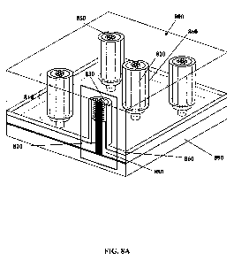
[0100] FIG. 8 shows a nanoscale sensor array 800 according to one embodiment
of
the present invention. The nanoscale sensor array 800 comprises an array of
nanoscale sensor unit structures 810 distributed on a metallized substrate
890. The
array of nanoscale sensor unit structures 810 may be arranged in a uniform,
periodic
or random distribution on the substrate 890. For example, the structures 810
may be
arranged in a hexagonal pattern on the substrate 890. The array of nanoscale
sensor
unit structures 810 may be aligned in rows or unevenly distributed on the
metallized
substrate 890. The metallized substrate 890 may be transparent. The metallized
substrate 890 may be composed of a polymer, glass, ceramic material, carbon
fiber,
glass fiber or combinations thereof onto which a layer of metallic material is
deposited. Those skilled in the art will recognize that the substrate may be
other
materials known in the art and be within the spirit and scope of the presently
disclosed
embodiments.
[0101] An array of vertically aligned conductors 820 (e.g., multiwalled carbon
nanotubes or other types of nanowires or nanofibers) are grown or attached to
the
substrate 890. The conductors 820 are coated with a dielectric material 880.
The
conductors 820 are then coated with a metallic layer 860 acting as the outer
conductor.
-27-
CA 02670073 2009-05-14
WO 2008/133656 PCT/US2007/024043
[0102] The nanoscale sensor apparatus 800 includes vertically aligned carbon
nanotubes 820 grown on a glass substrate coated with a thin (about 10 nm)
chromium
layer. On this layer nickel catalyst for PECVD growth of nanotubes was
deposited
electrochemically. The nanotubes 820 were coated with about 150 nm of aluminum
oxide as the dielectric material 880 and with about 100 nm of chromium as the
metallic layer 860. The entire array of nanoscale sensor unit structures 810
was filled
with spin-on-glass (SOG) which does not affect array functionality but allowed
the
top part of the nanoscale sensor unit structures to be mechanically polished
off. In an
embodiment, the thickness of the SOG is about 6 m. The nanotube 820 in each
sensor unit structure 810 has the same length, unifying the array surface.
Consequently, the capacitance of every nanoscale sensor unit structure 810
will be
close to the same. Nanocavities 830 are formed by chemically etching at least
a
portion of the intermediate dielectric layer 880 between the electrodes 820
and 860.
A nanocavity is opened for every nanoscale sensor unit structure 810. The
nanocavity
830 is adapted to capture target species. Significant impedance change will be
produced corresponding to the molecular accumulation in the nanocavity 830. A
complete nanoscale sensing unit structure 810 is finished upon the addition of
sensing
elements 850 onto nanotubes 820. These sensing elements 850 provide specific
recognition of the target species.
[0103] FIG. 8B shows a sensor device 892 comprising the nanoscale sensor array
800 containing individual unit structures 810. Optionally, the device 892 may
be
integrated with on-chip microfluidics. For example, a microfluidic inlet
channe1894
provides a liquid solution to the array 800. After the solution has been
tested for the
presence of target species by the array 800, the solution is removed through a
microfluidic outlet channel 896. Each unit structure 810 in a given array 800
may test
for the same or different target species. The sensitivity of the device 892 is
amplified
by the number of unit structures 810 in the array 800, which, as shown in the
inset
SEM image in FIG. 8B, can be about 10g/cm2 or less. The volume of solution
provided to the array can be on the order of a few attoliters (1 aL = 10-18 L)
or greater.
[0104] FIG. 9A-9F show a method of making a nanoscale sensor apparatus
according to an embodiment of the present invention. In FIG. 9A, catalyst
particles,
-28-
CA 02670073 2009-05-14
WO 2008/133656 PCT/US2007/024043
such as Ni nanodots, are deposited on a metallized substrate 990. In an
embodiment,
the metallized substrate 990 is a Si wafer coated with a metallic coating such
as
chromium. Carbon deposition is catalyzed underneath the Ni nanodots and forms
a
highly registered nanotube array with the presence of certain gasses, plasma,
and high
temperature (for simplicity, the schematic image shows a single nanotube 920).
Typically, the nanotube 920 diameter is about 50-150 nm.
[0105] FIG. 9B shows a nanoscale coaxial transmission line 900 after the
addition
of a dielectric material 980 and a metallic layer 960 on the nanotube 920. In
an
embodiment, the dielectric materia1980 is alumina and the metallic layer 960
is
chromium. Depending on the size of the target molecule particles for
detection, the
dielectric 980 thickness can be adjusted from tens of nm to hundreds of nm,
such as
about 10 nm to about 500 nm. Both layers are deposited by sputter coating
techniques.
[0106] FIG. 9C shows the nanoscale coaxial transmission line 900 after spin-
coating
of a thick dielectric materia1940. The dielectric materia1940 should be
biocompatible, insulative, stiff, water-resistant, and non-adhesive to
biomolecules. In
an embodiment, the dielectric material 940 is spin-on-glass (SOG).
Alternatively, the
materia1940 is an epoxy, such as "Epon 828".
[0107] FIG. 9D shows the nanoscale coaxial transmission line 900 after
mechanical
polishing the tops of the nanoscale coaxial transmission lines 900 of FIG. 9C.
The
nanotube 920 in each nanoscale coaxial transmission line 900 has substantially
the
same length. Consequently, the capacitance of the nanoscale coaxial
transmission
line 900 will be close to the same.
[0108] FIG. 9E shows the creation of nanocavities 930 in the nanoscale coaxial
transmission lines 900. Nanocavities 930 are created by chemically etching the
intermediate dielectric layer 980 between the nanotube 920 and the outer metal
electrode 960. The nanocavity 930 provides size-dependent physical selection
of
target species entering into the nanocavity. The nanocavity is open at the top
surface
of the coaxial transmission line 900 to allow species having a size greater
than the
opening to enter into the nanocavity and to prevent species having a size
greater than
the opening from entering into the nanocavity. Significant impedance change
will be
-29-
CA 02670073 2009-05-14
WO 2008/133656 PCT/US2007/024043
produced corresponding to the capture of target species in the nanocavity 930.
Partial
etching of the dielectric layer 980 avoids nanotube 920 collapse due to
surface
tension. Preferably, etching is stopped before the nanotube 920 is shorted to
the outer
electrode 960. For example, the length of the nanotube 920 that is not
surrounded by
the dielectric layer 980 is about 50 nm to about 600 nm, such as about 100 nm
to
about 300 nm. In the high magnification SEM image in FIG. 9E, a developed
cavity
structure is broken on purpose to show the internal nanotube 920 component.
[0109] FIG. 9F shows the immobilization of sensing elements (e.g., molecules)
950
onto the top portion of the carbon nanotubes 920. Ferritin proteins were
immobilized
on the CNT by amide linkage, and the crystalline iron cores of the ferritin
proteins are
visible in the TEM image in FIG. 9F. The immobilization can be done by
established
covalent or non-covalent methods. The carbon nanotube 920 can be
functionalized by
chemical groups, or small molecules that carry the reactive groups, such as
carboxylic
acid, amine, and thiol groups. Functionalization can be performed by, for
example,
oxidation using a strong acid, nitrene addition, acrylation using diazonium
salts, and
1,3-dipolar cycloadditions. For example, the carbon nanotube 920 is covalently
functionalized with different types of small molecules to form the following
molecular structures: 1) Ammonium- functionalized CNT; 2) Acetamido-
functionalized CNT; 3) Fluorescein isothiocyanate (FITC)-functionalized CNT;
4)
CNT bifunctionalized with ammonium and FITC; 5) CNT bifunctionalized with
methotrexate (MTX) and FITC; 6)CNT bifunctionalized with amphotericin B (AmB)
and FITC; 7) CNT bifunctionalized with ammonium and FITC. These groups will
render the covalent linkages with the macromolecules. In a non-covalent
version, for
example, the chemical groups carry electro-charges and can facilitate the
electrostatic
attraction of macromolecules on to the nanotube 920 surface. In another
embodiment,
non-covalent immobilization is performed by an electropolymerization process
to coat
the CNTs with conductive (e.g., polypyrrole) and non-conductive (e.g.,
polyphenol)
polymers. The thickness of the polypyrrole coating can be controlled by the
deposition parameters. On the other hand, the polyphenol deposition process
occurs
by a self-limiting process which will stop once a compact and completely
insulative
coating is formed. The polymer coating can be doped with nanostructures (e.g.,
gold
-30-
CA 02670073 2009-05-14
WO 2008/133656 PCT/US2007/024043
nanoparticles) or biomolecules (e.g., glucose oxidase which specifically binds
to
glucose). Another non-covalent strategy is based on the hydrophobic
interaction. The
nanotube 920 surface is originally hydrophobic. It is "sticky" to some
macromolecules
having hydrophobic residues. This mechanism can also be used to functionalize
the
nanotube 920 with small amphiphilic molecules. These molecules can be docked
on
the nanotubes 920 by its hydrophobic part. The hydrophilic end then can
participate in
the direct linkage or interaction with the macromolecules for immobilization.
Many
different CNT chemistries, including covalent and non-covalent chemistries,
can be
used to imrnobilize the active sensing elements on CNTs. For example, the
methods
described by D. Tasis et al., "Chemistry of Carbon Nanotubes," Chem. Rev. 106,
1105-1136 (2006) and K. Kostarelos et al., "Cellular uptake of functionalized
carbon
nanotubes is independent of functional group and cell type," Nature
Nanotechnology
2, 108-113 (2006), all of which are incorporated herein by reference in their
entirety,
can be used.
[0110] A complete nanoscale sensing unit structure 900 will be finished upon
the
addition of active sensing elements 950 onto the top portion of the nanotubes
920.
These active sensing elements 950 provide specific recognition of the sensing
target
species. The specificity is originated from the biological nature of
biomolecule
recognitions, such as antigen-antibody binding, complementary pairing of
nucleotide
molecules, targeted protein binding to certain DNA sequences, and specific
catalytic
activity to the chemical processes of their target molecules, etc. The sensor
900 will
work in a fluidic environment that provides the compatibility to the
biological
activities of the molecules on nanotubes 920 or as the targets dissolved in
the buffer.
[0111] The capture of the targeted species can be transduced to electric
signals by
the sensor 900 through different mechanisms, such as the changes in sensor
impedance, capacitance, and Faradic current, etc. Detection can be performed
by
dielectric spectrometry, capacitance measurement (as of modified from that
combined
with patch clamp technique to measure femto fara level change in membrane
capacitance), time-domain spectroscopy, waveguide resonators at THz
frequencies,
and electrochemical signals from the oxidant or reductant species in the
nanocavity
930. The sensor 900 can detect biological processes occurring within the
nanocavity
-31-
CA 02670073 2009-05-14
WO 2008/133656 PCT/US2007/024043
930, such as molecular redox reactions, enzyme catalyzed reactions, ligand-
receptor
and antigen-antibody interactions, DNA-protein binding and DNA stand
duplexing.
[0112] A method of immobilizing sensing elements onto nanoscale coaxial
transmission lines includes immersing an array of vertically aligned
conductors of
submicron to tens of microns in length supported on a metallized substrate in
oxidative acids at room temperature overnight; rinsing the array with de-
ionized water
followed by critical point drying; sputtering the array with a dielectric
material;
sputtering the dielectric coated array with a metallic material to form
external
conductors; spin coating the array with about 1 to about tens of microns of
insulating
material; polishing the top of the array to expose a top portion of each of
the
conductors; immersing the array in etchant to partially etch off an area of
dielectric
material located at a top portion of the conductors to develop a nanocavity;
immersing
the array in a buffer solution to activate carboxyl groups on the conductors;
adding in
about 1 g macromolecules containing primary amine groups to react with the
functionalized conductors to form amide linkages; and rinsing the array with
de-
ionized water followed by critical point drying. In an embodiment, the array
of
vertically aligned conductors is an array of carbon nanotubes. In an
embodiment, the
oxidative acids may be about 0.5 M nitric acid or a mixture of 3 volume of 98%
sulphric acid and 1 volume of 67% nitric acid. In an embodiment the dielectric
material is sputtered onto the conductors at a thickness of about tens to
about
hundreds of a nanometer. In an embodiment, the metallic material is sputtered
at a
thickness of about 50 to about 200 nm. In an embodiment, the array is immersed
in a
buffer solution of about 0.1 M MES buffer (2-[N-morpholino]ethane sulfonic
acid at
pH 4.5) supplemented with 10 mgl-ethyl-3-(3-dimethylaminopropyl) carbodiimide
(EDC). In an embodiment, the etchant to partially etch off an area of
dielectric
material is a sodium hydroxide solution, for example 100 mM sodium hydroxide
solution.
[0113] An alternative method of immobilizing sensing elements onto nanoscale
coaxial transmission lines includes depositing gold onto an upper portion of
an array
of vertically aligned conductors of submicron to tens of microns in length
supported
on a metallized substrate by e-beam deposition; sputtering the array with a
dielectric
-32-
CA 02670073 2009-05-14
WO 2008/133656 PCT/US2007/024043
material; sputtering the dielectric coated array with a metallic material to
form
external conductors; spin coating the array with about 1 to about tens of
microns of
insulating material; polishing the top of the array to expose a top portion of
each of
the conductors; immersing the array in etchant to partially etch off an area
of
dielectric material located at a top portion of the conductors to develop a
nanocavity;
incubating the array with 1 g thiol modified macromolecules; and rinsing the
array
with de-ionized water followed by critical point drying. In an embodiment, the
array
of vertically aligned conductors is an array of carbon nanotubes. In an
embodiment
the dielectric material is sputtered onto the conductors at a thickness of
about tens to
about hundreds of a nanometer. In an embodiment, the metallic material is
sputtered
at a thickness of about 50 to about 200 nm. In an embodiment, the etchant to
partially
etch off an area of dielectric material is 100 mM sodium hydroxide solution.
In an
embodiment, the array is immersed in about 100 mM sodium hydroxide for about
five
minutes. In an embodiment the array is incubated with thiol modified
macromolecules for about two hours.
[0114] An alternative method of immobilizing sensing elements onto nanoscale
coaxial transmission lines includes immobilizing intermediate macromolecules
with
certain biorecognition properties to the bioreactive macromolecules, which are
in
charge of capturing the target bio-species. In an embodiment, the intermediate
macromolecule is one of DNA probe, PNA (peptide nucleic acid) probe, aptamer,
antibody, avidin, streptavidin, positively charged polymer, and/or negatively
charged
polymer. In an embodiment, the bioreactive macromolecule carries the ligand of
the
intermediate macromolecules, such as DNA, protein, biotin, or certain electric
charge.
[0115] An alternative method of immobilizing sensing elements onto nanoscale
coaxial transmission lines includes depositing gold onto an upper portion of
an array
of vertically aligned conductors supported on a metallized substrate by e-beam
deposition; sputtering the array with a dielectric material; sputtering the
dielectric
coated array with a metallic material to form external conductors; spin
coating the
array with about 1 to about 10 micron of insulating material; polishing the
top of the
array to expose a top portion of each of the conductors; immersing the array
in
sodium hydroxide to partially etch off an area of dielectric material located
at a top
-33-
CA 02670073 2009-05-14
WO 2008/133656 PCT/US2007/024043
portion of the conductors to develop a nanocavity; incubating the array with
streptavidin or thiol modified streptavidin to covalently link the
macromolecules to
the conductors; and rinsing the array with de-ionized water followed by
critical point
drying. In an embodiment, the array of vertically aligned conductors is an
array of
carbon nanotubes. In an embodiment the dielectric material is sputtered onto
the
conductors at a thickness of about tens to about hundreds of a nanometer. In
an
embodiment, the metallic material is sputtered at a thickness of about 50 to
about 200
nm. In an embodiment, the array is immersed in about 100 mM sodium hydroxide
for
about five minutes. In an embodiment the array is incubated with thiol
modified
macromolecules for about two hours.
[0116] An alternative method of immobilizing sensing elements onto nanoscale
coaxial transmission lines includes immersing an array of vertically aligned
conductors supported on a metallized substrate in oxidative acids at room
temperature
overnight; rinsing the array with de-ionized water followed by critical point
drying;
sputtering the array with a dielectric material; sputtering the dielectric
coated array
with a metallic material to form external conductors; spin coating the array
with about
1 to about 10 micron of insulating material; polishing the top of the array to
expose a
top portion of each of the conductors; immersing the array in sodium hydroxide
to
partially etch off an area of dielectric material located at a top portion of
the
conductors to develop a nanocavity; immersing the array in a buffer solution
to
activate carboxyl groups on the conductors; adding in amine enriched polymers
to
conduct aminization between the polymer and the conductors; rinsing the array
with
de-ionized water; transferring the array to neutral sodium chloride solution
with about
1 g macromolecules that carry negative charges at a pH of 7.0; incubating the
array
for about thirty minutes; and rinsing the array with sodium chloride solution
followed
by critical point drying. In an embodiment, the array of vertically aligned
conductors
is an array of carbon nanotubes. In an embodiment, the oxidative acids may be
about
0.5 M nitric acid or a mixture of 3 volume of 98% sulphric acid and 1 volume
of 67%
nitric acid. In an embodiment the dielectric material is sputtered onto the
conductors
at a thickness of about tens to about hundreds of a nanometer. In an
embodiment, the
metallic material is sputtered at a thickness of about 50 to about 200 nm. In
an
-34-
CA 02670073 2009-05-14
WO 2008/133656 PCT/US2007/024043
embodiment, the array is immersed in a buffer solution of about 10 m10.1 M MES
buffer (2-[N-morpholino]ethane sulfonic acid at pH 4.5) supplemented with 10
mgl-
ethyl-3-(3-dimethylaminopropyl) carbodiimide (EDC). In an embodiment the amine
enriched polymer is about 10 l polylysine (0.01 %, 70Kd -140Kd).
[0117] In an embodiment, goat anti-human antibody is inunobilized on a
nanoscale
sensor of the presently disclosed embodiments, which enables the capture of
human
IgG target species in a solution. Impedance Spectroscopy measurements are
performed with a Solartron 1470 Battery Test Unit and a Solartron 1255 B
Frequency
Response Analyzer (Solartron Inc., UK) for 2.5 mM K4[Fe(CN)6] + 2.5mM
K3[Fe(CN)6] in 0.1 M KC1+10 mM PBS (phosphate buffered saline) (pH 7.0)
solution
for the electrochemical detection of human IgG. A sinusoidal potential
modulation of
mV amplitude is superimposed on the formal potential of the redox couple of
[Fe(CN)6]4 -/ [Fe(CN)6]3" (0.22 V vs. Ag/AgCI). The redox couple provides a
background impedance subject to be disturbed by the IgG binding. The change in
the
impedance is calculated and transformed based on the amount of molecular
bindings.
The impedance data may be fitted to the electrical equivalent circuit shown in
FIG.
1B using the Zplot/Zview software (Scribner Associates Inc.). The equivalent
circuit
provides an electrical analogue of chemical/physical processes probed by
Electrochemical Impedance Spectroscopy. Electrolyte solutions are deoxygenated
by
bubbling with high-purity nitrogen for at least 20 min. All measurements are
carried
out at room temperature.
[0118] In order to capture human IgG, the nanoscale sensor is immersed in a pH
7.0
phosphate buffer containing various concentrations of antigen, i.e. human IgG,
at
37 C for 30 min, followed by the rinsing of the nanoscale sensor in 0.01 M PBS
(pH
7.0) solution to remove any unbound antigen. Impedance Spectroscopy
measurements
were then performed, and the results are illustrated by using a Nyquist plot,
of which
each point is the impedance at one frequency. A similar plot is shown in FIG.
10. The
semicircle diameter will increase with the human IgG concentration, signifying
that
more amount of antigen was linked to the interface, and generating a larger
inter-
electrode resistance and stronger blocking to the electron transfer of the
redox probe.
-35-
CA 02670073 2009-05-14
WO 2008/133656 PCT/US2007/024043
[0119] A typical shape of an electrochemical impedance spectrum includes a
semicircle region lying on the Z axis and followed by a straight line. The
semicircle
portion, observed at higher frequencies, corresponds to the electron-transfer
limited
process, whereas the linear part is characteristic of the lower frequencies
range and
represents the diffusional limited electron-transfer process. In the case of a
very fast
electron-transfer process, the impedance spectrum could include only the
linear part,
whereas a very slow electron-transfer step results in a big semicircle region
that is not
accompanied by a straight line. The electron-transfer kinetics and diffusional
characteristics can be extracted from the spectra.
[0120] As stated above, the equivalent circuit of FIG. 10 suggests the
approach for
detecting target species is Impedance Spectroscopy or Dielectric Spectroscopy.
There
are a number of different dielectric mechanisms, connected to the way a
studied
medium reacts to the applied field, as shown in FIG. 11. Each dielectric
mechanism is
centered around its characteristic frequency, which is the reciprocal of the
characteristic time of the process. In general, dielectric mechanisms can be
divided
into relaxation and resonance processes. The most common, starting from high
frequencies, are 1) Electronic polarization, this resonant process occurs in a
neutral
atom when the electric field displaces the electron density relative to the
nucleus it
surrounds; 2) Atomic polarization is observed when an agglomeration of
positive and
negative ions is deformed under the force of the applied field. This is also a
resonant
process; 3) Dipole relaxation, which originates from permanent and induced
dipoles
aligning to an electric field. Their orientation polarization is disturbed by
thermal
noise (which dis-aligns the dipole vectors from the direction of the field),
and the time
needed for dipoles to relax is determined by the local viscosity. These two
facts make
dipole relaxation dependant on temperature and chemical surrounding; and 4)
Ionic
relaxation, which is comprised of ionic conductivity and interfacial and space
charge
relaxation. Ionic conductivity predominates at low frequencies and introduces
only
losses to the system. Interfacial relaxation occurs when charge carriers
become
trapped at interfaces of heterogeneous systems.
[0121] Dielectric Spectroscopy has been used in materials science, and also in
studying the electrical properties of biological materials. Impedance
Spectroscopy is
-36-
CA 02670073 2009-05-14
WO 2008/133656 PCT/US2007/024043
gaining renewed strength as a tool complementary to other techniques used to
study
the structural and related properties of proteins by providing important
information
about the protein's charge dynamics, as related to its structure. Impedance
Spectroscopy is sensitive to polarization interfaces and intermolecular
interactions,
such as dipole-dipole interactions and cooperative processes.
[0122] FIG. 12 shows an experimental setup for Impedance Spectroscopy. For
example, a Solartron 1260 impedance/gain-phase analyzer is used to sweep the
frequency over a range of about 1 Hz to about 1 MHz. The liquid cell with
stainless
steel electrodes was 2 cm in diameter, and contained a guard ring that reduced
fringing fields. The separation distance used in the experiments between the
electrodes was 1 mm.
[0123] AE = (Es,- C.) = g, 2NAC (3)
2EoMkT
[0124] Equation (3) tells us that, by measuring the low- and high-frequency-
limiting
dielectric constants, ES and E., one can calculate the dipole moment of the
protein for
given assumptions of g, thereby, to determine its identity based on the
fingerprint.
This relationship has been used for extracting with high accuracy the
electrical dipole
moment for other biomolecules, such as myoglobin, hemoglobin, DNA, etc. is
the
dipole moment of the protein, NA is Avogadro's number, C is the concentration
in
(mg/ml), M is the mass of the protein (kg/mol), k is the Boltzmann constant, T
the
absolute temperature, and g is the Kirkwood correlation factor, which is
usually
assumed to be 1.
[0125] Time Domain Dielectric Spectroscopy (TDDS) is based on the transmission
line theory in the time domain and studies the heterogeneity in the coaxial
lines
according to the change in shape of a test signal. In this method a rapidly
increasing
voltage step arrives at the sampling head where the signal reflected from the
dielectric
sample is also registered. For the ideal system, the voltage applied to the
sample is:
[0126] V (t) = Vo (t) + V, (t)
-37-
CA 02670073 2009-05-14
WO 2008/133656 PCT/US2007/024043
[0127] where Vo (t) and Vr (t) are the incident and reflected signals,
respectively.
The expression for the flow of current through the sample is
[0128] 1(t) = ~ [Vo (t) - R(t)j
0
[0129] where Zo is the characteristic impedance of the transmission line in
the
absence of a target specie between the conductors.
[0130] As long as the transmission line is homogeneous, the shape of this
pulse will
not change. But, in the case of heterogeneity in the line (for example, when a
target
specie is present between the conductors) the signal is partly reflected from
the air-
dielectric interface and partly passes through it. Dielectric measurements are
made
along a coaxial transmission line with the sample mounted in a sample cell
that
terminates the line.
[0131] FIG 12 illustrates the experimental set-up used for the TDDS method
according to an embodiment of the present invention. The recorded signals are
shown
in FIGS. 13 and 14.
[0132] FIG. 13 is an illustration of the basic principles of the TDDS system,
where
Vo(t) is the incident pulse and R(t) is the reflected signal.
[0133] FIG. 14 shows the characteristic shape of the signals recorded during a
TDDS experiment.
[0134] The low-frequency conductivity (a) of the sample can be determined
directly
in time domain. Here, Eo = 8.85 x 10⁻¹² F/m, and Co is the electric capacity
of the
coaxial sample cell terminated to the coaxial line.
[0135] a = s lim
Z Co - V (t) + R(t)
[0136] FIG. 15A-15D are SEM images showing the steps used to fabricate an
ordered pattern of nanocoaxial sensors according to an embodiment of the
present
invention. FIG. 15A shows a self-assembled mask of polystyrene nanospheres
deposited on a substrate. E-beam deposition was used to deposit Ni catalyst in
the
interstices of the nanosphere mask. FIG. 15B shows the Ni catalyst after it
was
-38-
CA 02670073 2009-05-14
WO 2008/133656 PCT/US2007/024043
annealed to form a hexagonal pattern of Ni nanodots on the substrate surface.
FIG.
15C shows the surface after CVD was performed to grow vertically-aligned CNTs
at
the catalyst, sites. FIG. 15D shows an array of completed nanocoaxial sensors
after
the dielectric and outer conductors were deposited onto the CNTs. The distance
between each nanocoaxial sensor can be adjusted by varying the size of the
nanospheres. Other types of masks having different patterns can also be used.
The
spatial amplification of the nanosensor array can be adapted to scale linearly
with the
number of nanosensors in the array. For example, the array is group
addressable. In
an embodiment, the individual nanocoaxial sensors in an array are connected in
parallel and the total capacitance of the array is the sum of the capacitance
of each
individual nanocoaxial sensor. In another embodiment, the individual
nanocoaxial
sensors in an array are connected in series and the total capacitance of the
array is the
inverse of the sum of the inverse capacitance of each individual nanocoaxial
sensor.
[0137] FIG. 16A-16D show the precise placement and spatial arrangement of an
ordered arrangement of CNTs formed on tungsten leads. FIG. 16A and 16B are SEM
images of tungsten leads formed on a Si substrate. The tips of the tungsten
leads are
spaced apart from each other, with gaps ranging from about 40 nm to about 1
m. A
single Ni catalyst nanodot having a diameter of about 100 nm is deposited on
the tip
of each lead, as shown in FIG. 16B. FIG. 16C shows an AFM image of the same
leads. FIG. 16D is a SEM image of the leads after CNTs are grown from the Ni
catalyst nanodots. Nanocoaxial sensors are formed around each CNT by
depositing a
dielectric and an outer metal layer around each CNT. Each nanocoaxial sensor
in the
array can operate independently of the others in the array. For example, the
inner
conductor of each sensor is not in electrical contact with any other inner
conductor in
the array, allowing each inner conductor to be probed at a different bias. The
independently addressable array of nanocoaxial sensors allows multiplexing of
the
signal being provided by each sensor.
[0138] FIG. 17 shows four SEM images of nanocoaxial sensors having different
sized nanocavity openings according to an embodiment of the present invention.
The
distance between the inner conductor and the outer conductor can be tuned by
changing diameter of the inner conductor or the thickness of the dielectric
material, or
-39-
CA 02670073 2009-05-14
WO 2008/133656 PCT/US2007/024043
both. For example, when a CNT is used as the inner conductor, the diameter of
the
CNT can be controlled by the size of the catalytic Ni particle used. Also, the
thickness of the dielectric material is controlled by the duration of the
magnetron
sputtering deposition. The depth of the nanocavity can be tuned by etching the
dielectric material with different etchants or by varying the duration of the
etching
step, or both. The CNT diameter can be adjusted from about 40 nm to about 200
nm.
The thickness of the dielectric can be adjusted from about 10 nm to about 500
nm.
The depth of the nanocavity can be adjusted from about 50 nm to about 2000 nm.
The nanocavity is adapted to exhibit a size-dependent physical selection of
target
species entering into the nanocavity. The size of the nanocavity opening is
adjusted
depending on the size of the target species to be detected by the nanocoaxial
sensor.
For example, a size of the nanocavity opening is selected such that
substantially no
molecules having a size greater than a critical size will enter into the
nanocavity. The
critical size is determined for a given target species, for example, by
applying
differently-sized target species, such as E. coli (ranging 0.5X1.5 m to
0.8x2.2 m) or
SARS-CoV (ranging diameter 60 nm to 120 nm), to an array of nanocoaxial
sensors
of known opening size.
[0139] The nanocavities of the present invention are compatible with various
methods for filling the nanocavities with solution. For example, the
nanocavities are
filled with solution by capillary action, whereby the nanocavity surface
(e.g., the walls
of the outer and/or inner conductors within the nanocavity) effectively draw
the
solution into the nanocavity by hydrophobic/hydrophilic interactions. Capillay
action
is optimized by judicious choice of conductor materials and carrier solvent.
In
addition, the solution can be drawn into the nanocavity by an electrowetting
process,
whereby an electrical potential is applied to the inner and/or outer
conductors. For
example, the electrowetting method described in an article by J. Y. Chen et
al.,
"Electrowetting in Carbon Nanotubes," Science 310, 1480-1483 (2005), which is
incorporated herein by reference in its entirety, can be used. Optionally, a
supercritical filling process can be performed, including first filling the
nanocavity
with liquid carbon dioxide and then filling the nanocavity with the solution
by
substitution. For example, the supercritical filling process described in the
article by
-40-
CA 02670073 2009-05-14
WO 2008/133656 PCT/US2007/024043
X. B. Wang et al., "Nanofluids in carbon nanotubes using supercritical CO 2: a
first
step towards a nanochemical reaction," Applied Physics A 80, 637-639 (2005),
which
is incorporated herein by reference in its entirety, can be used. The target
species can
be labeled with magnetic and/or electrically charged nanoparticles and drawn
into the
nanocavities by magnetic and/or electrostatic attraction to complementary
nanoparticles that are immobilized within the nanocavities. In an embodiment,
the
target species are magnetically and/or electrostatically drawn to the target
species.
Optionally, if CNTs are used as the inner conductors, an electrical potential
is applied
to the CNTs to enhance the electrostatic attraction.
[0140] FIG. 18 shows nucleation of a gold film and CNT functionalization
according to an embodiment of the present invention. FIG. 18A shows the
experimental setup in which a gold film deposited on a quartz substrate was
heated at
a temperature (T) while its resistivity (mSl-cm) was measured. FIG. 18B shows
that
the resistivity of the gold film increased exponentially as the temperature
was
increased from 270 C to 450 C, above which the resistivity became to large to
be
measured, thus indicating the loss of electrical connection between the two
electrodes.
The inset of FIG. 18B shows SEM images of the gold film before (right) and
after
(left) the thermal anneal. As can be seen, the gold film nucleated into
discreet and
electrically isolated gold nanoparticles.
[0141] FIG. 18C shows a method of functionalizing CNTs with gold
nanoparticles.
First, CNTs are grown by CVD or other suitable method on patterned electrodes,
such
as on the tungsten leads shown in FIG. 16A-16D. Second, the CNTs are coated
with
a gold film having a thickness of about 1 nm to about 12 nm by thermal or
electron
beam evaporation. Third, the gold film is annealed at a temperature greater
than
about 450 C, such as about 500 C to about 650 C for 45 min in a horizontal
tube
furnace with constant flowing Ar gas (50 sccm) and pressure of 5 Torr. The
gold film
is broken into discrete nanoparticles, and the CNTs grown on different
electrodes are
not in electrical contact with each other. Fourth, the gold-functionalized
CNTs are
coated with a dielectric material and then coated with an outer metal layer.
At least a
portion of the dielectric material is etched away to form a nanocavity and to
reveal the
gold nanoparticle-functionalized CNT. These gold nanoparticles are available
for
-41-
CA 02670073 2009-05-14
WO 2008/133656 PCT/US2007/024043
subsequent chemistries. For example, an anti-Fc-y antibody is modified with a
thiol
group through a C7 crank and is then bound to the gold nanoparticle-
functionalized
CNT. A secondary antibody (anti-SARS mAb) is then bound to the anti- Fcy
antibody for selective capture of SARS-CoV virus.
[0142] The foregoing description of the invention has been presented for
purposes
of illustration and description. It is not intended to be exhaustive or to
limit the
invention to the precise form disclosed, and modifications and variations are
possible
in light of the above teachings or may be acquired from practice of the
invention. The
description was chosen in order to explain the principles of the invention and
its
practical application. It is intended that the scope of the invention be
defined by the
claims appended hereto, and their equivalents.
-42-