Note: Descriptions are shown in the official language in which they were submitted.
CA 02670180 2009-06-22
MBM File No. 1308-110
SYSTEM, DEVICE AND METHOD FOR HIGH DYNAMIC
RANGE DIGITAL IMAGING
FIELD OF THE INVENTION
[0001) The present invention pertains to the field of digital imaging, and in
particular, to pixels
for digital imaging systems capable of providing large amplification, high
dynamic range and
fast pixel readout time.
BACKGROUND
100021 Active matrix flat-panel imagers (AMFPIs) have gained considerable
significance in
digital imaging, and specifically in diagnostic medical imaging applications,
in view of their
large area readout capability. An AMPFI comprises a matrix of pixels, each
forming a
fundamental unit of the active matrix. Each pixel comprises a detector and
readout circuitry for
transfer of collected electrons to external electronics for data acquisition.
The pixel most
commonly used for large area X-ray imaging is the passive pixel sensor (PPS)
100 shown in
Figure IA. The PPS comprises a detector 101, for example, an amorphous
selenium (a-Se) based
photoconductor or a Caesium Iodide (CsI) phosphor coupled to an amorphous
silicon (a-Si:H)
PIN photodiode, or an adequate metal insulator diode that is integrated with a
readout circuit
comprising an a-Si:H thin-film transistor (TFT) switch. Charges generated by
photons are
accumulated on the pixel capacitance during an integration cycle and is
transferred to an external
charge amplifier via the TFT switch during a readout/reset cycle. The
capacitance may arise
from the PIN photodiode capacitance or an integrated storage capacitor for the
a-Se
photoconductor arrangement, for example. Figure 1 B illustrates a timing
diagram for a sequence
of operations of a PPS. Cycle 110 and 120 represent the integration cycle and
readout/reset
cycle, respectively. Other sequences are possible, for example, where double
sampling
mechanisms are introduced, wherein double sampling mechanisms are typically
used to correct
for the effect of non-uniformities within the circuitry. These non-
uniformities may comprise
process non-uniformities in the form of offsets, and, in the case of a-Si:H
technology, non-
uniformities in pixel circuit performance due to transistor instability. For
example, International
2
CA 02670180 2009-06-22
MBMFile No. 1308-110
Patent Application Publication Nos. WO 96/34416 and WO 97/05659 disclose flat-
panel
detectors for radiation imaging using a PPS.
[00031 While the PPS has the advantage of being compact and thus amenable to
high-
resolution imaging, reading a small output signal of the PPS for low input,
real-time, large area
applications, such as low dose fluoroscopy, requires high performance off-
panel column charge
amplifiers. These charge amplifiers can add noise and degrade the signal-to-
noise ratio (SNR) at
low signal levels and reduce the useful dynamic range of the pixel. In
particular, fluoroscopy can
be one of the most demanding applications for flat-panel imaging systems due
to the requirement
of real-time readout. Real-time X-ray imaging or fluoroscopy is used in many
medical
interventional procedures where a catheter is moved through the arterial
system under X-ray
guidance. The technical challenge to be addressed for these types of
fluoroscopy is the need for
extremely low noise, or alternatively, an increase in signal size before
readout. Studies on a-Si:H
PPS suggest that an improvement in SNR of an order of magnitude is desirable
in order to apply
these systems to more advanced imaging applications.
[0004] One approach for improved SNR is disclosed in International Patent
Application
Publication No. WO 02/067337 which discloses that the SNR can be increased by
employing in-
situ, per-pixel amplification via an a-Si:H current-mediated active pixel
sensor (C-APS) 200 as
illustrated in Figure 2A. The gain, linearity and noise results reported show
an improvement and
indicate that the a-Si:H C-APS, coupled together with an established X-ray
detection technology
such as a-Se or CsI/PIN photodiodes, can meet the stringent noise requirements
for digital X-ray
fluoroscopy. Noise may be required to be less than 103 electrons.
[0005] To perform amplification of input signals of small magnitude that are
vulnerable to
noise, such as in fluoroscopy, the C-APS pixel can be used in three operating
cycles; a reset
cycle, an integration cycle and a readout cycle. Figure 2B illustrates a
timing diagram for a
method of operating the C-APS readout circuit employing a double sampling
mechanism. During
an integration cycle 210, READ transistor 24 and RESET transistor 21 are kept
OFF while
AMP_RESET transistor 27 is kept ON. Photons incident upon detector 22 result
in the
generation of electron-hole pairs that can discharge or charge the capacitance
CDETECTOR at node
201 and thus can reduce or increase the voltage at node 201, VG, by an amount
AVG.
3
CA 02670180 2009-06-22
MBMFile No. 1308-110
[0006] The readout cycle 220 follows the integration cycle 210 and during this
cycle, READ
transistor 24 is turned ON, RESET transistor 21 is kept OFF and the AMP_RESET
transistor 27
is turned OFF, resulting in a current, Ibias Dlbias, that is proportional to
VG AVG flowing in the
AMP transistor 23 and READ transistor 24 branch. The current, Ibias Dlbias
is then integrated by
charge amplifier 25 to obtain and store an output voltage, VovTi, on the
amplifier feedback
capacitor 26.
[0007] The reset cycle 230 occurs subsequent to the readout cycle 220 where
RESET transistor
21 is pulsed ON and CDETECTOR is charged, or discharged, to reset the voltage
at node 201 to VG
while RESET transistor 21 is ON. During this reset cycle, READ transistor 24
is turned OFF and
AMP RESET transistor 27 is turned ON.
[0008] To perform the double sampling operation, an additional read cycle 240
follows the
reset cycle 230 where again READ transistor 24 is turned ON, RESET transistor
21 is turned
OFF and AMP_RESET transistor 27 is turned OFF. Ibias is integrated by charge
amplifier 25 to
obtain and store an output voltage, VoUu, on feedback capacitor 26.
Subtracting VOUTI from
VoUT2 yields a OVoUT that can be free from non-uniformities and is
proportional to AVG. AIbias is
proportional to AVG and is given as:
Dlbias = gmAVG,
[0009] where gm is the transconductance of the AMP transistor 23 and READ
transistor 24
readout circuit branch.
[0010] The C-APS produces a charge gain, Gi, to amplify the noise vulnerable
input signal.
The Gi for the C-APS is given as:
Gi = (gmTSYCDETECTOR,
[0011] where Ts is the amount of time Ibias and AIbias are integrated on the
feedback capacitor
26. As indicated by the equation above, Gi is programmable via g,,,, Ts and
the choice of an
appropriate CDETECTOR.
4
CA 02670180 2009-06-22
MBMFile No. 1308-110
[0012] A concern with the C-APS circuit is the small-signal linearity on the X-
ray input signal.
Using such a pixel sensor, for example in real-time fluoroscopy applications,
where the radiation
intensity levels are small, is feasible since the voltage change at the
amplifier input is also small
and in the order of mV. In applications that require higher radiation
intensity, however, for
example in digital chest radiography, mammography or higher dose fluoroscopy,
the voltage
change at the amplifier input can be much larger due to the larger X-ray
exposure levels, which
can cause the C-APS pixel sensor output to be non-linear thus reducing the
dynamic range of the
pixel sensor. Another consequence of a non-linear transfer function of the
amplifier is that, for
example a double sampling mechanism, can not effectively be implemented in
hardware due to
this non-linearity.
[0013] One solution to the problem of low dynamic range is to employ a multi-
mode pixel
sensor (MMPS) as disclosed in International Patent Application Publication
No. WO 2005/015639. In the MMPS the readout circuitry functions in different
modes which
may be selected depending on the characteristics of the input signal
transferred to the readout
circuitry from the detector. For example, when the input signal has a
particular magnitude or
range of magnitudes the readout circuitry can function in a first mode wherein
the input signal
can be amplified, and when the input signal has a different magnitude or range
of magnitudes the
readout circuitry can function in an alternate mode wherein the signal can be
read out with a
different or no amplification.
[0014] Another shortcoming of the C-APS pixel is that the presence of a large
output current
can cause saturation of the external or off-panel charge amplifier. Large
pixel output currents can
also occur when a large charge gain is required since g,, is proportional to
Ib;as. International
Patent Application Publication No. WO 2005/015639 discloses the use of a
current subtraction
circuit to deal with saturation of the amplifier. Current subtraction may
require additional
circuitry for dealing with offsets between pixels and can add cost to the
system and introduce
undesired noise to the output signal.
[0015] Another approach disclosed in International Patent Application
Publication
No. WO 02/067337 teaches a near-unity gain pixel amplifier, for example, an a-
Si:H voltage-
mediated active pixel sensor (V-APS). A general V-APS schematic is illustrated
in Figure 3.
MBMFile No. 1308-110 CA 02670180 2009-06-22
Detector 32, READ transistor 34, AMP transistor 33 and RESET transistor 31 are
components of
the V-APS pixel and function in a similar manner as in the C-APS pixel.
Resistive load 35 is
connected to the pixel output node to convert the current in the AMP
transistor 33 and READ
transistor 34 branch into an output voltage. Resistive load 35 can comprise a
resistor load device
or a transistor load device. The input signal voltage VG is translated to a
pixel output voltage
VOUT with a near unity gain. The V-APS, like the C-APS, can be used in three
operating cycles; a
reset cycle, an integration cycle and a readout cycle. Like the C-APS, double
sampling
mechanisms can be applied to the V-APS to correct for the effect of non-
uniformities within the
circuitry. A problem with the V-APS is that essentially no gain is provided to
the input signal. In
addition, with current state of the art amorphous silicon technology, it is
difficult to achieve real
time readout using this pixel when large column bus capacitances are charged
and discharged.
[0016] U.S. Patent Application Publication Nos. 2007/0187609 and 2008/0259182
describes
pixels for multi-mode readout to extend the prior art described above. Here,
the pixel readout is
separated into multiple modes: unity gain (PPS mode and V-APS) and high gain
(C-APS mode).
In the unity gain mode the readout speed of the pixel, however, is limited by
either the RC time
constant of the pixel capacitance and readout transistor for the PPS or the RC
time constant of
the column line capacitance and the readout transistor for the V-APS. The
readout for the PPS
and V-APS imposes a limit on the overall readout speed of the pixel in multi-
mode operation.
[0017] Therefore, there is a need for pixels that may overcome at least one of
the deficiencies
known in the art.
[0018] This background information is provided for the purpose of making known
information
believed by the applicant to be of possible relevance to the present
invention. No admission is
necessarily intended, nor should be construed, that any of the preceding
information constitutes
prior art against the present invention.
SUMMARY OF THE INVENTION
[0019] An object of the invention is to provide a system, device and method
for high dynamic
range digital imaging. In accordance with an aspect of the invention, there is
provided a
detecting system for an imaging device, the detecting system comprising: a
detector for
6
MBMFile No. 1308-110 CA 02670180 2009-06-22
converting electromagnetic radiation to electrical charge; and a capacitor
system operatively
connected to the detector, the capacitor system configured to be switchable
between a first
capacitance and a second capacitance, thereby providing the detecting system
with a controllable
capacitance for storing the electrical charge.
[0020] In accordance with another aspect of the invention, there is provided
an imaging device
comprising: a detecting system including: a detector for converting
electromagnetic radiation to
electrical charge; and a capacitor system operatively connected to the
detector, the capacitor
system switchable between a first capacitance and a second capacitance,
thereby providing the
detecting system with a controllable capacitance for storing the electrical
charge; and readout
circuitry operatively coupled to the detecting system, the readout circuitry
configured to
determine the stored electrical charge and provide an output signal indicative
of the stored
electrical charge.
[0021] In accordance with another aspect of the invention, there is provided
an imaging system
comprising: a plurality of imaging devices, each imaging device comprising: a
detecting system
including a detector for converting electromagnetic radiation to electrical
charge and a capacitor
system operatively connected to the detector, the capacitor system switchable
between a first
capacitance and a second capacitance, thereby providing the detecting system
with a controllable
capacitance for storing the electrical charge; and readout circuitry
operatively coupled to the
detecting system, the readout circuitry configured to determine the stored
electrical charge and
provide an output signal indicative of the stored electrical charge; and a
control system
operatively coupled to the plurality of imaging devices for collecting the
plurality of output
signals received from the plurality of imaging devices.
[0022] In accordance with another aspect of the invention, there is provided a
method for
operating a detecting system for an imaging device, the detecting system
comprising a detector
operatively coupled to a capacitor system switchable between a first
capacitance and a second
capacitance, the method comprising: determining a desired capacitance of the
capacitor system;
configuring the capacitor system with the desired capacitance; converting
electromagnetic
radiation into electrical charge carriers by the detector; storing at least a
portion of the charge
carriers as charge in the capacitor system; and determining the charge.
7
CA 02670180 2009-06-22
MBMFile No. 1308-110
BRIEF DESCRIPTION OF THE FIGURES
[0023] Figure lA illustrates a schematic of a passive pixel sensor.
[0024] Figure 1 B illustrates a timing diagram for a method of operation of
the pixel sensor of
Figure 1 A.
[0025] Figure 2A illustrates a schematic of a current-mediated active pixel
sensor.
100261 Figure 2B illustrates a timing diagram for a method of operation of the
pixel sensor of
Figure 2A.
100271 Figure 3 illustrates a schematic of a voltage-mediated active pixel
sensor.
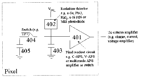
[0028] Figure 4 illustrates a schematic of a pixel sensor according to
embodiments of the
invention.
[0029] Figure 5 illustrates a schematic of another pixel sensor according to
embodiments of the
invention.
DETAILED DESCRIPTION OF THE INVENTION
Definitions
[00301 The term "detector" is used to 'refer to a device that can convert
electromagnetic
radiation within a predetermined wavelength range into electrical charge. The
predetermined
wavelength range may include one or more portions of the electromagnetic
spectrum, for
example, X-ray, ultraviolet, infrared, or other electromagnetic radiation
range or combination of
ranges or portions thereof, as would be readily understood. The term
"electromagnetic radiation"
may be used herein synonymously with the term "photon" as the case may be.
[0031] The term "sensor" is used to define the combination of one or more
detectors and
circuitry that may be used for determining all or a portion of the electrical
charge of a detector.
[0032] The term "unity gain" is used to define a signal amplification, for
example a current or
voltage gain, wherein the order of magnitude of the output signal obtained as
a result of the gain
8
CA 02670180 2009-06-22
MBMFile No. 1308-110
being applied to an input signal substantially corresponds with the order of
magnitude of the
input signal.
[0033] Unless defined otherwise, all technical and scientific terms used
herein have the same
meaning as commonly understood by one of ordinary skill in the art to which
this invention
belongs.
[0034] The invention provides a detecting system which is configured to
selectively
adjustment the capacitance associated therewith. The detecting system
comprises a detector for
converting electromagnetic radiation into an electrical charge, wherein the
detector is operatively
coupled to a capacitive system configured to selectively switch between a
first detecting system
capacitance and a second detecting system capacitance. This selective
adjustment of the
capacitance of the detecting system is based at least in part on the radiation
intensity impinging
on the detector. Further provided is an imaging device which comprises a
detecting system and
readout circuitry operatively coupled to the detecting system, wherein the
readout circuitry
provides a means for sampling a signal indicative of the radiation impinging
on the detector. As
used herein, an imaging device may also be referred to as a "pixel". Further
provided is an
imaging system according to embodiments of the invention, which comprises a
plurality of
imaging devices, each of which includes a detecting system and readout
circuitry.
[0035] Each detector generates charge carriers, for example electrons and/or
holes, in response
to photons that are adequately absorbed by the detector. Absorbed photons can
result in a voltage
change across the detector. This voltage change produces the input signal to
the readout circuitry.
According to embodiments of the invention, the readout circuit is configured
to provide electrical
current or charge representative of the input signal.
[0036] According to some embodiments of the invention, the readout circuitry
achieves high
dynamic range and high gain while operating in one of one or more readout
modes, for example
in C-APS or V-APS. According to embodiments of the invention, this may be
achieved by
varying the capacitance of the pixel used to hold the charge generated by
absorbed photons. A
pixel according to embodiments of the invention may optionally be configured
to provide more
than one readout mode.
9
CA 02670180 2009-06-22
MBMFile No. 1308-110
Detecting System
[0037] The detecting system comprises a detector for converting
electromagnetic radiation into
an electrical charge. The detector is operatively coupled to a capacitive
system configured to
selectively switch between a first detecting system capacitance and a second
detecting system
capacitance. This selective adjustment of the capacitance of the detecting
system is based at
least in part on the radiation intensity impinging on the detector. According
to embodiments of
the invention, one or more of a third detecting system capacitance, fourth
detecting system
capacitance etc. may also be provided by the detecting system.
[0038] Figure 4 illustrates a schematic of a detecting system according to
embodiments of the
invention. The detecting system comprises a readout circuit 401, a detector
402, a pixel capacitor
403, a pixel switch 404 and an additional pixel capacitor 405. The combination
of pixel switch
404 and additional pixel capacitor 405 allows for selection of the pixel
capacitance from a
plurality of predetermined capacities in correspondence with radiation
intensity requirements of
the application.
[0039] According to some embodiments of the invention a detecting system may
comprise one
or more switches and capacitors operatively interconnected to form one of one
or more
predetermined network configurations by selectively opening and/or closing
predetermined
switches. According to embodiments of the invention a detecting system may be
configured to
operate linearly within one or more ranges of predetermined operating
conditions. For example,
for low signal (i.e. small input charge), pixel capacitor 403 may be
dimensioned to yield a first
predetermined voltage to get a linear response from readout circuit 401; and
for high signal (i.e.
large input charge), pixel capacitor 405 can be connected in parallel to pixel
capacitor 403 via
switch 404 to increase the pixel capacitance in order to provide a
predetermined voltage for a
linear response from 401.
[0040] A detecting system according to embodiments of the invention may
comprise a serially
connected, non-biased detector and a pixel capacitor, and one switch for
selectively shorting the
pixel capacitor. The one switch may be used to operatively activate the one
pixel capacitor in
parallel to the intrinsic capacitance of the detector in order to add the
capacitance of the pixel
capacitor to the intrinsic capacitance when the switch is closed. It is noted
that one detector, one
CA 02670180 2009-06-22
MBMFile No. 1308-110
pixel capacitor and one switch may be interconnected in other ways to provide
and controllable
capacitance.
[0041] The detector may comprise an amorphous selenium (a-Se) based
photoconductor or a
Caesium Iodide (CsI) phosphor coupled to an amorphous silicon (a-Si:H) PIN
photodiode, or an
adequate metal insulator diode that is integrated with a readout circuit
comprising an a-Si:H thin-
film transistor (TFT) switch, for example. The detector may be any type of
detector, for example,
solid-state photodetectors such as a-Si:H, amorphous selenium, lead iodide,
mercuric iodide, lead
oxide or cadmium zinc telluride based detectors or other appropriate detector.
In addition, direct
detection based detectors such as molybdenum Schottky diodes, as well as
detectors based on
indirect detection such as those comprising phosphors, for example gadolinium
oxysulfide
detectors or caesium iodide detectors, may also be used. A photodiodes may be
configured and
employed in a detecting system to provide a combination of detector and pixel
capacitor.
[0042] The one or more pixel capacitors may comprise metallic layers separated
by one or
more layers of one or more adequate dielectric materials. A switch may
comprise an adequately
configured transistor, for example, a field effect transistor. Components of
the detecting system
including detectors, capacitors and/or switches, may be disposed using thin-
film technology,
epitaxially or in another manner as would be readily understood. For example,
a switch may be a
transistor configured as a n-type, p-type or ambi-polar transistor. Components
of the detecting
system may be at least partially integrally formed, for example, the detector
and one or more of
the capacitors may share a one or more common layers of one or more materials.
Interconnections between components of the detecting may be formed from/by
common
elements of components and/or traces of adequately conductive material. Like
aspects may apply
to readout circuitry and imaging systems.
[0043] A capacitor system according to embodiments of the invention may
comprise two or
more capacitors and one or more switches for operatively interconnecting the
capacitors in a
number of predetermined configurations, for example, in a purely parallel or
serial, or in a mixed
parallel-serial configuration. The capacitor system may be configured to
permit reconfiguration
of the interconnection of the capacitors during operation.
11
CA 02670180 2009-06-22
MBMFile No. 1308-110
[0044] According to embodiments, the detecting system comprises a reset
switch, for example
a transistor, for operatively connecting the capacitor system to a
predetermined potential for
disposing a predetermined charge in the capacitor system when closing the
reset switch.
Readout Circuitry
[0045] A readout circuitry according to some embodiments of the invention may
be configured
to provide large amplification to small, noise sensitive input signals,
improved noise immunity,
and/or fast pixel readout time, for example. A pixel according to some
embodiments of the
invention may be able to provide high speed readout irrespective of whether
the pixel operates in
unity or high gain mode and/or be able to achieve real-time readout as well as
achieve high gain
to detect small noise-vulnerable signals with a large signal-to-noise ratio
while being capable of
sensing a wide range of input signals.
[0046] According to some embodiments of the invention, a readout circuit may
be
preconfigured to operate in one predetermined mode, for example in a voltage-
or current-
mediated active pixel sensor mode, or in one out of two or more predetermined
modes which can
be selected during operation. For example, in a multi-mode imaging device or
multi-mode
imaging devices of an imaging system, the readout circuitry may be configured
to operate in one
of a plurality of modes which may be selected depending on the characteristics
of the input
signal provided to the readout circuitry from the detector. For example, when
the input signal has
a particular magnitude or range of magnitudes the readout circuitry can
function in a first mode
wherein the input signal can be amplified, and when the input signal has a
different magnitude or
range of magnitudes the readout circuitry can function in an alternate mode
wherein the signal
can be read out with a different or no amplification, for example, as is
described in International
Patent Application Publication No. W02005/015639.
[0047] A readout circuitry according to embodiments of the invention comprises
an on-pixel
amplifier, for example a transistor, and additional transistors for reading
out the amplified signal
and/or to reset the amplified output signal stored by a portion of the circuit
prior to reading a
subsequent signal. Transistors for reading and resetting may be disposed in
various parts of the
readout circuitry. One of more transistors and/or additional components, for
example resistors,
inductors or capacitors, may also be used in addition to the amplification
transistor for
12
CA 02670180 2009-06-22
MBM File No. 1308-110
amplification. Power sources and components such as resistors, inductors and
capacitors, in
addition to the amplification, read and reset transistors may also be
implemented in the readout
circuitry.
[0048] The readout circuitry is configured to provide a signal representative
of the voltage or
charge generated by the one or more detectors in response to adequately
absorbed photons.
According to embodiments of the invention, the readout circuitry may be
configured to provide
large amplification of small, noise sensitive input signals to improve their
noise immunity, as
well as capable of providing a fast pixel readout time. The readout circuitry
may comprise an on-
pixel amplification transistor as well as additional transistors used to read
out the amplified
signal and/or to reset the amplified output signal stored by a portion of the
circuit prior to reading
a subsequent signal, wherein the read transistors and reset transistors are
able to occupy various
positions within the readout circuitry. More than one transistor as well as
additional components,
such as resistors, inductors and capacitors, may also be used in addition to
the amplification
transistor for amplification. Power sources and components such as resistors,
inductors and
capacitors, in addition to the amplification, read and reset transistors may
also be implemented in
the readout circuitry. For example, the readout circuitry may comprise an
independently
programmable current source to reduce electrical current in elements of a
number of components
of the readout circuitry when a large charge gain is used. This can help
prevent saturation of the
components and mitigate the need for additional off-panel correction circuitry
for offsets
between pixels. Such circuitry may be used to provide a digital imaging system
with a large
dynamic range of detection.
[0049] In some embodiments of the invention, the readout circuitry is capable
of providing
large amplification and thus additional noise immunity to the input signal
from the detector by
implementing another amplification stage within the readout circuitry. In some
embodiments the
voltage change produced across the detector produces the input signal to the
first amplification
stage, or pre-amplification stage. The output signal from the pre-
amplification stage forms the
input signal to the second amplification stage, or the amplification
transistor, which then
provides an output signal with a larger gain than would have been obtained
with solely the
amplification transistor. Additional amplification stages may be employed in
the readout
circuitry.
13
CA 02670180 2009-06-22
MBMFile No. 1308-110
[0050] A readout circuitry according to some embodiments of the invention may
be configured
to operate in one or more modes and configured to be operated in one mode
depending on
characteristics of the input signals transferred to the readout circuitry from
the detectors, or can
depend on the characteristics of the output signal required from the readout
circuitry. For
example, when the input signal has a particular magnitude or range of
magnitudes, the readout
circuitry can function in a first mode in which the input signal can be
amplified to a specific
level, and when the input signal has a magnitude or range of magnitudes, the
readout circuitry
can function in an alternate mode in which the input signal can be read out
with a different or no
amplification.
[0051] For applications such as low dose fluoroscopy, high dose fluoroscopy,
chest
radiography and mammography, readout circuitry may be configured to provide
two or more
modes to provide a sufficient dynamic range for these X-ray detection
techniques, or other
detection techniques as would be readily understood. A readout circuitry
according to
embodiments of the invention may be configured to provide additional modes to
accommodate
various levels of amplification to the input signal, for example, three or
more modes of operation
of the readout circuitry can be implemented.
[0052] According to embodiments of the invention, more than one mode may be
used to read
out the same input signal. In addition, some embodiments may function in both
a single mode
and a dual mode without modifications to the readout circuitry. In some
embodiments, selection
of the mode of operation of the readout circuitry may be actuated manually or
automatically. For
example, an automated switching system can comprise a feedback circuit
enabling automatic
selection of an appropriate mode of operation of the readout circuitry, or a
pre-programmed
sequence to enable automatic selection of an appropriate mode of operation of
the readout
circuitry, or other means of enabling automatic selection of an appropriate
mode of operation of
the readout circuitry as would be readily understood.
[0053] According to embodiments of the invention further increasing the
dynamic range of
detection may be achieved by implementing a current subtraction circuit in the
readout circuitry.
The current subtraction circuit may be used to reduce the total amount of
current flowing through
parts of the readout circuitry which can saturate, for example, when a large
charge gain is used.
14
CA 02670180 2009-06-22
MBMFile No. 1308-110
Reducing the total output current can result in an increase in the dynamic
range of the sensor by
allowing smaller input signals to be detected by enabling greater
amplification of the input
signals.
[0054] A readout circuit according to embodiments of the invention may
comprise a plurality
of amorphous silicon based thin-film transistors of which one may be formed in
a source
follower circuit for producing an output current, the readout circuit is
embedded under the
detector to provide a high fill factor. The readout circuit may comprise a
current-mediated a-Si
thin-film transistor or a voltage-mediated a-Si thin-film transistor. The
readout circuit may be
configured to produce an output current through a reset, integration and
readout mode operation
sequence. The readout circuit may be configured as an a-Si TFT on-pixel V-APS
readout circuit
that can provide in-situ voltage amplification and eliminate the need for an
external amplifier. A
readout circuit according to an embodiment of the present invention may be
configured to
provide a desired linearity, dynamic range, and/or near unity gain.
[0055] A readout circuitry according to some embodiments of the present
invention may be
configured and operated in a number of ways including pixel amplifier designs
and operating
methods as disclosed in U.S. Patent Application Publication Nos. 2008/0259182
or
2007/0187609 or International Patent Application Publication No. WO 02/067337,
for example.
[0056] The invention will now be described with reference to specific
examples. It will be
understood that the following examples are intended to describe embodiments of
the invention
and are not intended to limit the invention in any way.
EXAMPLE
[0057] Figure 5 illustrates a pixel 500 according to embodiments of the
invention in
combination with an example C-APS readout circuit 501. The pixel may be used
in low-dose
fluoroscopy applications where the input signal from the detector 502 is very
small or in high-
dose applications where the input signal is large. According to embodiments of
the invention
capacitor 503 may be configured to provide an appropriate capacitance and
predetermined signal
gain via the readout circuit 501. In higher dose applications, for example in
chest radiography,
the pixel switch 504 can be turned ON to increase the pixel capacitance
connecting 503 and 505
CA 02670180 2009-06-22
MBMFile No. 1308-110
in parallel (thus increasing pixel capacitance to the sum of 503 and 505) to
achieve
predetermined gain as desired for the application.
[0058] The example pixel illustrated in Figure 5 may be configured to operate
linearly at
substantially all times. For example, for low signal (i.e. small input
charge), pixel capacitor 503
may be designed to yield a first predetermined voltage to get a linear
response from readout
circuit 501; and for high signal (i.e. large input charge), pixel capacitor
505 can be added to pixel
capacitor 503 via switch 504 to increase the pixel capacitance in order to
provide a
predetermined linear voltage charge response from readout circuit 501. Figure
5 further
illustrates column circuitry 510 comprising an amplifier 250, feedback
capacitor 260 and a
transistor 270 for resetting the column circuitry 510.
[0059] A pixel according to some embodiments of the present invention can be
configured to
provide fast readout speed at a predetermined gain over a large signal range,
for example from
low to high levels without the need to select among signal readout methods
based on signal
strength. This can help reduce X-ray dose to patients during imaging and/or
increase contrast
resulting in clearer images in large area digital X-ray imaging applications,
for example.
[0060] According to embodiments of the invention a pixel may comprise one or
more
detectors. According to embodiments of the invention, the readout circuitry
may be partially
present within the on-panel pixels and partially present off the imaging
panel, or substantially
present on the imaging panel. The imaging panel may be rigid, for example
comprising a rigid
glass or rigid metal substrate, or flexible, for example comprising a flexible
plastic or flexible
metal substrate. In addition, a pixel may be operatively separated onto more
than one imaging
panel. For example, one panel may comprise some parts of the pixel and another
panel may
comprise other parts of the pixel. Furthermore, the pixel electronics may be
fabricated on a
single chip or on multiple chips. Furthermore, the readout circuitry present
within a pixel may be
physically located in the same plane as the detector or this readout circuitry
may be embedded
under, or fabricated above, the detector to provide a high fill factor.
[0061] According to embodiments, portions of the readout circuitry common to a
column, row
or other group of pixels may be used in a multiplex manner to perform readout
of an array or
matrix of pixels included in a digital imaging apparatus according to some
embodiments of the
16
CA 02670180 2009-06-22
MBMFile No. 1308-110
present invention. It is noted that common column, row or group readout
circuitry and the
multiplexed readout of pixels may require additional circuitry, for example
switching circuits or
multiplexing circuits. Employ of multiplexing circuitry, however, may also
reduce complexity of
the readout circuit by reducing the total number of amplifiers required for a
column, row, or
group of pixels, for example. Furthermore, conunon column or row readout
circuitry may also be
implemented such that the common readout circuitry is individual to each
pixel, for example, one
readout circuit may be disposed per pixel.
[0062] According to embodiments of the invention, the pixels may be disposed
and operatively
arranged in arrays of predetermined sizes. According to some embodiments,
portions of readout
circuitry that have been identified as operatively being shared among one or
more columns of
pixels, may also be shared by one or more rows of pixels or one or more other
groups of pixels.
[0063] Embodiments of the invention can be operated with various switching and
timing
sequences. For example, where a double sampling technique is used, the
transistor switching and
timing may vary from a sequence in which no double sampling technique is used.
While a
number of transistor switching, timing cycles and sequences are described
herein, numerous
other cycles and sequences are possible. Some sequences may have advantages
over others.
[0064] The detector may be any type of detector, for example, solid-state
photodetectors such
as a-Si:H, amorphous selenium, lead iodide, mercuric iodide, lead oxide or
cadmium zinc
telluride based detectors or other appropriate detector. In addition, direct
detection based
detectors such as molybdenum Schottky diodes, as well as detectors based on
indirect detection
such as those comprising phosphors for example gadolinium oxysulfide detectors
or caesium
iodide detectors, may also be used. In the case of photodiode based detectors,
the pixel capacitor
is provided by the photodiode. Pixel capacitors 503 and/or 505 may be provided
by a
photodiode, portions of a photodiode, or by sharing of photodiode area as
would be readily
understood by a worker skilled in the art.
[0065] Other types of detectors for radiation detection may further be used as
would be readily
understood by a worker skilled in the art. The transistors used in various
embodiments of the
invention may be amorphous silicon (a-Si:H) thin-film transistors (TFTs), poly-
crystalline
silicon TFTs, micro-crystalline silicon TFTs, nano-crystalline silicon TFTs,
crystalline silicon
17
MBM FileNo. 1308-110 CA 02670180 2009-06-22
transistors, or other similar device as would be readily understood by a
worker skilled in the art.
In addition, the transistors may be n-type, p-type or ambi-polar. In further
embodiments,
radiation in any region of the electromagnetic spectrum may be detected using
the present
invention with the selection of detectors, and devices for the readout
circuitry being made in
order that an appropriate portion of the electromagnetic spectrum can be
detected as would be
readily understood by a worker skilled in the art.
[0066] As would be readily understood by a worker skilled in the art, the
present invention
may be applied to any digital imaging application. For example, the present
invention may be
applied to medical imaging, X-ray inspection systems such as in the inspection
of aircraft wings,
security systems such as screening of luggage at airports, non-destructive
material tests,
radiography, tomosynthesis or optical imaging, as well as other forms of
digital imaging
applications as would be readily understood.
[0067] The embodiments of the invention being thus described, it will be
obvious that the same
may be varied in many ways. Such variations are not to be regarded as a
departure from the spirit
and scope of the invention, and all such modifications as would be obvious to
one skilled in the
art are intended to be included within the scope of the following claims.
18