Note: Descriptions are shown in the official language in which they were submitted.
CA 02670754 2009-05-26
WO 2008/070337 PCT/US2007/082590
COMMUNICATION DEVICE WITH A WIDEBAND ANTENNA
FIELD OF THE DISCLOSURE
[0001] This invention relates generally to antennas, and more particularly to
a
communication device with a wideband antenna.
BACKGROUND
[0002] Demand is increasing for antennas covering a very wide frequency
spectrum. Software Defined Radio (SDR) and Ultra Wideband (UWB) applications
are examples of anticipated antenna requirements for frequency agility to
utilize
licensed and unlicensed bands.
[0003] A need therefore arises for a communication device with a wideband
antenna.
BRIEF DESCRIPTION OF THE DRAWINGS
[0004] The accompanying figures, where like reference numerals refer to
identical or functionally similar elements throughout the separate views,
together with
the detailed description below, are incorporated in and form part of the
specification,
and serve to further illustrate the embodiments and explain various principles
and
advantages, in accordance with the present disclosure.
[0005] FIG. 1 depicts an exemplary embodiment of a communication device;
[0006] FIG. 2 depicts an exemplary embodiment of a substrate supporting
components of the communication device;
[0007] FIGs. 3-4 depict electrical current flow and a corresponding spectral
behavior of the reflection coefficient magnitude response in decibels (dB) of
an
antenna of the communication device for various electro-magnetic modes of
operation
supported by the antenna; and
[0008] FIGs. 5-6 depict another embodiment of the antenna and its
corresponding
spectral performance.
[0009] Skilled artisans will appreciate that elements in the figures are
illustrated
for simplicity and clarity and have not necessarily been drawn to scale. For
example,
-1-
CA 02670754 2009-05-26
WO 2008/070337 PCT/US2007/082590
the dimensions of some of the elements in the figures may be exaggerated
relative to
other elements to help to improve understanding of embodiments of the present
disclosure.
DETAILED DESCRIPTION
[00010] FIG. 1 depicts an exemplary embodiment of a communication device 100.
The communication device 100 comprises an antenna 102, coupled to a
communication circuit embodied as a transceiver 104, and a controller 106.
Alternatively, a transmitter or receiver circuit can be used in lieu of the
transceiver
104. For illustration purposes only, the communication circuit is assumed to
be a
transceiver. The transceiver 104 can utilize technology for exchanging radio
signals
with a radio tower or base station of a wireless communication system or peer-
to-peer
device communications according to common or future modulation and
demodulation
techniques. The controller 106 utilizes computing technology such as a
microprocessor and/or a digital signal processor with associated storage
technology
(such as RAM, ROM, DRAM, or Flash) for processing signals exchanged with the
transceiver 104 and for controlling general operations of the communication
device
100. Alternatively, transceiver 104 and controller 106 could be combined in a
single
module producing bits-to-RF signal conversion in transmission and reception,
according to more advanced electronics envisioned to support software defined
radio
and other applications in the future.
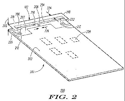
[00011] FIG. 2 depicts an exemplary embodiment of a substrate 201 supporting
the
antenna 102, the transceiver 104 and the controller 106 of the communication
device
100. The antenna 102 may be defined as a combination of antenna elements 204,
220,
222, 212, and 206, and a ground structure 202. The substrate 201 can be
represented
by a rigid printed circuit board (PCB) constructed with a common compound such
as
FR-4, or a flexible PCB made of a compound such as KaptonTM (trademark of
DuPont). The substrate 201 can comprise a multi-layer PCB having one layer as
a
ground structure 202 (or portions of the ground structure 202 dispersed in
multiple
layers of the PCB). The ground structure 202 can be planar, or a curved
surface in the
case of a flexible PCB. For convenience, the ground structure 202 will be
referred to
herein as a ground plane 202 without limiting the possibility that the ground
structure
-2-
CA 02670754 2009-05-26
WO 2008/070337 PCT/US2007/082590
can be curved or formed by several inter-coupled conducting sections that do
not
necessarily belong to the same or any substrate. The PCB can support
components
228 making up portions of the transceiver 104 and the controller 106. Suitable
ground
structures may be constructed from multiple inter-coupled layers or inter-
coupled
sections as well (for instance, clam shell or slider phones have ground
structures that
are realized by suitable interconnection of various sub-structures). The
extremities of
ground structure form an approximately rectangular shape having a length
dimension
and a width dimension, which may be average dimensions. In some phone designs,
such as a clam shell or slider phone, the length of the ground plane may
change as the
orientation of phone parts is changed. The shape may be approximately
rectangular
in that it may be, for example tapered or trapezoidal to fit a housing, and as
mentioned
above, may be curved to conform to a housing, and the edges may not be
straight or
smooth - for example when an edge of the ground plane has to bypass a feature
of a
housing such as a plastic mating pin or post.
[00012] The antenna 102 can comprise first and second elongated conductors
204,
206 that are substantially co-extensive and substantially aligned to each
other in
substantially parallel, planar or curved surfaces that are separated by a
substantially
uniform gap. One of the first and second conductors 204, 206 may be said to be
above
the other. The first and second elongated conductors 204, 206 can be flat
conductors
or can have a cylindrical cross-section (such as a wire), and may be curved or
be
serpentine so as to provide greater electrical length of the elongated
conductors 204,
206, and/or to form the elongated conductors 204, 206 around interfering
objects, the
curving or serpentining being substantially within the respective planar or
curved
surfaces. A length of each of the elongated conductors 204, 206 is defined as
the
average length of the two centerlines along the first and second conductors
204, 206,
while a physical extent is defined as the maximum distance along the elongated
direction of the first and second elongated conductors 204, 206. The planar or
curved
planes in which the first and second elongated conductors 204, 206 are
substantially
formed may substantially conform to the shape of a portion of a surface of a
housing
assembly carrying the communication device 100 of FIG. 1, and one or both of
the
first and second elongated conductors 204, 206 may be substantially formed
adjacent
to or on portion(s) of a surface of the housing assembly. The descriptions
-3-
CA 02670754 2009-05-26
WO 2008/070337 PCT/US2007/082590
"substantially aligned", "substantially parallel", "substantially uniform
gap",
"substantially within", "substantially conform", and "substantially formed",
mean
that, in some embodiments, the ratio of the closest separation (gap) and
largest
separation (gap) between the centerlines of the elongated conductors may be up
to
1.5:1 In some embodiments this gap variation ratio may be substantially less,
such as
1.2:1, or less than 1.05:1. The first and second elongated conductors 204, 206
can
have a contour 216-222 as shown in FIG. 2, which may be termed a "U' shape. In
the
illustration of FIG. 2, the first conductor 204 is co-planar with the ground
plane 202.
Alternatively, the first conductor 204 can be above or below (e.g., on a back
side of
the substrate 201) the ground plane 202. In some embodiments, the first and
second
conductors 204, 206 can be misaligned with respect to each other to some
extent
within their flat or curved planes. At or near opposing end points of the
lengths of the
first and second conductors 204, 206, conductors 212 can be orthogonally
coupled to
the first and second conductors 204, 206 thereby forming a gap 205 determined
by a
length of the conductors 212, and forming a corresponding electro-magnetic
field
region having a gap 205 of for example 2.5mm to 4mm when the operating
frequency
of the antenna is approximately 1-2 GHz. Gap 205 can also be formed by
suitably
shaped spacers and/or dielectric material (not shown) placed between the first
and
second conductors 204, 206, and the gap 205 may be substantially uniform or
may
differ along the extension of the antenna element 102, resulting in a gap
variation
ratio described herein above. When the first and second conductors 204, 206
are
formed in curved planes, the gap 205 is a substantially uniform gap. The
misalignment mentioned above and the variation of the gap mentioned above are
such
that the separation of the first and second elongated conductors 204, 206 is
within the
limit described above. In some embodiments, the average separation (the
average gap)
of the first and second conductors 204, 206 may approximately 20% of the
physical
extent described above, while in other embodiments, it may be substantially
smaller,
such as 5% or less than 1% of the physical extent.
[00013] The ground plane 202 is separated from the first conductor 204 by
separation 207 (in this example, a non-conducting portion of substrate 201).
The
ground plane 202 is also separated from the second conductor 204 by a
separation
(not illustrated in FIG. 2). These separations are such that the average value
of the
-4-
CA 02670754 2009-05-26
WO 2008/070337 PCT/US2007/082590
separations is no more than 25% of the physical extent of the first and second
elongated conductors 204, 206. A ground conductor 208 can couple the ground
plane
202 to the first conductor 204 near the center of the physical extent of the
first
conductor 204, such as within 5% (physical extent) of the physical center.
Alternatively, the ground conductor 208 can couple the ground plane 202 to the
second conductor 206 near the center of the physical extent of the second
conductor
206, within similar limits. A signal feed conductor couples a signal from an
active
device to the first conductor 204 and is connected to the first conductor 204
at
location 210, in an embodiment in which the ground conductor is coupled to the
first
conductor 204, near a physical center of the physical extent of the first
conductor,
such as within 5% (physical extent) of the physical center. The signal
conductor
comprises, for example, a combination of conductive trace and wire (not shown)
that
may pass through other layers and couples to a transmitter, receiver, or
transceiver
mounted on the substrate 201 on a layer isolated from the ground plane 202.
There is
a separation 226 between the feed point where the ground conductor 208 is
attached
to the first conductor 204 and the feed point 210 where the signal feed
conductor
attaches to the first conductor 204. This separation may be small (e.g., less
than 10%)
compared to the physical extent of the elongated first and second conductors
204,
206. In some embodiments, the ground and signal feed points may be on the same
side of the center point of the physical extent, but in many embodiments they
may be
on opposite sides of the center. As with the ground conductor 208, the signal
feed
conductor can alternatively be coupled to the second conductor 206. It should
be
appreciated that the length of the ground conductor 208 from the ground
structure 202
to the antenna 102 and the length of a signal feed conductor from the location
210
where it attaches to the antenna 102 need not be the same (assuming that the
signal
feed conductor is shielded over substantially its entire length). The spacial
path
traversed by these conductors may be arbitrary (again, assuming that the
signal feed
conductor is shielded over substantially its entire length). There may be
lumped or
distributed reactive and resistive elements, e.g., , distributed resistances,
capacitances,
and/or inductances caused by materials that are between the ground and signal
feed
points or the ground and signal feed conductors or between the signal feed
point or
signal feed conductor and ground, capacitors, and/or inductors between these
the
-5-
CA 02670754 2009-05-26
WO 2008/070337 PCT/US2007/082590
ground and signal feed points or between the signal feed point or signal feed
conductor and ground It should be noticed that the distance between the feed
points
where the ground and signal feed conductors couple to antenna element 102 and
the
distance between the points where the ground and signal conductor couple to
the
printed circuit board structure can be substsantially different from each
other. Also,
the tridimensional path of these conductors, especially the signal conductor,
can be
arbitrary, and there can be lumped or distributed reactive and resistive
elements, e.g.,
chip resistors, capacitors, or inductors, connected at one or more points
along either
one of these conductors. The width of the ground plane is defined to be a side
that is
most closely parallel to the elgonated direction of the elongated conductors
204, 206,
and the width is substantially similar to the physical extent of the elongated
conductors 204, 206, i.e., it is within plus or minus 15% of the physical
extent of the
elongated conductors. The two elongated conductors are approximately
symmetrical
with reference to a centerline of the ground plane (a line parallel to the
length of the
ground plane that divides the ground plane in half).
[00014] In some embodiments, another gap (not shown in FIG. 2) may be formed
in the first conductor 204 within the separation 226. Alternatively, the other
gap could
be formed in the second conductor 206 between the ground connection and signal
feed point when the ground conductor and signal feed are attached to the
second
conductor 206. Furthermore, resistive and reactive lumped or distributed
elements
may be placed or realized across said gaps.
[00015] FIGs. 3-4 depict electrical current flow and a corresponding spectral
reflection coefficient response of an antenna similar to antenna 102 of FIG.
2, for
which the first and second elongated conductors, when analyzed as two antenna
elements, are substantially congruent in an electrical sense, by which is
meant that the
two antenna elements exhibit substantially similar degree and nature of
coupling with
ground plane - thus providing substantially similar resonant frequency of
antenna
elements . In these circumstances, the antenna 102 can be analyzed as having
three
modes of operation: a first common mode 402, a differential mode 404, and a
second
common mode 406 as depicted in FIG. 3. The contribution of each mode to the
performance of the antenna is determined by, among other things, the frequency
of
the signal being radiated, the geometry of the antenna, and the electrical
congruity of
-6-
CA 02670754 2009-05-26
WO 2008/070337 PCT/US2007/082590
the two antenna elements. These modes occur simultaneously, with the radio
frequency characteristics of the antenna (spectral shape, bandwidth, beam
shape, etc)
being determined by a combined effect of the three modes. In some instances
(i.e.,
certain geometry and signal frequency) at least one mode may be excited so
negligibly that it might be described as non-existent. Shown in each mode of
FIG. 3 is
a dashed reference centerline. The first and second common modes are
distinguished
from the differential mode in that currents flow substantially symmetrical to
the
center lines of the first and second common modes and substantially anti-
symmetrical
to the differential mode. The second common mode is distinguished from the
first
common mode in that there is a phase reversal of current approximately mid-
stream
of the center reference line. There are several variable design parameters
that can
affect the characteristics of the modes of operation, including the spectral
shape and
the operating bandwidth of the antenna 102. These variables can include,
without
limitation, the size of the gap 205, the size of the separation 226 between
the signal
feed conductor 210 and the ground conductor 208, a geometric and/or impedance
asymmetry between the first and second conductors 204, 206, and a size of the
geometry of the ground plane 202. These variables can affect the electrical
congruence of the two antenna elements.
[00016] For example, as the gap 205 separating the first and second conductors
204, 206 increases, the spectrum of FIG. 4 will typically shift up in
frequency, and
vice-versa. As the separation 226 between signal feed conductor 210 and the
ground
conductor 208 decreases the resonant frequency of the first common mode 402
typically shifts down in frequency and its operating bandwidth widens, and the
operating frequency of each of the differential mode 404 and second common
mode
406 typically widens.
[00017] When an electrical non-congruence is created between the first and
second
conductors 204, 206, the frequency response of the antenna can be dramatically
changed,due to the effect of the electrical non-congruence on resonance of the
first
common mode. Electrical non-congruence between the conductors can be
accomplished in a number of ways, and results in a difference of the
characteristic
electrical lengths of the conductors. One example of such asymmetry is shown
in FIG.
5, which is described more fully below. In particular, in an embodiment
similar to
-7-
CA 02670754 2009-05-26
WO 2008/070337 PCT/US2007/082590
that shown in FIG. 5, the first common mode resonance can be made to be broad,
with
two resonant frequencies 602-604, as shown in FIG. 6, which have a
substantially
wider operating bandwidth 606 (880 MHz - 1.42 GHz with a return loss of less
than -
dB) than the spectrum in FIG. 4 This very wide operating range can be used for
applications such as software defined radio (SDR) and ultra wide bandwidth
radio
(UWB radio), or for digital video broadcasting - handhelds (DVB-H) with the
overall
dimensions of the antenna elements and ground plane adjusted for operation at
the
assigned frequency bands. It will be noted that the -10 dB bandwidth of the
first
mode of the antenna represented by FIG. 6 is approximately 49%, while the -10
dB
bandwidth of the first mode of the antenna represented by FIG. 4 is
approximately
10%. (bandwidth has been calculated by the conventional formula of (upper
frequency-lower frequency) divided by the square root of (upper frequency
times
lower frequency). Accordingly, it is shown that the -10 dB bandwidth of the
first
common mode of embodiments of antennas described herein has been broadened to
be approximately 5 times larger when electrical non-congruence is introduced
with
respect to embodiments of similar antennas having approximate electrical
congruence. Further experiments have established that even greater broadening
can be
achieved, such as a-l0d dB bandwidth of at least 0.5. Thus, electrical non-
congruence can provide a bandwidth of the first common mode of greater than
0.5.
[00018] Referring again to FIG. 5, the broadness of the first common mode can
be
accomplished in some embodiments by designing an electrical non-congruence of
the
antenna elements that is achieved by forming a geometric asymmetry between the
first and second conductors 204, 206 at portions 502-504 (refer to FIG. 5) of
the first
conductor 204 and portions 216-218 of the second conductor. The asymmetry
results
from portions 216-218 having less surface area than portions 502-504. The wide
operating frequency 606 shown in FIG. 6 results from each asymmetric portion
502-
504 having slightly different resonances. Alternatively, a geometric asymmetry
can be
achieved as shown in FIG. 2, by making the width 224 of the second conductor
206
larger than a similar section of the first conductor 204. A wide operating
frequency
606 similar to that shown in FIG. 6 can be obtained from appropriate
asymmetric
widths of the first and second conductors 204, 206. In yet another embodiment,
an
electrical non-congruence can be created by depositing dielectric material on
either of
-8-
CA 02670754 2009-05-26
WO 2008/070337 PCT/US2007/082590
the first and second conductors 204, 206 or placing a dielectric spacer
between
portions of said conductors. Combinations of these techniques to may be used
to
optimize the frequency range and improve the return loss of an operating
bandwidth
of the antenna.
[00019] The length of the ground plane 202 can be determined from a desired
lowest operating frequency and a fractional wavelength of the antenna 102. For
instance, from experimentation of the antenna 102 shown in FIG. 5 a ground
plane
length 202 of 11 cm provided a lowest operating frequency of 880 MHz (see ml).
At
this frequency, the wavelength of the antenna 102 can be calculated as 34cm
utilizing
the well-known relationship A = c / f. From this formula, a length of the
ground plane
202 can be determined to be approximately 1/3 (or 1 lcm/34cm) of the
wavelength of
the lowest operating frequency of the first common mode resonance of the
antenna
102. Thus, at a desired operating frequency of 500 MHz the ground plane 202
can be
calculated to have a length of approximately 18cm,
A = c =60cm --> Ground Plane = 0.3 * A = 0.3 * 60cm = l 8cm .
500MHz -
The width of the ground plane can be approximately 1/4 of the length
calculated above.
Thus, as the length of the ground plane 202 is increased the lowest operating
frequency of the first common mode decreases, and vice-versa. When variations
according to embodiments described herein (such as electrical non-congruence,
the
size of the gap between the elongated elements, a difference between the
electrical
length of the elongated elements, and the separation of the elongated elements
from
the ground plane) are taken into account, the length of the ground plane may
be
between 0.2 and 1.0 times the wavelength of the lowest operating frequency,
and the
width of the ground plane may be between 0.2 and 1.0 times the length of the
ground
plane.
[00019] A matching circuit can be used to couple the antenna 102 to the
transceiver
104. In a supplemental embodiment, a matching impedance between an LC matching
circuit of the transceiver 104 and the antenna 102 can be varied by appending
conductor 508 between the first and second conductors 204, 206, or by varying
a
distance between the feed 210 and the ground conductor 208. Thus, conductor
508
-9-
CA 02670754 2009-05-26
WO 2008/070337 PCT/US2007/082590
can be used to match the impedance of the antenna 102 over a wide operating
frequency band 606 as shown in FIG. 6.
[00020] The foregoing embodiments of the antenna 102 such as those illustrated
in
FIGs. 2 and 5 can provide a wideband internal or external antenna design with
a wide
operating bandwidth which can be contoured to a housing assembly (not shown)
of
the communication device 100 if desired. It would be evident to one of
ordinary skill
in the art that the foregoing embodiments can be modified without departing
from the
scope of the present invention. For example, the first and second conductors
204, 206
and conductors 212 can be formed from a contiguous conductor (such as a wire
or
folded form cut from one piece of sheet metal) having first and second ends
coupled
to the signal feed and ground conductors 208-210.
[00021] In one embodiment, the antenna has a lowest frequency of operations
that
is approximately 820 MHz, and the corresponding wavelength is approximately 37
cm.. The gap between the first and second elongated conductors averages
about 0.01 *wavelength, the gap variation ratio is less than 1.5: l, the first
and second
average separations are each less than 0.03 *wavelength, the ground plane has
an
average length that is about 0.3 *wavelength, and the ground plane has an
average
width of 0.1 *wavelength.
[00022] In this same embodiment, the antenna the wideband response is 820 -
1480
MHz at -10 dB, the gap between the first and second elongated conductors
averages about 4 mm, a gap variation ratio is less than 1.5:1, the first and
second
average separations are each less than 10 mm, the ground plane has an average
length
that is about 95 mm, and the ground plane has an average width of 40 mm.
[00023] In another embodiment, the antenna has a lowest frequency of
operations
of approximately 1.0 GHz, a corresponding wavelength is approximately 30 cm.
The
average gap between the first and second elongated conductors is approximately
0.008*wavelength, a gap variation ratio is less than 1.5:1, the first and
second
average separations are each less than 0.03 *wavelength, the ground plane has
an
average length that is approximately 0.3 *wavelength, and the ground plane has
an
average width of 0.2*wavelength.
[00024] In this other embodiment, the lowest frequency of operations is
approximately 1 GHz, the corresponding wavelength is approximately 30 cm., the
-10-
CA 02670754 2009-05-26
WO 2008/070337 PCT/US2007/082590
average gap between the first and second elongated conductors is about 2.5 mm,
a gap
variation ratio is less than 1.5:1, the first and second average separations
are each less
than 10 mm, the ground plane has an average length that is about 90 mm., and
the
ground plane has an average width of 50 mm.
[00025] Accordingly, the specification and figures associated with these
embodiments are to be regarded in an illustrative rather than a restrictive
sense, and
all modifications are intended to be included within the scope of the claims
described
below. The benefits, advantages, solutions to problems, and any element(s)
that may
cause any benefit, advantage, or solution to occur or become more pronounced
are not
to be construed as a critical, required, or essential features or elements of
any or all
the claims. The invention is defined solely by the appended claims including
any
amendments made during the pendency of this application and all equivalents of
those
claims as issued.
[00026] The Abstract of the Disclosure is provided to allow the reader to
quickly
ascertain the nature of the technical disclosure. It is submitted with the
understanding
that it will not be used to interpret or limit the scope or meaning of the
claims. In
addition, in the foregoing Detailed Description, it can be seen that various
features are
grouped together in a single embodiment for the purpose of streamlining the
disclosure. This method of disclosure is not to be interpreted as reflecting
an
intention that the claimed embodiments require more features than are
expressly
recited in each claim. Rather, as the following claims reflect, inventive
subject matter
lies in less than all features of a single disclosed embodiment. Thus the
following
claims are hereby incorporated into the Detailed Description, with each claim
standing on its own as a separately claimed subject matter.
-11-