Note: Descriptions are shown in the official language in which they were submitted.
CA 02670809 2009-07-17
WO 2008/104059 PCT/CA2008/000357
METHOD FOR FORMING A FILM ON A SUBSTRATE
FIELD OF THE INVENTION
The present invention relates to a method for forming a
silicon carbide based film on a substrate.
BACKGROUND OF THE INVENTION
There are presently available a variety of methods and
source compounds used for forming an amorphous silicon
carbide based film on a substrate, some of which are
discussed herein.
For example, gaseous source compounds can be used in a
chemical vapor deposition (CVD) process to deposit a film on
a semiconductor. Yaol teaches a method of producing a SiC
based film requiring the use of silane and hydrocarbon
gases. However, the use of an extremely pyrophoric gas such
as silane gas in such a method requires costly precautionary
handling procedures. The method also requires addition of
hydrogen to the gaseous mixture or an elaborate means for
controlling the temperature of the reactant gases due to the
difference in temperature of dissociation between the silane
and hydrocarbon gases.
A CVD process may be employed with a liquid polymeric source
or a source compound that is dissolved or mixed into a
solvent medium, such as described by Gardiner et a1.2 or
Chayka3. However, most liquid based polymeric sources are
flammable or pyrophoric, thus requiring special handling.
Furthermore, Pitcher et a1.4 teach that a treatment time in
excess of 48 hours and a pyrolysis time in excess of 24
hours are required.
Starfire Systemss has developed a method of producing
stoichiometric SiC films from stoichiometric source
1
CA 02670809 2009-07-17
WO 2008/104059 PCT/CA2008/000357
compounds. In this method, the two sources (CVD-2000TM and
CVD-4000TM) are liquid, flammable (flash point 9 C, 51 C) , and
air and moisture sensitive.
Goela et al.6 teach a CVD process using a chlorine-containing
source compound either in a gas or liquid form. However,
the chlorine containing source compound forms corrosive and
toxic hydrogen chloride fumes upon contact with moisture,
which significantly complicates storage, disposal, handling,
and pumping of such material.
Spin coating methods have been used wherein a polymeric
source is dissolved in a solvent and then applied to a
substrate by spinning, dipping, spraying, swabbing, or
brushing. Subsequently, pyrolysis of the source on the
substrate occurs at an elevated temperature, for example
1000 C or more for several hours (see Moehle et al.'). In
addition to limitations of substrate shape and orientation
in the spin coating method, the high temperature of
pyrolysis limits the type of material used as the substrate.
The method also results in a high density of defects (voids)
due to outgassing of solvent during pyrolysis, uneven film
thickness due to the spin coating, and cracks due to
shrinkage of the films.
Ruppel et al.8 teaches a method of coating a substrate by
sputtering, which produces a non-stoichiometric film. A
good deal of heat is generated as the sputtering rate
increases, which may destroy the substrate, for example when
the substrate is made from plastic. Further, film produced
by sputtering is usually hydrogen free, which is a major
disadvantage for semiconductor applications.
Silicon carbide based films such as those described above
have been used for reduction of the surface recombination
velocity, also described as surface passivation, of silicon
2
CA 02670809 2009-07-17
WO 2008/104059 PCT/CA2008/000357
semiconductor samples such as silicon wafer based solar
cells. Films having better passivation characteristics
would increase the efficiency of these devices. However,
due to the high cost and toxicity of gases that are often
involved in making these devices, production of such
passivation layers for devices may not always be viable.
SUMMARY OF THE INVENTION
According to one aspect of the present invention, there is
provided a method for forming a film on a substrate
comprising: heating a solid organosilane source in a heating
chamber to form volatile fragments of the solid organosilane
source (also referred to herein as the gaseous precursor);
transferring the gaseous precursor to a deposition chamber
containing the substrate; and reacting the gaseous precursor
using an energy source to form a film on the substrate. In
an embodiment, the energy source is plasma. In another
embodiment, the transferring step may comprise using a
carrier gas. In yet another embodiment, the method may
further comprise mixing the gaseous precursor with a
reactant gas prior to the reacting step; the gaseous
precursor and the reactant gas may be admixed prior to
transfer to the deposition chamber, or the gaseous precursor
and reactant gas can both be transferred separately to the
deposition chamber. In still another embodiment, the
deposition chamber is within a reactor and the heating
chamber is external to the reactor. In yet another
embodiment, the deposition chamber and the heating chamber
are both within a reactor.
According to another aspect of the present invention, there
is provided a method for surface passivation of a silicon
based semiconductor, comprising depositing a film on the
surface of the semiconductor according to the method
3
CA 02670809 2009-07-17
WO 2008/104059 PCT/CA2008/000357
described herein, the semiconductor and deposited film being
optionally annealed.
According to still another aspect of the present invention,
there is provided a container comprising a gaseous precursor
produced by heating a solid organosilane source for use in a
method for forming a film on a substrate.
BRIEF DESCRIPTION OF THE DRAWINGS
In the accompanying drawings, which illustrate an exemplary
embodiment of the present invention:
Figure 1 is a graph from Elastic Recoil Detection (ERD) of a
a-SiCN:H sample;
Figure 2 is a graph from Elastic Recoil Detection (ERD) of a
a-SiCN:H sample;
Figure 3 is a graph from Elastic Recoil Detection (ERD) of a
a-SiCN:H sample;
Figure 4 is the output from the measurement of lifetime
using the -PCD technique;
Figure 5(a) is the output from the effective lifetime
measurement of a FZ Si wafer passivated by a-SiCN:H using
the Sinton technique;
Figure 5(b) is a graph showing the implied open circuit
voltage of a Si substrate as a function of light intensity;
Figure 6 is a graph of effective lifetime of an a-SiCN:H
coated FZ Si wafer as a function of film thickness;
Figure 7 is graph of effective lifetime of the a-SiCN:H
films as a function of silicon to nitrogen ratio;
4
CA 02670809 2009-07-17
WO 2008/104059 PCT/CA2008/000357
Figure 8 is an optical transmission spectrum of the a-SiCN:H
films deposited on quartz at 400 C using PDMS single source
and NH3 added to the gas flow. Four different samples were
prepared to confirm the process repeatability. The
thickness of the a-SiCN:H films is typically 80 5nm;
Figure 9 is a graph of absorption coefficient and wavelength
for films prepared by the method described herein and prior
art films; and
Figure 10 is a schematic of a solar cell with multiple
optical coatings on each major surface, each having a
refractive index n', nz, nX, nl, nz or ny.
DETAILED DESCRIPTION OF THE INVENTION
The present invention relates to a method for forming a film
on a substrate comprising heating a solid organosilane
source in a heating chamber to form a gaseous precursor,
transferring the gaseous precursor to a deposition chamber,
and reacting the gaseous precursor using an energy source to
form the film on the substrate.
The method of the present invention may produce near-
stoichiometric SiC films on a substrate even when the Si:C
ratio in the solid organosilane source is non-
stoichiometric. If the solid organosilane is PDMS, the
method may require less silicon-carbon bond formation on the
surface of the substrate, since Si-C bonds in the pre-cursor
gas can be obtained during the Kumada re-arrangement
preceding the deposition of the film. For other organosilane
solids (e.g. polycarbosilane), the method may require less
silicon-carbon bond formation on the surface of the
substrate, since Si-C bonds can be provided in the gaseous
precursor obtained from the organosilane solid, which is
volatised preceding the deposition of the film. Further,
5
CA 02670809 2009-07-17
WO 2008/104059 PCT/CA2008/000357
the method does not require any solvents thereby eliminating
cracking, shrinking, voids or porosity formation due to
outgassing of solvents.
Solid organosilane source
A solid organosilane source refers to compounds that
comprise Si, C and H atoms, and that are solid at room
temperature and pressure.
The solid organosilane source may, in one embodiment, be a
silicon-based polymer comprising Si-C bonds that are
thermodynamically stable during heating in the heating
chamber. In one embodiment, the silicon-based polymer has a
monomeric unit comprising at least one silicon atom and two
or more carbon atoms. The monomeric unit may further
comprise additional elements such as N, 0, F, B, P, or a
combination thereof. In another embodiment, the polymeric
source is a polysilane or a polycarbosilane.
The polysilane compound can be any solid polysilane compound
that can produce gaseous organosilicon compounds when
pyrolysed, i.e. chemical decomposition of the solid
polysilane by heating in an atmosphere that is substantially
free of molecular oxygen. In one embodiment, the solid
polysilane compound comprises a linear or branched
polysilicon chain wherein each silicon is substituted by one
or more hydrogen atoms, C1-C6 alkyl groups, phenyl groups or
-NH3 groups. In a further embodiment, the linear or branched
polysilicon chain has at least one monomeric unit comprising
at least one silicon atom and one or more carbon atoms. In
another embodiment, the linear or branched polysilicon chain
has at least one monomeric unit comprising at least one
silicon atom and two or more carbon atoms.
Examples of solid organosilane sources include silicon-based
polymers such as polydimethylsilane (PDMS) and
6
CA 02670809 2009-07-17
WO 2008/104059 PCT/CA2008/000357
polycarbomethylsilane (PCMS), and other non-polymeric
species such as triphenylsilane or nonamethyltrisilazane.
PCMS is commercially available (Sigma-Aldrich) and can have,
for example, an average molecular weight from about 800
g/mol to about 2000 g/mol. PDMS is also commercially
available (Gelest, Morrisville, P.A. and Stem Chemical,
Inc., Newburyport, M.A.) and it can have, for example, an
average molecular weight from about 1100 to about 1700.
PDMS is known as a polymer able to yield polycarbosilane.
Use of PDMS as a source compound is advantageous in that (a)
it is very safe to handle with regard to storage and
transfer, (b) it is air and moisture stable, a desirable
characteristic when using large volumes in industrial
environment, (c) no corrosive components are generated in an
effluent stream resulting from PDMS being exposed to CVD
process conditions, and (d) PDMS provides its own hydrogen
supply by virtue of its hydrogen substituents and yields
dense amorphous SiC at temperatures as low as 50 C.
In another embodiment, the solid organosilane source may
have at least one label component, the type, proportion and
concentration of which can be used to create a chemical
"fingerprint" in the obtained film that can be readily
measured by standard laboratory analytical tools, e.g.
Secondary Ion Mass Spectrometry (SIMS), Auger Electron
Spectrometry (AES), X-ray photoelectron spectroscopy (XPS).
In one embodiment, the solid organosilane source can contain
an isotope label, i.e. a non-naturally abundant relative
amount of at least one isotope of an atomic species
contained in the solid organosilane source, e.g. C13 or C14
This is referred to herein as a synthetic ratio of isotopes.
Formation of the gaseous precursor species
7
CA 02670809 2009-07-17
WO 2008/104059 PCT/CA2008/000357
In one embodiment, the solid organosilane source may be
added to the heating chamber in a batch or continuous manner
as a powder, pellet, rod or other solid form. Optionally,
the solid organosilane source may be mixed with a second
solid polymer in the heating chamber. In batch addition,
the solid organosilane source compound may be added, for
example, in an amount in the range of from 1 mg to 10 kg,
although larger amounts may also be used.
In one embodiment the heating chamber is purged, optionally
under vacuum, after the solid organosilane source has been
added to replace the gases within the chamber with an inert
gas, such as argon or helium. The chamber can be purged
before heating is commenced, or the temperature within the
chamber can be increased during, or prior to, the purge.
The temperature within the chamber during the purge should
be kept below the temperature at which evolution of the
gaseous precursor species commences to minimise losses of
product.
The production of the gaseous precursor from the solid
organosilane source is achieved through a pyrolysis step,
which can encompass one or more different types of reactions
within the solid. The different types of reactions, which
can include e.g. volatisation of the solid organosilane
source or decomposition/rearrangement of the solid
organosilane into a new gaseous organosilane species, will
depend on the nature of the solid organosilane source, and
these reactions can also be promoted by the temperature
selected for the pyrolysis step. For embodiments where the
solid organosilane source is a polysilane, the gaseous
precursor species can be obtained through a process as
described in U.S. provisional application S/N 60/990,447
filed on November 27, 2007, the disclosure of which is
incorporated herein by reference in its entirety.
8
CA 02670809 2009-07-17
WO 2008/104059 PCT/CA2008/000357
The heating of the solid organosilane source in the heating
chamber may be performed by electrical heating, UV
irradiation, IR irradiation, microwave irradiation, X-ray
irradiation, electronic beams, laser beams or the like.
The heating chamber is heated to a temperature in the range
of, for example, from about 50 to about 700 C, from about 100
to about 700 C, from about 150 to about 700 C, from about 200
to about 700 C, from about 250 to about 700 C, from about 300
to about 700 C, from about 350 to about 700 C, from about 400
to about 700 C, from about 450 to about 700 C, from about 500
to about 700 C, from about 550 to about 700 C, about 600 to
about 700 C, from about 650 to about 700 C, from about 50 to
about 650 C, from about 50 to about 600 C, from about 50 to
about 550 C, from about 50 to about 500 C, from about 50 to
about 450 C, from about 50 to about 400 C, from about 50 to
about 350 C, from about 50 to about 300 C, from about 50 to
about 250 C, from about 50 to about 200 C, from about 50 to
about 150 C, from about 50 to about 100 C, from about 100 to
about 650 C, from about 150 to about 600 C, from about 200 to
about 550 C, from about 250 to about 500 C, from about 300 to
about 450 C, from about 350 to about 400 C, from about 475 to
about 500 C, about 50 C, about 100 C, about 150 C, about
200 C, about 250 C, about 300 C, about 350 C, about 400 C,
about 450 C, about 500 C, about 550 C, about 600 C, about
650 C, or about 700 C. A higher temperature can increase the
rate at which the gaseous precursor compounds are produced
from the solid organosilane source.
In one embodiment, the heating chamber is heated at a rate
of up to 150 C per hour until the desired temperature is
reached, at which temperature the chamber is maintained. In
another embodiment, the temperature is increase to a first
value at which pyrolysis proceeds, and then the temperature
9
CA 02670809 2009-07-17
WO 2008/104059 PCT/CA2008/000357
is changed on one or more occasion, e.g. in order to vary
the rate at which the mixture of gaseous precursor compound
is produced or to vary the pressure within the chamber.
In one embodiment the temperature and pressure within the
heating chamber are controlled, and production of the
gaseous precursor can be driven by reducing the pressure, by
heating the organosilane source, or by a combination
thereof. Selection of specific temperature and pressure
values for the heating chamber can also be used to control
the nature of the gaseous precursor obtained.
In the embodiment where the solid organosilane source is a
polysilane, one possible pyrolisis reaction leads to the
formation of Si-Si crosslinks within the solid polysilane,
which reaction usually takes place up to about 375 C.
Another possible reaction is referred to as the Kumada
rearrangement, which typically occurs at temperatures
between about 225 C to about 350 C, wherein the Si-Si
backbone chain becomes a Si-C-Si backbone chain. While this
type of reaction is usually used to produce a non-volatile
product, the Kumada re-arrangement can produce volatile
polycarbosilane oligomers, silanes and/or methyl silanes.
While the amount of gaseous species produced by way of the
Kumada rearrangement competes with the production of non-
volatile solid or liquid polycarbosilane, the production of
such species, while detrimental to the overall yield, can
prove a useful aspect of the gas evolution process in that
any material, liquid or solid that is left in the heating
chamber is in some embodiments turned into a harmless and
safe ceramic material, leading to safer handling of the
material once the process is terminated.
For the embodiment where the solid organosilane is a
polysilane, the pressure within the heating chamber can be
maintained at a predetermined pressure or within a
CA 02670809 2009-07-17
WO 2008/104059 PCT/CA2008/000357
predetermined pressure range in order to provide a desired
molar ratio of gaseous precursor compounds in the produced
gaseous mixture. Generally, maintaining a high pressure,
e.g. 600 to 900 psi, favours the production of gaseous
precursor species having a lower molecular weight (e.g. a
lower number of silicon atoms), while maintaining a lower
pressure, e.g. 100 to 250 psi, favours the production of
gaseous organosilicon species having a higher molecular
weight (e.g. higher number of silicon atoms).
Gaseous precursor species
Generally, the gaseous precursor comprises a mixture of
volatile fragments of the solid organosilane source. In the
embodiment where the solid organosilane precursor is a
polysilane, the gaseous precursor species is a mixture of
gaseous organosilicon compounds, i.e. compounds comprising
silicon, carbon and hydrogen atoms that are in the gas phase
at 20 C and 20 psi.
In one embodiment, the mixture of gaseous organosilicon
compounds comprises one of more gases selected from a
gaseous silane, a gaseous polysilane, or a gaseous
polycarbosilane. In another embodiment, substantially all
of the gaseous organosilicon compounds produced within the
mixture comprise from 1 to 4 silicon atoms. By gaseous
silane is meant a compound comprising a single silicon atom,
by gaseous polysilane is meant a compound comprising two or
more silicon atoms wherein the silicon atoms are covalently
linked (e.g. Si-Si), and by gaseous polycarbosilane is meant
a compound comprising two or more silicon atoms wherein at
least two of the silicon atoms are linked through a non-
silicon atom (e.g. Si-CH2-Si) 11
CA 02670809 2009-07-17
WO 2008/104059 PCT/CA2008/000357
In a further embodiment, the gaseous organosilicon compound
can be a gaseous polycarbosilane of formula:
Si (CH3) n(H) m- [ (CH2) -Si (CH3) p(H) q] x-Si (CH3) n'(H) m,
wherein n, m, n' and m' independently represent an integer
from 0 to 3, with the proviso that n + m = 3 and n' + m' =
3, p and q independently represent an integer from 0 to 2,
with the proviso that p + q = 2 for each silicon atom, and x
is an integer from 0 to 3.
Examples of gaseous silanes and gaseous polycarbosilanes
include silane, dimethyl, trimethyl silane, tetramethyl
silane, [Si (CH3) (H) 2] -CH2- [Si (CH3) z (H) ] , [Si (CH3) z (H) ] -CH2-
[Si (CH3) 2 (H) ] , [Si (CH3) 3] -CH2- [Si (CH3) 2 (H) ] , [Si (CH3) 2 (H) ] -
CH2-
[Si (CH3) 21 -CH2- [Si (CH3) 3] , [Si (CH3) (H) z] -CH2- [Si (CH3) 21 -CHZ-
[Si (CH3) (H) 21 , [Si (CH3) (H) 2] -CH2- [Si (CH3) 21 -CH2- [Si (CH3) 2 (H) ]
[Si (CH3) 2 (H) ] -CH2- [Si (CH3) z] -CH2- [Si (CH3) 2 (H) ] , [Si (CH3) 2 (H)
] -
CH2- [Si (CH3) 2] -CH2- [Si (CH3) 2] -CH2- [Si (CH3) 2 (H) ] , [Si (CH3) (H)
2] -
CH2- [Si (CH3) 2] -CHz- [Si (CH3) 2] -CH2- [Si (CH3) 2 (H) ] , [Si (CH3) (H)
z] -
-
CH2 - [Si (CH3) 2] -CH2- [Si (CH3) 2] -CH2- [Si (CH3) (H) 2] , and [Si (H) 31
CH2 - [Si (CH3) 2] -CH2- [Si (CH3) 2] -CH2- [Si (CH3) (H) 2]
After forming the gaseous precursor, it may be used
immediately or stored under appropriate temperature and
pressure conditions for later use. The process may be
interrupted at this stage since the heating chamber may be
external to the reactor.
Addition of a reactant gas
After heating, the gaseous precursor formed may be mixed
with a reactant gas in the heating chamber, the deposition
chamber or in a gas mixing unit. In one embodiment, the
reactant gas may be in the form of a gas that is
commercially available, and the gas is provided directly to
the system. In another embodiment, the reactant gas is
12
CA 02670809 2009-07-17
WO 2008/104059 PCT/CA2008/000357
produced by heating a solid or liquid source comprising any
number of elements, such as N, 0, F, B, P, or a combination
thereof.
For example, the reactant gas may be produced by heating a
solid source comprising phosphorous such as
triphenylphosphine (C6H5)3P; a solid source comprising
nitrogen such as tris(pyrazol-1-yl)methane); or a solid
source comprising boron such as borane t-butylamine
(CH3) 3CNH2:BH3, triethanolamineborate B(OCH2CH2) 3N, borane
dimethylamine (CH3) 2NH:BH3, or triphenylboron B(C6H5) 3. Aida
et a1.9 reported the use of triphenylphosphine (C6H5)3P as a
good source of phosphine for doping a-SiC prepared by RF
sputtering of Si target in the presence of a (C6H5)3P disk.
In another example, the reactant gas may be produced by
heating a liquid source comprising fluorine such as
difluorobenzene (C6H4F2); a liquid source comprising
phosphorous such as triethylphosphine (C2H5)3P,
dimethylphenylphosphine (CH3) z (C6H5) P, or
tris(trimethylsilyl)phosphine [(CH3)3Si]3P; or a liquid
source comprising boron such as tris(trimethylsiloxy)boron
[(CH3)3SiO]3B. Riedel et al.10 reported doping a SiCN ceramic
using polymeric source
tris[[dichloromethylsilyl]ethyl]boron) and Ramakrishnan et
al.ll reported using polyhydridomethlsilazane (NCP 200T"') and
tris[[dichloromethylsilyl]ethyl]borane polymer precursors as
p-type dopant for SiCN ceramics.
In still another example, the reactant gas may be a nitrogen
based gas such as NH3, N2, or NC13; an oxygen based gas such
as CO, 02, 03, C02; a fluorine based gas such as CF4, C4F8,
CH2F2, NF3, C2F6, C3F8, CHF3, C2F4, C3F6, or a combination
thereof; a boron based gas such as BH3, B2H6, BC13, B2C16; or
a phosphorous based gas such as PH3 or PC13.
13
CA 02670809 2009-07-17
WO 2008/104059 PCT/CA2008/000357
In an embodiment, the reactant gas may also comprise Al, B,
Ge, Ga, P, As, N, In, Sb, S, Se, Te, In and Sb.
Configuration of heating and deposition chambers
The method of the present invention may be carried with a
variety of system configurations, such as a heating chamber
and a deposition chamber; a heating chamber, a gas mixing
unit and a deposition chamber; a heating chamber, a gas
mixing unit and a plurality of deposition chambers; or a
plurality of heating chambers, a gas mixing unit and at
least one deposition chamber. In a preferred embodiment,
the deposition chamber is within a reactor and the heating
chamber is external to the reactor.
For high throughput configurations, multiple units of the
heating chamber may be integrated. Each heating chamber in
the multiple-unit configuration may be of a relatively small
scale in size, so that the mechanical construction is simple
and reliable. All heating chambers may supply common gas
delivery, exhaust and control systems so that cost is
similar to a larger conventional reactor with the same
throughput. In theory, there is no limit to the number of
reactors that may be integrated into one system.
The method of the present invention may also utilize a
regular mass flow or pressure controller to more accurately
deliver appropriate process demanded flow rates. The
gaseous precursor may be transferred to the deposition
chamber in a continuous flow or in a pulsed flow.
The method of the present invention may in some embodiments
utilize regular tubing without the need of special heating
of the tubing as is the case in many liquid source CVD
processes in which heating the tubing lines is essential to
eliminate source vapor condensation, or earlier
decomposition of the source.
14
CA 02670809 2009-07-17
WO 2008/104059 PCT/CA2008/000357
Deposition chamber
When it is desired to form a film, the substrate is placed
into the deposition chamber, which is evacuated to a
sufficiently low pressure, and the gaseous precursor and
optionally the reactant and carrier gas are introduced
continuously or pulsed. Any pressure can be selected as
long as the energy source selected to effect the deposition
can be used at the selected pressure. For example, when
plasma is used as the energy source, any pressure under
which a plasma can be formed is suitable. In embodiments of
the present invention the pressure can be from about 50 to
about 500 mTorr, from about 100 to about 500 mTorr, from
about 150 to about 500 mTorr, from about 200 to about
500 mTorr, from about 200 to about 500 mTorr, from about 250
to about 500 mTorr, from about 300 to about 500 mTorr, from
about 350 to about 500 mTorr, from about 400 to about 500
mTorr, from about 450 to about 500 mTorr, from about 50 to
about 450 mTorr, from about 50 to about 400 mTorr, from
about 50 to about 350 mTorr, from about 50 to about
300 mTorr, from about 50 to about 250 mTorr, from about 50
to about 200 mTorr, from about 50 to about 150 mTorr, from
about 50 to about 100 mTorr, from about 100 to about
450 mTorr, from about 150 to about 400 mTorr, from about 200
to about 350 mTorr, from about 250 to about 300 mTorr, from
about 50 mTorr to about 5 Torr, from about 50 mTorr to about
4 Torr, from about 50 mTorr to about 3 Torr, from about
50 mTorr to about 2 Torr, from about 50 mTorr to about
1 Torr, about 50 mTorr, about 100 mTorr, about 150 mTorr,
about 200 mTorr, about 250 mTorr, about 300 mTorr, about
350 mTorr, about 400 mTorr, about 450 mTorr, about
500 mTorr, about 1 Torr, about 2 Torr, about 3 Torr, about
4 Torr, or about 5 Torr.
CA 02670809 2009-07-17
WO 2008/104059 PCT/CA2008/000357
The substrate is held at a temperature in the range of, for
example, from about 25 to about 500 C, from about 50 to about
500 C, from about 100 to about 500 C, from about 150 to about
500 C, from about 200 to about 500 C, from about 250 to about
500 C, from about 300 to about 500 C, from about 350 to about
500 C, from about 400 to about 500 C, from about 450 to about
500 C, from about 25 to about 450 C, from about 25 to about
400 C, from about 25 to about 350 C, from about 25 to about
300 C, from about 25 to about 250 C, from about 25 to about
200 C, from about 25 to about 150 C, from about 25 to about
100 C, from about 25 to about 50 C, from about 50 to about
450 C, from about 100 to about 400 C, from about 150 to about
350 C, from about 200 to about 300 C, about 25 C, about 50 C,
about 100 C, about 150 C, about 200 C, about 250 C, about
300 C, about 350 C, about 400 C, about 450 C, or about 500 C.
Any system for conducting energy induced chemical vapor
deposition (CVD) may be used for the method of the present
invention. Other suitable equipment will be recognized by
those skilled in the art. The typical equipment, gas flow
requirements and other deposition settings for a variety of
PECVD deposition tools used for commercial coating solar
cells can be found in True Blue, Photon International, March
2006 pages 90-99 inclusive, the contents of which are
enclosed herewith by reference.
The energy source in the deposition chamber may be, for
example, electrical heating, hot filament processes, UV
irradiation, IR irradiation, microwave irradiation, X-ray
irradiation, electronic beams, laser beams, plasma, or RF.
In a preferred embodiment, the energy source is plasma.
For example, suitable plasma deposition techniques may be
plasma enhanced chemical vapor deposition (PECVD), radio
frequency plasma enhanced chemical vapor deposition (RF-
PECVD), electron-cyclotron-resonance plasma-enhanced
16
CA 02670809 2009-07-17
WO 2008/104059 PCT/CA2008/000357
chemical-vapor deposition (ECR-PECVD), inductively coupled
plasma-enhanced chemical-vapor deposition (ICP-ECVD), plasma
beam source plasma enhanced chemical vapor deposition (PBS-
PECVD), or combinations thereof. Furthermore, other types
of deposition techniques suitable for use in manufacturing
integrated circuits or semiconductor-based devices may also
be used.
Substrate
A wide variety of substrate materials may be used since the
formation of the film on the substrate occurs at a
relatively low temperature. Suitable materials for the
substrate may be, for example, metallic and inorganic
materials, elementary silicon, carbon and ceramic materials
such as silicon carbide, silicon nitride, alumina, quartz,
glass or plastic, as well as heat-resistance synthetic
resins such as fluorocarbon polymers or polyamide resins.
In an embodiment, the substrate is a FZ Si(100) wafer.
The film of the present invention is particularly applicable
to solar cells fabricated from silicon. In this context the
film can be applied to amorphous, crystalline, or
polycrystalline silicon as well as n-doped, p-doped, or
intrinsic silicon. When used as an antireflective coating,
the film can be applied to the external n-doped and/or p-
doped surfaces of a solar cell to optimally minimise
reflections from these surfaces and to reduce the absorption
0.of the light in the film to below 1%.
Films
The film formed on the substrate may have the chemical
formula SiXCy wherein x and y may be, for example, from about
0.2 to about 0.8, from about 0.3 to about 0.8, from about
0.4 to about 0.8, from about 0.5 to about 0.8, from about
17
CA 02670809 2009-07-17
WO 2008/104059 PCT/CA2008/000357
0.6 to about 0.8, from about 7 to about 0.8, from about 0.2
to about 0.7, from about 0.2 to about 0.6, from about 0.2 to
about 0.5, from about 0.2 to about 0.4, from about 0.2 to
about 0.3, from about 0.3 to about 0.7, from about 0.4 to
about 0.6, about 0.2, about 0.3, about 0.4, about 0.5, about
0.6, about 0.7, or about 0.8. In a preferred embodiment, x
and y is about 0.5. The film may further comprise other
elements such as N, 0, F, B, P, or a combination thereof.
In an embodiment, the film may be a silicon carbide (SiC), a
silicon carbofluoride (SiCF), a silicon carbonitride (SiCN),
a silicon oxycarbide (SiOC), a silicon oxycarbonitride
(SiOCN), a silicon carboboride (SiCB), a silicon
carbonitroboride (SiCNB), a silicon carbophosphide (SiCP),
or a combination thereof. The film may be multilayered or
it may have a gradient of composition, e.g. a silicon
oxycarbonitride film where the oxygen concentration varies
at different thicknesses within the film.
For embodiments where the energy used during the deposition
is plasma, e.g. for PE-CVD, the values of x and y may be
controlled by suitably selecting conditions for (1) the
generation of the plasma, (2) the temperature of the
substrate, (3) the power and frequency of the reactor, (4)
the type and amount of gaseous precursor introduced into the
deposition chamber, and (5) the mixing ratio of gaseous
precursor and reactant gas.
For example, the silicon:carbon ratio of the silicon carbide
layer is tunable in that it may be varied as a function of
the RF power. The silicon:carbon ratio may be in a range of
about 1:2 to about 2:1. For example, the silicon:carbon
ratio in a silicon carbide layer formed at RF power of 900 W
is about 0.94:1, while silicon:carbon ratio of a silicon
carbide layer formed at RF power of 400 W is 1.3:1. A
18
CA 02670809 2009-07-17
WO 2008/104059 PCT/CA2008/000357
stoichiometric silicon carbide layer may be formed at RF
power of about 700 W.
The silicon:carbon ratio may also be varied as a function of
substrate temperature. More particularly, as the substrate
temperature is increased, the silicon:carbon ratio in the
deposited silicon carbide layer decreases.
The silicon:carbon ratio is also tunable as a function of
the composition of the gas mixture during SiC layer
formation.
The films produced by the method described herein have
improved properties, such as excellent passivation, low
mechanical stress, low absorption coefficient of light and a
controllable refractive index.
These improved properties can be used to minimize some of
the limitations which negatively affect solar cell
efficiency, which limitations include front surface
reflection; optical losses, e.g. those due to randomly
textured surface, especially in the shorter wavelength
region; and internal parasitic losses, such as those due to
random texture, Si02 AR, metallization design and absorption
of light in the metal contact.
These films my also be used as optical coatings, e.g. as
anti-scratch and/or anti-reflective coatings.
Passivation
The invention also relates to the passivation of surfaces of
semiconductors using the films prepared by the method
described herein. These films can be used to passivate both
N and P type material.
The films can be used as a passivating layer to reduce
surface generation and recombination effects at insulator-
19
CA 02670809 2009-07-17
WO 2008/104059 PCT/CA2008/000357
semiconductor interfaces. Application of these films can
also increase the bulk lifetime of a semiconductor
substrate. Such an increase is more pronounced for
semiconductor material having a low bulk lifetime, e.g. a
bulk lifetime of less than 100 s. The reason for the bulk
lifetime increase may be due to the amount of hydrogen
present during the deposition (from the gaseous precursor
and optional reactant gases), which hydrogen may diffuse
into the bulk of the semiconductor to passivate bulk
defects, thus improving the bulk lifetime. It is also
advantageous to have films containing significant amounts of
hydrogen to act as sources of dangling bond passivation
during post deposition processing, such as annealing.
While films known in the art can produce good passivation
results, the films produced by the technique described
herein provide unexpectedly high passivation results. While
a precursor with a high C:Si content would be expected to
lead to a film having a large number of C-C or C=C bonds in
the film (which bonds are known to deteriorate passivation
performance), the present methods provide high C:Si content
while promoting the presence of C-Si bonds in the obtained
film.
The minority effective lifetime with respect to film
thickness and Si/N ratio are illustrated in Figures 6 and 7,
respectively.
Multilayer structures produced by the method described
herein may also replace the complex step of texturing the
front surface of solar cells to diffuse incoming light.
Texturing of the front of solar cells may lead to the
formation of physical defects, which defects promote
recombination effects at the semiconductor surface.
Presence of a passivating layer in combination with the
CA 02670809 2009-07-17
WO 2008/104059 PCT/CA2008/000357
abstraction of the texturing defects leads to better
passivation performance of the obtained substrate.
The passivating layer can optionally be annealed in order to
ameliorate its interface with the top and/or bottom side of
a semiconductor device, to reduce the density of
crystallographic defects, to reduce the density of trap
states, or to attain other well-known benefits of thermal
annealing. Annealing is most commonly accomplished by means
of rapid thermal annealing (RTA), hot-gas annealing, belt
furnace annealing or isothermal annealing, though many other
annealing techniques are suitable and well-known. Annealing
can be carried out during and/or after deposition of the
passivating films.
Low absorption coefficient of light
High light absorption of passivating thin films produces a
loss in the short-circuit current, which can in turn reduce
the efficiency of a solar cell. Passivating thin films
having low absorption are expected to increase efficiency of
solar cells. Furthermore, the absorption, especially in the
UV range, results in fast heating of the solar cell due to
the high energy of the UV light. Such heating can reduce
the lifetime of the solar cell. Further, absorption of UV
light can lead to degradation of the cell.
The transmission of light in the visible spectra of the
exemplary films is shown in Figure 8. The a-SiCN:H film
produced by the method described herein shows a decrease in
the absorption coefficient of light by 1-2 orders of
magnitude compared to many SiC, SiN and SiCN films (Figure
9).
Controllable refractive index
21
CA 02670809 2009-07-17
WO 2008/104059 PCT/CA2008/000357
Using the methods described herein, it is possible to
control the concentration of the elements in the passivating
film deposited on the semiconductor surface, thus
controlling the refractive index of the film. For example,
by minimizing the concentration of carbon in the film and by
maximizing the concentration of nitrogen, oxygen, or both, a
film having a refractive index similar to that of silicon
nitride, silicon oxide or silicon oxynitride, can be
prepared to provide a broad range of achievable refractive
indexes for the prepared films. For example, it is feasible
to introduce 0 or N into a PDMS flow stream in a single
deposition by which the refractive index can be tailored
from 1.5-2.3. Such a control can prove beneficial, as the
control of the refractive index can dictate the reflectivity
of the film.
Variations in reflection (increase and decrease) can be
achieved by the addition of one or more film layers having a
constant refractive index, or by the addition of a single
film layer having a gradient in refractive index.
Deposition of a multilayer structure by the methods
described herein may be optimized with regard to passivation
and anti-reflection properties by variation of the
deposition process parameters and thickness of each layer.
A gradient film layer, i.e. a layer having a graded
refractive index, can also be prepared using the method
described herein. For example, increasing the concentration
of a reactant gas comprising oxygen or nitrogen into the
deposition chamber may lead to an increase in the
concentration of that atom in the layer. Since such a
concentration can be continually adjusted during a single
deposition, the refractive index of the layer can be varied
through its thickness.
22
CA 02670809 2009-07-17
WO 2008/104059 PCT/CA2008/000357
For example, a front anti-reflection material can be
prepared by way of a multilayer film of silicon carbide with
varying concentrations of oxygen and nitrogen (e.g. silicon
carbonitride, silicon oxycarbide and silicon
oxycarbonitride).
The gradient or multilayer films can also be utilized to
increase reflection for the backside of a solar cell while
increasing surface passivation. Current manufacturing
solutions for solar cells have the rear metal contact
directly against the silicon, with no backside coatings.
While presence of the metal does have a surface passivating
effect, a passivation layer as described herein may be added
to the backside of the cell to improve performance.
Further, application of a gradient or multi-layer coating to
the back of the solar cell can also be used to optimize back
reflection of incident light, permitting the light to twice
cross the absorption junction. The back reflective mirror
may be achieved by applying a graded refractive index film
or multiple film layers on the back of the solar cell, where
the lower refractive index is closer to the cell, and the
higher refractive index is further from the cell.
EXAMPLES
The following examples are provided to illustrate the
invention. It will be understood, however, that the
specific details given in each example have been selected
for the purpose of illustration and are not to be construed
as limiting the scope of the invention.
The PECVD tool used to deposit the films in the following
examples was manufactured by Applied Materials (Plasma II
model). This PECVD tool has a parallel plate geometry. The
plasma is generated by applying power from a 40KHz Advanced
Energy PE-2500 power supply across the system electrodes.
23
CA 02670809 2009-07-17
WO 2008/104059 PCT/CA2008/000357
The substrate electrode temperature can be controlled from
room temperature to 450C, the operating pressure can be
varied from -200milli-Torr to 3 Torr by controlling gas
flows and/or pumping speed.
EXAMPLE 1 - Stoichiometric a-SiC (source is PDMS).
A 4" diameter single-crystalline semiconductor silicon wafer
was placed on a grounded electrode in a PECVD system and
heated at 300 C by energizing a heater built into the
electrode. The deposition chamber was then evacuated by
operating a vacuum pump. When the pressure inside the
deposition chamber had reached 0.05 Torr, vapor of PDMS was
introduced thereinto at such a rate that the pressure inside
the deposition chamber was kept at 0.215 Torr by the balance
of the continuous introduction of the vapor and evacuation.
A high frequency electric power of 600 watts at a frequency
of 40 KHz was supplied between the electrodes for 4 minutes
to generate plasma inside the deposition chamber to which
the silicon wafer on the electrode was exposed.
After removal from the deposition chamber, the silicon wafer
was found to be coated with an amorphous silicon carbide
film having the formula Sio.5Co.5 in a nearly pure state. The
film had a thickness of 0.1 m.
EXAMPLE 2 - a-SiC on plastic (source is PDMS).
A 5cm x 5cm plastic plate was placed on a grounded electrode
of an apparatus without heating. The deposition chamber was
evacuated by operating a vacuum pump. When the pressure
inside the deposition chamber had reached 0.05 Torr, vapor
of PDMS was introduced thereinto at such a rate that the
pressure inside the deposition chamber was kept at 0.40 Torr
by the balance of the continuous introduction of the vapor
and evacuation. A high frequency electric power of
24
CA 02670809 2009-07-17
WO 2008/104059 PCT/CA2008/000357
750 watts at a frequency of 40 KHz was supplied between the
electrodes for 20 minutes to generate plasma inside the
deposition chamber to which the plastic plate on the
electrode was exposed. The temperature of the substrate
rose to 75 C due to plasma heating.
After removal from the deposition chamber, the plastic plate
was found to be coated with a light yellow amorphous silicon
carbide film having the formula Sio.sCo.5 in a nearly pure
state. The film had a thickness of 0.2 m.
EXAMPLE 3 - a-SiCN (source is PDMS+NZ).
The method was carried out as described in Example 1 with
500 sccm N2 gas added to the stream of the PDMS vapor. The
total flow of PDMS and N2 was adjusted to keep a pressure of
0.38 Torr inside the deposition chamber. The duration of
deposition was 15 minutes and the temperature of the
substrate was 300 C.
After removal from the deposition chamber, the silicon wafer
was found to be coated with an amorphous silicon
carbonitride film having the formula S10.4C0.3Np,3 in a nearly
pure state. The film had a thickness of 0.280 m.
EXAMPLE 4 - a-SiCN (source is PDMS+NH3).
The method was carried out as described in Example 1 with
500 sccm NH3 gas added to the stream of the PDMS vapor. The
total flow of PDMS and NH3 was adjusted to keep a pressure of
0.38 Torr inside the deposition chamber. The duration of
deposition was 30 minutes and the temperature of the
substrate was 300 C.
After removal from the deposition chamber, the silicon wafer
was found to be coated with an amorphous silicon
CA 02670809 2009-07-17
WO 2008/104059 PCT/CA2008/000357
carbonitride film having the formula S10.4C0.15N0.45 in a nearly
pure state. The film had a thickness of 0.300 m.
EXAMPLE 5 - a-SiCF (source is PDMS+CF4).
The method was carried out as described in Example 1 with
100 sccm CF4 gas added to the stream of the PDMS vapor. The
total flow of PDMS and CF4 was adjusted to keep a pressure of
0.44 Torr inside the deposition chamber. The duration of
deposition was 10 minutes and the temperature of the
substrate was 300 C.
After removal from the deposition chamber, the silicon wafer
was found to be coated with an amorphous silicon
carbofluoride film having the formula Sio.4Co.5Fo.1 in a nearly
pure state. The film had a thickness of 0.100 m.
EXAMPLE 6 - a-SiOC (source is PDMS +C02).
The method was carried out as described in Example 1 with
50 sccm CO2 gas added to the stream of the PDMS vapor. The
total flow of PDMS and COZ was adjusted to keep a pressure of
0.40 Torr inside the deposition chamber. The duration of
deposition was 15 minutes and the temperature of the
substrate was 300 C.
After removal from the deposition chamber, the silicon wafer
was found to be coated with an amorphous silicon oxycarbide
film having the formula Sio.4500.4Co.15 in a nearly pure state.
The film had a thickness of 0.250 m.
Tables 2 and 3 summarize deposition conditions and film
compositions of Examples 1-6.
26
CA 02670809 2009-07-17
WO 2008/104059 PCT/CA2008/000357
s~ m
0 4J 0 0 0 0 0 0
aJ 0 Ln ui in in un
0 r0 %o r r- r r r,
a
~ o o O 0 0 0
Ln in 0 0 0 Ln
r r in Ln 00 r
N O 3
U ("1 N 0 N N N
a w
ro
rX4
,J 01 z u o
ro o 0 0 o
~
~
U õ o O O 0
ro ~ ~ H Ln
a~
a
m
0 0 0 in 0 0
0 0 ao o 0 Ln
G v r-I N N H H N
= F
~
~ m
-r-I H
d~ o
4-4 :3 $4 N 0 CO 0
fQ H N It r11 d~
>4 ~q 0 [ .
~ ~ ~ O O O O O O
cz a
~
~ ro
1~ O O O O o
~ +J o U) 0 0 0 0
,Nq F v M M M M M
4-4
O N
~
0 ll1 l11 0 lf1
O ~ N rl -i r-I r-1
rI H =~
0 .,1
U 1.1 -,1
W U] U) U) U]
0 ~ ~ z -- w u
~ a U U u 0
-r-I -rl -ri - -rl -ri -ri -rl
~ a cl) u cn rA m cn
-rA rl I I I I
ED Ef) ro (15
0 I'd
04
a)
A
rl N M d' ul %0
N N N N 4) N 4)
~ E E E E E E 104
ro ro ~ ro rt ro
W W W W W W
H
27
CA 02670809 2009-07-17
WO 2008/104059 PCT/CA2008/000357
Table 3: Composition of exemplary films as measurements by
X-ray Photoelectron Spectroscopy (XPS).
Film composition measured by XPS
(at. %)
Si C N F 0
Example 1 a-SiC/Si 50 49 0 0 1
Example 2 a-SiC/Plastic 50 48 0 0 2
Example 3 a-SiCN/Si 40 30 30 0 0
Example 4 a-SiCN/Si 47 3 50 0 0
Example 5 a-SiCF/Si 40 50 0 8 2
Example 6 a-SiOC/Si 45 15 0 0 40
EXAMPLE 7 - Passivation and anti-reflective properties of
films.
Exemplary films have been deposited onto FZ Si(100) wafers
according to the method described herein using the
deposition conditions set out in Table 4 to study their
passivation and anti-reflective properties. The composition
of the exemplary films in Table 4 were determined by XPS
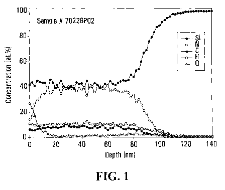
(Table 5) and Elastic Recoil Detection (ERD) (Figures 1-3).
28
CA 02670809 2009-07-17
WO 2008/104059 PCT/CA2008/000357
Table 4: Deposition conditions used to prepare exemplary
films.
Sample Name 70208P02 70226P01 70226P02 70312P01A
Coated films a-SiCN a-SiCN a-SiCN a-SiCN
Lifetime ( s) 1121.7 to 1488.7 1962.2 843.52
1657.5
Substrate type FZ Si (100) FZ Si (100) FZ Si (100) FZ Si (100)
Resistivity 3.5-10 3.5-10 3.5-10 3.5-10
(KS2)
Temperature C 400 400 400 400
PDMS flow 35 35 35 35
(sccm)
Argon (sccm) 100 100 100 100
NH3 flow 75 250 250 250
(sccm)
Reactor power 900 900 900 900
(Watt)
Chamber 258 335 330 298
pressure
(mTorr)
Table 5: XPS structural analysis of exemplary a-SiCN:H
films.
Samples %at.Si %at.C %at.O %at.N Lifetime ( s)
70208p02 48.0 14.0 3.0 35.0 1121
70226p02 47.4 14.6 1.5 36.5 1962
70312p01A 35.3 16.5 8.5 39.7 844
70312p01B 47.5 16.4 1.6 34.5 422
Two techniques were used to evaluate the effective lifetime
of the minority carriers in the exemplary films: (1)
microwave photoconductive decay ( -PCD) developed by SEMILAB
Semiconductor Physics Laboratory, Inc., and (2) Quasi-
Steady-State photo conductance (QSSPC) using a WCT-120
instrument developed by Sinton Consulting, Inc. The results
of the two techniques were found to be comparable within 5%
29
CA 02670809 2009-07-17
WO 2008/104059 PCT/CA2008/000357
by measuring a sample with each technique (Figures 4, 5(a)
and 5 (b) ) .
Lifetimes of up to 2500 s on SiCN:H passivated 4" FZ Si
(100) wafers were measured using the QSSPC method (Figure
4). Lifetimes of the passivating films produced by the
method described herein are unexpectedly better than those
found in the art (see Table 6).
Table 6.
Passivation Substrate Resistivity Seff Effective Ref.
films FZ Si ~ cm cm.s-1 life time
( s)
PE-CVD a-SiC N 1.5 100 12
PE-CVD a-SiCN N 1.5 2-3
PE-CVD a-SiC 1.4-1.6 54 100 13
PE-CVD a-SiCN 16 1000
PE-CVD a-SiC N 0.85 <100 14
Native oxide N 1 130 15
1 10-20
50 2020
50 215
50 470
50 195
PE-CVD a-SiC P 3.3 30 585 16
0.4 2400 8
0.4 650 33
PE-CVD a-SiC P 1 1300 <5 17
PE-CVD a-SiC P 3.3 29 ----- 18
N 1.4 50 -----
PE-CVD a-SiC P 3-4 30 ------ 19
PE-CVD a-SiC(n) 10 ------
PE-CVD a-SiC(n) P 1 953 20
PE-CVD a-SiC 1356 21
From the above results, it can be seen that addition of NH3
in the gas flow leads to an increase in the measured
lifetime for the a-SiC:H passivated 4" FZ Si (100) wafers,
demonstrating that the passivation effect can be varied by
the presence of nitrogen and/or hydrogen atoms(i.e. the
saturation of free bonds).
CA 02670809 2009-07-17
WO 2008/104059 PCT/CA2008/000357
Although the foregoing invention has been described in some
detail by way of illustration and example for purposes of
clarity of understanding, it is readily apparent to those of
ordinary skill in the art in light of the teachings of this
invention that certain changes and modifications may be made
thereto without departing from the spirit or scope of the
appended claims.
The citation of any publication, patent or patent
application in this specification is not an admission that
the publication, patent or patent application is prior art.
It must be noted that as used in the specification and the
appended claims, the singular forms of "a", "an" and "the"
include plural reference unless the context clearly
indicates otherwise.
Unless defined otherwise all technical and scientific terms
used herein have the same meaning as commonly understood to
one of ordinary skill in the art to which this invention
belongs.
31
CA 02670809 2009-07-17
WO 2008/104059 PCT/CA2008/000357
REFERENCES
1. Yao, U.S. Patent No. 5,800,878.
2. Gardiner et al., U.S. Patent No. 5,820,664.
3. Chayka, U.S. Patent No. 5,952,046.
4. M.W. Pitcher et al., Advanced Mater., 16(8), 706 (2004).
5. Goldstein, U.S. Patent No. 5,850,064 and Shen et al.,
U.S. Patent No. 6,730,802.
6. Goela et al., U.S. Patent No. 5,612,132.
7. Moehle et al., U.S. Patent No. 5,209,979.
8. Ruppel et al., U.S. Patent No. 5,944,963.
9. M.S. Aida and M. Ghrieb, Mater. Chem. and Phys., 47(1),
97-100 (1997).
10. R. Riedel, A Kienzle, W. Dressler, L. Ruwisch, J. Bill,
and F. Aldinger, Nature, 382, 796 (1996).
11. P.A. Ramakrishnan, Y.T. Wang, D. Balzar, Linan An, C.
Haluschka and R. Riedel, and A.M. Hermann, Appl. Phys.
Lett., 78(20), 3076 (2001).
12. M. Vetter, I. Martin, A. Orpella, J. Puigdollers, C.
Voz, R. Alcubilla, Thin solid Films, 451-452 (2004)
pp. 340-344.
13. I. Martin, M. Vetter, A. Orpella, C. Voz, J.
Puigdollers, and R. Alcubilla, Appl. Phys. Lett. 81 (23)
(2002) 4461-4463.
14. M. Vetter, C. Voz, R. Ferre, I. Martin, A. Orpella, J.
Puigdollers, J. Andreu, and R. Alcubilla, Thin Solid Films,
511-512 (2006) 290-294.
32
CA 02670809 2009-07-17
WO 2008/104059 PCT/CA2008/000357
15. A. Cuevas, Solar energy Mater. Sol. Cells, 71 (2002)
pp. 295-312.
16. I. Martin, M. Vetter, A. Orpella, and J. Puigdollers,
A. Cuevas, R. Alcubilla, Appl. Phys. Lett., 79 (14), (2001)
pp. 2199-2201.
17. S. W. Glunz, Presented at the 4th World Conference on
Photovoltaic Energy Conversion, Hawaii, May 2006.
18. I. Martin, M. Vetter, M. Garin, A. Orpella, C. Voz,
J. Puigdollers, and R. Alcubilla J. Appl. Phys., 98 (2005)
pp. 114912.
19. M. Vetter, I. Martin, A. Orpella, C. Voz, J.
Puigdollers and R. AlcubillaMat. Res. Soc. Symp. Proc., 715
(2002) pp. A24.5.1.
20. S. Janz, S. Riepe, M. Hofmann, S. Reber, and S. Glunz,
Appl. Phys. Lett., 88 (2006) pp. 133516.
21. S. W. Glunz, S. Janz, M. Hofmann, T. Roth, and
G. Willeke, Paper presented at the 4th World Conference on
Photovoltaic Energy Conversion, Hawaii, May, 2006.
33