Note: Descriptions are shown in the official language in which they were submitted.
CA 02671163 2009-05-29
WO 2008/068387 PCT/F12007/050667
1
An electric sensor web, system and a method for its manufacture
FIELD OF INVENTION
The present invention relates to a sensor web. The sensor web can be
used for example in floor constructions for monitoring electrically
conductive objects, objects with dielectric properties and objects
containing charges, for example the movement and location of a
human body as described for example in publication
W02005/020171A1. For example, the sensor web is useful for
monitoring aged and disabled people and their vital functions. Other
possible applications are monitoring of inmates in jails and prisons,
home and industrial automation applications, vehicle airbag systems
and other sensing applications.
The present invention also relates to a method for manufacturing of a
sensor web.
BACKGROUND
Publication WO 2006/003245 discloses a sensor product for electric
field sensing. The sensor product is in web form, and it comprises
sequential conductive areas which have been connected to
conductors. The conductors are parallel to each other.
Publication WO 2006/003245 discloses that parallel straight conductors
extend in the longitudinal direction of a web. The publication teaches
that there are two possibilities to arrange the contact between a
conductive area and a conductor: 1) a via is formed through the web,
and it is filled with conductive ink while the conductor is formed e.g. by
printing on the reverse surface of the web, thus forming a conductive
path through the web, 2) a dielectric bridge is formed over the
CA 02671163 2009-05-29
WO 2008/068387 PCT/F12007/050667
2
conductors, and the dielectric bridge is discontinuous at the point
where an electric contact is desired.
In order to achieve an easy to use and functional sensor web, the
construction of the contact between the conductive area and the
conductor is highly important because the web should be cuttable
wherever desired.
SUMMARY OF THE INVENTION
The aim of the invention is to create a sensor web which has a simple
structure and is easy to manufacture. When the sensor web, i.e. the
conductive sensor area, is implemented in one plane or layer, no vias
or dielectric bridges are required.
An additional benefit of the structure among some variations of the
sensor web is that the patterning of the sensor electrodes and
conductors can be done in simple processing steps, even as a single
processing step..
Furthermore, the sensor structure presented here can also be
characterized by the feature that the sensor web can be cut across the
longitudinal direction of the web anywhere along this direction, and the
cutoff sensor laminate will form a functional entity up to the sensor
count that does not exceed the number of conductors crossing the
cutting edges. Thus, during manufacturing, the structure of the sensor
web is insensitive to the number of the conductive areas which are
required in a specific sensor web for a given application or system to
be assembled.
The sensor web comprises a substrate having a longitudinal direction,
successive electrically conductive areas on the surface of the substrate
CA 02671163 2015-04-10
3
and a group of parallel conductors (i.e. conductors next to each other) which
advance in the longitudinal direction of the substrate. The electrically
conductive
areas act as capacitive sensors, which are connected to suitable electronics
via the
conductors. The sensor web can be manufactured by using a roll-to-roll process
or -
tools or any other mass production process that can take use of the
identically
repetitive pattern of the sensor areas in the web direction.
According to embodiments of a first aspect of the invention, there is provided
a
sensor web for electric field sensing, comprising: a substrate having a
longitudinal
direction, at least one array of electrically conductive sensor areas formed
on a
surface of the substrate in the longitudinal direction of the substrate, a
group of
parallel conductors formed on the surface of the substrate, each electrically
conductive sensor area being electrically connected to one conductor, wherein
the
parallel conductors are spaced from each other and arranged in a sidestep
manner
in the longitudinal direction of the substrate, wherein the conductors formed
on the
substrate provide space for subsequently added conductors, wherein the
substrate
is adapted to be cut between any two electrically conductive sensor areas to
make
functional sensor arrays.
zo According to embodiments of a second aspect of the invention, there is
provided a
method for manufacturing of a sensor web, the method comprising: die-cutting a
metal foil attached to a surface of a release web to form electrically
conductive areas
and conductors electrically connected to the electrically conductive areas,
wherein
the conductors are formed parallel to each other, spaced from each other and
in a
sidestep manner such that conductors are adapted to be added one by one to the
group of conductors advancing in the longitudinal direction of the substrate,
wherein
conductors formed on the substrate provide space for subsequently added
conductors, wherein the substrate is adapted to be cut between any two
electrically
conductive sensor areas to make functional sensor arrays, attaching a first
protective film to the release web so that the first protective film covers
the
CA 02671163 2015-04-10
,
,
3a
electrically conductive areas and conductors, and replacing the release web
with a
backing film.
According to embodiments of a third aspect of the invention, there is provided
a
system for monitoring a space, the system comprising: at least one length from
a
sensor web comprising a substrate having a longitudinal direction, at least
one array
of electrically conductive sensor areas formed one after another spaced apart
from
each other in a successive manner along the longitudinal direction and
arranged on
one side of the substrate, and a group of parallel conductors formed on the
same
lo side of the substrate, each electrically conductive sensor area
being electrically
connected to one conductor, wherein the parallel conductors are spaced from
each
other and arranged in a sidestep manner in the longitudinal direction of the
substrate, wherein the conductors formed on the substrate provide space for
subsequently added conductors, wherein the substrate is adapted to be cut
between
any two electrically conductive sensor areas to make functional sensor arrays,
each
electrically conductive area that is to be used for sensing purposes being
electrically
connected to one conductor, and a detector configured to detect an output
signal
from at least one electrically conductive area.
The substrates may be in a web form. The substrate typically comprises plastic
material, or fibrous material in the form of a nonwoven fabric, fabric, paper,
or board.
Suitable plastics are, for example, plastics comprising polyethylene
terephtalate
(PET), polypropylene (PP), or polyethylene (PE). The substrate is preferably
substantially flexible in order to conform with other surfaces on which it is
placed.
Besides one layer structure, the substrate can comprise more layers attached
to
each other. The substrate may comprise layers that are laminated to each
other,
extruded layers, coated or printed layers, or mixtures of these. Usually,
there is a
protective layer on the surface of the substrate so that the protective layer
covers the
electrically conductive areas and the conductors. The protective layer may
consist
of any flexible material, for example paper, board, or plastic, such as PET,
PP, or
CA 02671163 2015-04-10
,
3b
PE. The protective layer may be in the form of a nonwoven, a fabric, or a
foil. A
protective dielectric coating, for example an acrylic based coating, is
possible.
The electrically conductive areas comprise electrically conductive material,
and the
electrically conductive areas can be, for example, but are not limited to,
printed
layers, coated layers, evaporated layers, electrodeposited layers, sputtered
layers,
laminated foils, etched layers, foils or fibrous layers. The electrically
conductive area
may comprise conductive carbon, metallic layers, metallic particles, or
fibers, or
electrically conductive polymers, such as polyacetylene, polyaniline, or
polypyrrole.
Metals that are used for forming the electrically conductive areas include for
example aluminum, copper
CA 02671163 2009-05-29
WO 2008/068387 PCT/F12007/050667
4
and silver. Electrically conductive carbon may be mixed in a medium in
order to manufacture an ink or a coating. When a transparent sensor
product is desired, electrically conductive materials, such as ITO
(indium tin oxide), PEDOT (poly-(3,4-ethylenedioxythiophene)), or
carbon nanotubes, can be used. For example, carbon nanotubes can
be used in coatings which comprise the nanotubes and polymers. The
same electrically conductive materials also apply to the conductors.
Suitable techniques for forming the electrically conductive areas
include, for example, etching or screen printing (flat bed or rotation),
gravure, offset, flexography, inkjet printing, electrostatography,
electroplating, and chemical plating.
Besides the above-mentioned methods for manufacturing the web, the
following manufacturing method may be used. A metal foil, such as an
aluminum foil, is laminated on a release web. The electrically
conductive areas and the conductors are die-cut off the metal foil, and
the remaining waste matrix is wound onto a roll. After that, a first
protective film is laminated on the electrically conductive areas and the
conductors. Next, the release web is removed and a backing film is
laminated to replace the release web.
Benefits of the above-mentioned manufacturing method include:
- the raw material is cheaper,
- the manufacturing method is cheaper compared to e.g. etching,
- the manufacturing method requires only one production line, and
- the resulting sensor web is thinner; the thickness of the sensor web
may be less than 50 pm.
The above-mentioned manufacturing method may also be applied to
such sensor webs which comprise sequential electrically conductive
areas and a group of conductors which extend in the longitudinal
direction of the web. Such a sensor web is known from WO
2006/003245. The electrically conductive areas and the group of
conductors are die-cut from a metal foil, and they are laminated
between two substrates, i.e. between two superimposed webs. In order
to couple an electrically conductive area to a conductor, an electrically
CA 02671163 2009-05-29
WO 2008/068387 PCT/F12007/050667
conductive bridge between them is necessary. Because the substrate
is an electric insulator, vias through the substrate are required. The
vias through one of the substrates are arranged, for example, by
drilling or by perforating the substrate. Next, the vias are filled with
5 electrically conductive ink during printing of electrically conductive
bridges.
Furthermore, the manufacturing method may be applied to such sensor
webs which comprise two or more superimposed layers. For example,
electrically conductive areas and their conductors may be located in
one layer, and optional RF loops and their conductors may be located
in another layer. In principle, it is possible to use different techniques,
e.g. etching, printing, or die-cutting, in the same product. For example,
the electrically conductive areas may be die-cut from a metal foil, but
their conductors may be etched on a substrate. The electrically
conductive areas and their conductors are connected to each other
through vias.
The sensor web is provided with an output in order to make it possible
to connect the output to the control electronics. For example,
measurement voltages and control output currents can be fed through
the output. For a person skilled in the art it is clear that the nature of
output signals can vary according to the application. For example, in
the case of capacitive measurements, no effective current signal is
available. In practice, the output can comprise conductors next to each
other without any connector. In other words, the output is formed by
cutting the sensor web across its longitudinal direction to a desired
length, and thus the ends of the conductors are exposed and are ready
for forming an electrical contact. The attachment method of the sensor
web in contact can be, but is not limited to, crimp connector, spring
connector, welded contact, soldered contact, isotropic or anisotropic
adhesive contact. However, a standard connector used in common
electronic applications (e.g. Crimpflex0, Nicomatic SA, France) can be
added to the output.
CA 02671163 2009-05-29
WO 2008/068387 PCT/F12007/050667
6
Each electrically conductive area to be used for sensing is connected
to a conductor which forms an electrically conductive path between the
electrically conductive areas and the output. The conductors form a
group of parallel conductors which each of them is adapted to join.
When one conductor joins the group, each of the other conductors of
the group gives space for the joining conductor so that the conductors
do not cross each other. The group of conductors advance in the
longitudinal direction of the substrate.
The above-mentioned principle can be implemented in different ways.
For example, the parallel conductors may extend diagonally on the
substrate, or the parallel conductors may sidestep when a new
conductor joins the group of conductors.
The conductor may comprise only one part, i.e. the first part, or it may
comprise two parts, i.e. the first and second parts. For example, the
conductor may be straight throughout its length, thus consisting of only
the first part, or the conductor may be formed of two straight parts
which are connected to each other so that the parts form an angle to
each other. It is also possible that the part which is in a physical
contact with the conductive area, i.e. the second part, is curved. One
possible option is that the first parts extend, for example, as waves but
they have a certain linear advancing direction. Further, the conductors
may wind according to a predetermined pattern so that their distance
from each other is constant, i.e. the conductors are parallel despite the
winding. In that case, the advancing direction is determined by
connecting the starting point of the conductor, or the starting point of
the first part of the conductor, to the end point (the output) of the
conductor with a straight line. The straight line illustrates the advancing
direction. However, the basic principle, i.e. that each of the other
conductors of the group gives space for the joining conductor so that
the conductors do not cross each other, is realized as well.
In certain embodiments of the invention, the conductors may be
arranged in a widened manner in some positions of the web in order to
ease the connections using a connector. Between such widened
CA 02671163 2009-05-29
WO 2008/068387 PCT/F12007/050667
7
positions the conductors travel in the longitudinal direction of the web in
an arrangement that is as narrow as possible to save space for the
sensor area.
The first parts of the conductors may form an angle with the
longitudinal direction of the substrate. The absolute value of the angle
is greater than 0 but smaller than 90 , typically greater than 0.01 but
smaller than 30 , more typically greater than 0.1 but smaller than 5 .
Instead of being smaller than 5 , the upper limit may be smaller than
3 . Very useful ranges are that the absolute value of the angle is
greater than 0.5 but smaller than 1.5 , or that the absolute value of the
angle is greater than 0.2 but smaller than 2 . When the first parts
extend, for example, as waves, the linear advancing direction of the
first parts of the conductors form an angle with the longitudinal direction
of the substrate. Similarly, when the straight line illustrates the
advancing direction of the freely winding or curling conductor, the
straight line forms an angle with the longitudinal direction of the web.
One possible way to implement the conductors is to arrange the group
of the parallel conductors so that the other members of the group
sidestep when a new conductor joins the group of parallel conductors.
For example, the conductors may comprise a pattern which consists of
a diagonal part and a part which is joined to the diagonal part and
extends in the longitudinal direction of the web. The first diagonal part
begins from the electrically conductive area. The pattern is repeated
one after another so that the conductor is transferred in the cross-
direction of the web.
A conductor structure, which is almost similar to the above-mentioned
lay-out, may comprise a part which extends in the longitudinal direction
of the sensor web and a part which is transverse to the first mentioned
part. The parts form a step-shaped pattern which is able to sidestep
when a new conductor joins the group of the conductors.
CA 02671163 2009-05-29
WO 2008/068387 PCT/F12007/050667
8
The purpose of the above-mentioned arrangement for conductors is to
bring electrical leads from the conductive areas to the edge of web so
that a) the conductors do not cross each other, and b) the conductors
at the edge of web are equally spaced from each other. This
arrangement provides a constant cross directional distance between
the conductors extending from the conductive areas that are located in
different positions in the web direction. Thus, no vias or dielectric
bridges are required when the sensor web is implemented in one plane
because the conductors can extend without crossing or disturbing each
other. Such an arrangement provides an easy and reliable connection
between the series of conductive areas and corresponding series of
the conductors at the edge of the web with a constant distance
between connectors. Furthermore, the web can be cut wherever
desired and the order of the conductors in the cutting position
corresponds in a known manner to the positions of the sensor areas in
the sensor array as defined by their distance from the cutting position.
The sensor web comprises repetitive patterns which comprise
successive and/or sequential conductive areas and their conductors.
For example, one pattern may be formed from five successive
conductive areas and their conductors. The above-mentioned pattern is
repetitive over the length of the web.
The number of successive electrically conductive areas 1 to N in the
web is defined by the total number of conductor lines arranged to run
along the web direction. Typically, the number of conductors is kept
constant along the web, which means that when a new conductor is
adapted to join the group of successive conductors and the other
conductors in this group are adapted to give space for this joining
conductor, then the run of the outermost conductor on the other side of
this group is terminated. Thus, the total repetitive pattern of the
successive conductive areas is defined by the total number of parallel
conductor lines. This number can be freely chosen according to a given
application.
CA 02671163 2009-05-29
WO 2008/068387 PCT/F12007/050667
9
Besides the above-mentioned elements of the sensor web, the sensor
web may include, for example, RF loops and their conductors. They
may also be made of a metal foil. The RF loops and their conductors
may be arranged in the same layer as the electrically conductive areas
and their conductors, or the RF loops and their conductors and the
electrically conductive areas and their conductors may be arranged in
superimposed layers.
The sensor web may also include a continuous secondary sensor
element whose parts intermesh with the electrically conductive areas.
The continuous secondary sensor element can be reserved for a
common signal, such as a ground signal. This kind of a solution is
important for reducing the electrical noise level and thus for increasing
the sensitivity of the measurement.
Further, the sensor web may comprise several arrays of successive
electrically conductive areas. The electrically conductive areas do not
need to be aligned in the cross direction of the web. The shape of the
electrically conductive areas can be circles, squares but also any other
shapes are feasible. As a skilled person will readily understand, the
electrically conductive areas may have almost any imaginable shape.
However, some shapes may be more beneficial than others e.g. in
regard to their distribution over the sensor web and thus to the
positional sensing capability of the web.
The present invention also relates to a system for monitoring a space.
The space may be, for example, a single room or a group of rooms to
be monitored. The system comprises a given length cut from the
sensor web described in this application Thus, the length also
comprises a substrate having a longitudinal direction, at least one
array of successive electrically conductive areas formed on the surface
of the substrate, and a group of conductors formed on the surface of
the substrate. Each active electrically conductive area is electrically
connected to one conductor. The conductors are adapted to join one
by one the group of the conductors advancing in the longitudinal
CA 02671163 2009-05-29
WO 2008/068387 PCT/F12007/050667
direction of the substrate, and the other conductors of the group are
adapted to give space for the joining conductor. When a new conductor
joins the group on one side of the group, another conductor ends
approximately at the same location on the other side of the group. The
5 length is usually mounted on a floor under the wearing surface of the
floor. The system also comprises means for sending an input signal to
at least one electrically conductive area and means for detecting an
output signal from at least one electrically conductive area. The output
signal may be, for example, a differential signal or a sum signal in
10 addition to a single-ended signal. In a passively operating sensor
system, the input signal may not be required.
BRIEF DESCRIPTION OF THE FIGURES
In the appended figures,
Figs. 1 to 4 show the top views of sensor webs for monitoring
conductive objects,
Fig. 5 shows a cross-sectional view (section A-A in Fig. 1) of the
sensor web of Figs. 1 to 4,
Figs. 6 to 9 show the top views of sensor webs for monitoring
conductive objects,
Fig. 10 shows a schematic view of a manufacturing method,
Fig. 11 shows one possible way of manufacturing RF loops,
Fig. 12 shows a layer of a two-layered product,
Fig. 13 shows a top view of a two-layered product,
Fig. 14 shows a cross sectional view of a two-layered product (section
B-B in Fig. 13),
CA 02671163 2015-04-10
11
Fig. 15 shows one possible lay-out of a product comprising electrically
conductive
areas and RF loops,
Figs. 16 and 17 show top views of sensor webs for monitoring conductive
objects,
and
Fig. 18 shows a magnified view of specifics of Fig. 17.
DETAILED DESCRIPTION
Fig.1 illustrates a sensor web W for monitoring electrically conductive
objects, for
example the movement and location of a human body. It is possible, for
example, to
use the web W for monitoring aged and disabled people. Also, possible
applications
include but are not limited to monitoring of jails and prisons, home and
industrial
automation, vehicle airbag systems and other sensing applications. The sensor
web
W comprises successive electrically conductive areas 1. A conductor 2 connects
the electrically conductive area 1 to an output 3. The output 3 is provided
with a
connector. The parallel conductors 2 extend linearly and form an angle a to
the
longitudinal direction LD of the web W.
Fig. 2 shows another possible lay-out of a sensor web W. The web W comprises
two rows of successive electrically conductive areas 1. Conductors 2, which
connect the electrically conductive areas 1 on the upper row to an output 3 on
the
left hand side, are parallel to conductors 2, which connect the electrically
conductive
areas 1 on the lower row to an output 3 on the right hand side. The parallel
conductors 2 extend linearly and form an angle to the longitudinal direction
LD of the
web W.
Fig. 3 shows yet another possible lay-out of a sensor web W. The web W
comprises
two rows of successive electrically conductive areas 1 and conductors 2 which
connect the electrically conductive areas to an output 3. The electrically
conductive
areas 1 on the upper row and their conductors 2 and the electrically
conductive
areas 1 on the lower row and their conductors 2 form a mirror image. The
conductors of the
CA 02671163 2009-05-29
WO 2008/068387 PCT/F12007/050667
12
upper row are parallel to each other and so are the conductors of the
lower row.
Fig. 4 further shows one possible lay-out of the sensor web W.
Conductors 2 comprise first parts 2a which extend linearly, and they
form an angle with the longitudinal direction LD of the web W. The
conductors 2 may comprise second parts 2b which are transverse to
the longitudinal direction of the sensor web W. However, the shape of
the second part may vary.
Fig. 5 shows a cross-sectional view (section A-A). The sensor product
comprises a substrate 5, electrically conductive areas 1 which form
sensor elements formed on the surface of the substrate 5 and
conductors 2 connecting the sensor elements to an output 3. The
electrically conductive areas 1 may, for example, consist of etched
copper. On top of the substrate 5 there is a protecting layer 4.
Fig. 6 shows a possible lay-out of the sensor web W. In this case, the
junction of the first part 2a and the second part 2b is curved.
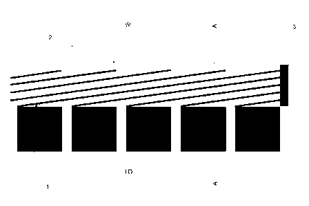
Fig. 7 shows another possible lay-out of the sensor web W. A
conductor pattern consists of a part 6a and a part 6b. The part 6a is
diagonal, and the part 6b extends in the longitudinal direction of the
web W. The conductor pattern is repeated so that the whole conductor
2 is formed. When a new conductor 2 joins the group of the
conductors, the other conductors 2 of the group are adapted to give
space for the new conductor 2, i.e. the other conductors are adapted to
sidestep.
Fig. 8 shows a lay-out realized by using conductors 2 consisting of a
part 6a which is parallel to the cross direction of the web W and a part
6b which extends in the longitudinal direction of the web W. Thus, the
parts 6a, 6b are perpendicular to each other. When a new conductor 2
joins the group of the conductors, the other conductors 2 of the group
are adapted to give space for the new conductor 2, i.e. the other
conductors are adapted to sidestep.
CA 02671163 2009-05-29
WO 2008/068387 PCT/F12007/050667
13
Fig. 9 shows still another possible lay-out of the sensor web W. There
are two sequential arrays of conductive areas 1. Each conductive area
1 is in connection with a conductor 2. The conductors 2 comprise a first
part 2a and a second part 2b or 2b'. The first parts 2a of the conductors
2 form an angle with the longitudinal direction of the substrate.
Fig. 10 shows a schematic view of a possible manufacturing method. A
release web 8 is unwound from a roll 7. Hotmelt adhesive is applied on
the release web 8 in a coating nip 9. After its application, the hotmelt
adhesive is cooled; for the cooling, a cooling roll 10 may be used. A
metal foil 12, such as an aluminium foil whose thickness may be from 5
pm to 20 pm, for example, is unwound from a roll 11. The metal foil 12
and the release web 8 are laminated together in a laminator nip 13.
Next, the metal foil 12 is die-cut in a rotary die-cutter 14 in order to form
the conductive areas 1 and the conductors 2, but the release web 8
remains solid. The waste matrix that is not used for the product is
wound onto a roll 15.
A first protective film 16, i.e. the protective film with adhesive for the
face side of the web W, is unwound from a roll 17. The protective film
16 has been provided with a release web 18 which is wound onto a roll
19. The release web 8 having the conductive areas 1 and the
conductors 2 on its surface is laminated with the protective film 16 in a
laminator nip 20. After that, the release web 8 is removed and wound
onto a roll 21.
It is important that the first protective film 16 is immediately laminated
onto the release web 8 because otherwise the conductive areas 1 and
the conductors 2 made of the metal foil could be wrinkled or be
otherwise damaged. They are also poorly adhered to the release web
8. Immediately means in this case that no such a process step can
take place between the die-cutting step and the laminating step which
could wrinkle or otherwise damage the items which are die-cut from the
metal foil, i.e. there should not be e.g. any sharply turning angles or
rolls having a small diameter on the production line.
CA 02671163 2015-04-10
14
A backing film 24, i.e. the protective film with adhesive for the reverse side
of the
web W, is unwound from a roll 22. The backing film 24 has been provided with a
release web 25 which is wound onto a roll 23. The backing film 24 is laminated
in a
nip 26 with the first protective film 16 so that the electrically conductive
areas 1 and
the conductors 2 remain between the two protective films 16, 24. After the nip
26,
the sensor web is wound onto a roll 27. Backing film may also be applied
without
adhesive and release web since there is already adhesive on the first
protective film
16 and on the conductive areas.
3.0 The above-mentioned method can be used for the sensor webs which are
described
above and in the examples below in this application. Further, the method can
be
utilized in such sensor webs as described in WO 2006/003245 which discloses
parallel straight conductors extending in the longitudinal direction of a web.
A via
may be drilled through the first or the second protective film (i.e. the
backing film),
and the via is filled with conductive ink, thus forming a conductive path
through the
web. It is also possible that the first protective film or the backing film is
perforated.
Fig. 11 shows one possible way of manufacturing RF loops 28. The RF loops 28
and their conductors 29 are die-cut from a metal foil in a process which is
similar to
that process which is shown for the electrically conductive areas 1 and their
conductors 2 in Fig. 10.
Fig. 12 shows the first layer of a two-layered sensor web W2. The first layer
comprises a substrate, electrically conductive areas 1 and their conductors 2.
Fig. 13 shows a two-layered sensor web W2. The sensor web W2 is illustrated as
being transparent so that the first layer can be seen trough the second layer.
The
first layer is as illustrated in Fig. 12, i.e. the first layer comprises
electrically
conductive areas 1 and their
CA 02671163 2009-05-29
WO 2008/068387 PCT/F12007/050667
conductors 2. The second layer is as illustrated in Fig. 11, i.e. the
second layer comprises RF-loops 28 and their conductors 29.
Fig. 14 shows a cross-sectional view of the sensor web of Fig. 13
5 (section B ¨ B). The sensor web comprises two layers, the first layer 30
and the second layer 31 which are attached to each other. The layers
may be attached by using e.g. adhesive. The first layer 30 comprises
RF loops 28 and their conductors 29. The second layer 31 comprises
electrically conductive areas 1 and their conductors 2. The first layer 30
10 may be covered by a third layer 32. The first layer 30 and the third
layer 32 may be adhesively attached to each other. It is possible to
connect the conductors of both layers 30, 31 to the same connector by
using a crimp connector which partially breaks the structure of the
sensor web at the connector.
The two-layered web may be manufactured so that both of the layers
are manufactured separately, i.e. the electrically conductive areas and
their conductors on one release web are attached to one protective
film, and the RF loops and their conductors on another release web are
attached to another protective film. One of the release webs is
removed, and the protective films are laminated together. A backing
film is attached to cover those elements which remain exposed, i.e.
either the electrically conductive areas and their conductors, or the RF
loops and their conductors.
Fig. 15 shows a top view of a sensor web W comprising electrically
conductive areas 1, conductors 2 of the electrically conductive areas,
RF loops 28 and conductors 29 of the RF loops. When the conductors
2 of the electrically conductive areas 1 and the conductors 29 of the RF
loops 28 intermesh, as shown in Fig. 15, it is possible to arrange all the
required elements, i.e. the electrically conductive areas 1, the RF loops
28 and the conductors 2, 29, to only one layer.
Figs. 16 and 17 show top views of a sensor web W. A common feature
in these drawings is that the area which has been reserved for
conductors 2 is made very narrow compared to the whole width of the
CA 02671163 2009-05-29
WO 2008/068387 PCT/F12007/050667
16
area on which both conductive areas 1 and conductors 2 exist. The
width of the area which has been reserved for the conductors 1 might
be 15 `)/0, preferably 10 `)/0, of the total width of the area on which the
conductive areas 1 and the conductors 2 are situated. The reason for
this arrangement is that the conductive areas 1 should have as much
space as possible reserved for sensing use. The conductive areas 1
and the conductors 2 are situated on the same side of the web. The
webs of Figs. 16 and 17 are also provided with a continuous secondary
sensor element 40 which has been reserved for a common signal, such
as a ground signal. The ground signal and the shape of the conductive
areas 1 can be used to have an effect on the noise level of the signals
and thus, for enhancing the sensitivity of the sensors. The use of the
ground signal is not obligatory but may be used in applications
requiring sensitivity and less electrical noise.
Depending on the application, the ground signal or other common
signal may skip some of the electrically conductive areas 1, and may
instead be arranged to only every second up to every nth conductive
area 1, for example.
In the embodiment illustrated in Fig. 9, for example, the conductive
areas 1, arranged side by side and forming, in principle, sensor area
pairs, can be used in such a manner that the first one of the sensor
areas in such a pair can be used as a ground signal against which the
signal from the second area in that same pair can be measured.
Further, the ground signal areas in different pairs can be connected
together into a common ground level or they can be kept separate.
In the embodiment illustrated in Fig. 1, for example, each of the
conductive areas 1 can be encircled with guard rings providing a
secondary sensor element to be used, for example, as a ground signal.
Such guard rings may enclose the conductive area from all directions
except leaving a route for the conductor 2b. Again, such guard rings
may all be connected together to provide a common secondary
sensor/signal or they can be kept separate, for example, for differential
measurement purposes.
CA 02671163 2009-05-29
WO 2008/068387 PCT/F12007/050667
17
In Fig. 16, the conductive areas 1 and the continuous secondary
sensor element 40 form a pattern which resembles crossing fingers,
i.e. the conductive areas 1 have the shape of the letter "E" and the
continuous secondary sensor element 40 has a part which resembles
the mirror image of the letter "E", and the shape of the letter "E" and its
mirror image intermesh.
In Fig. 17, the pattern follows the same principle as in Fig. 16 but the
conductive areas 1 and the continuous secondary sensor element have
been accomplished by circular shapes connected with narrow
conductors.
In order to simplify the electrical connection to the sensor web, the
group of conductors 2 has been widened in the cross web direction in
locations A and B as shown in Figs 16 and 17 to adapt more readily to
a connector or another connection arrangement. The web is preferably
cut at these locations so that the connector can be simply arranged at
the edge of the web. Naturally, the other end of the web for any given
length can be cut anywhere along the web direction without affecting
the functionality of the sensors.
When the web is cut at a desired location (for example connector
locations A or B), the mutual order of the conductors 2 with respect to
the location of an electrically conductive area 1 as defined from the
cutting location, i.e. the connector location, is known. For example, in
cutting/connector location A (see Figs 16 and 17), the 1st conductor is
always the common signal (ground), the 2nd conductor is the closest
sensor (sensor 1) as counted from the cutting location. For location B,
again the 1st conductor is the common signal, the 2nd conductor is the
closest sensor (sensor 2) from the cutting location and the 3rd
conductor is the next sensor (sensor 1).
Fig. 18 shows a magnified view of specifics of Fig. 17. Fig. 18
illustrates how the group of conductors have been widened and how a
conductor 2 joins a group of conductors.
CA 02671163 2009-05-29
WO 2008/068387 PCT/F12007/050667
18
Throughout this application, the term "successive" is used when
describing the mutual positioning of the sensor areas within an array
consisting of such sensor areas. These arrays again will follow each
other in a repetitive manner along the longitudinal direction of the web.
Successive sensor areas are not limited here to embodiments where
such areas follow each other along the longitudinal direction so that the
area of the previous sensor needs to end in the longitudinal direction
before the area of the successive sensor begins. It is also possible that
these two or more sensor areas "overlap" each other in the cross web
direction so that both sensors run side-by-side for a certain length of
the web. All embodiments that are arranged to have galvanically
separated sensor areas provided along the longitudinal direction of the
web in some manner where this patterning advances along said
longitudinal direction, are possible. The sensor areas within an array
do not need to form any specific sequence.
In the following, the invention will be described by examples:
EXAMPLE 1.
A sensor web according to the invention is manufactured. The metal
parts can be made of, for example, etched aluminium or copper, and
the polymer parts of, for example, PET, PP or PE.
Manufacturing steps:
1. Patterns of continuous conductor lines and conductive sensor areas
are first printed, for example, on the copper/PET or aluminum/PET
laminate with an UV etch resist (e.g. Coates XV1000).
2. The metal outside the resist area is removed by etching. (After that,
also the resist layer may be removed.)
3. Protective layers are coated or laminated (e.g. PET, PP or PE-film)
4. Connector and/or electronics is attached
CA 02671163 2009-05-29
WO 2008/068387 PCT/F12007/050667
19
The resist printing can be made by any common printing technique, for
example by screen printing (flat bed or rotation), gravure, offset, or
flexography.
The etching can be made by any common etching process, for
example a process based on ferric chloride, sodium hydroxide, or
hydrogen chloride.
EXAMPLE 2.
Conductive areas include, for example, conductive silver or carbon,
and polymer parts consist of PET, PP or PE.
1. Continuous conductor lines and conductive sensor areas are printed
with conductive paste (e.g. silver or carbon paste) onto the substrate
2. Protective layers are coated or laminated (e.g. PET, PP or PE-film)
3. Connector and/or electronics is attached
Conductors and sensors can be printed by any common printing
technique, such as, for example screen printing (flat bed or rotation),
gravure, offset or flexography.
EXAMPLE 3.
1. Continuous conductor lines and conductive sensor areas are die-cut,
for example, from copper/PET or aluminum/PET laminate
2. Protective layers are coated or laminated (e.g. PET, PP or PE-film)
3. Connector and/or electronics is attached
A skilled person will readily understand that all the features of the
sensor web are interchangeable. If a certain feature is explained in
connection with a certain sensor web, it is clear that the feature can be
CA 02671163 2009-05-29
WO 2008/068387 PCT/F12007/050667
replaced by such a feature which is explained in connection with
another sensor web.