Note: Descriptions are shown in the official language in which they were submitted.
CA 02671251 2016-03-31
A method for making a three-dimensional multi-layered interconnect
device
Technical Field
The present invention relates to a method for making an
interconnect device having a 3D-shaped structure and comprising a plurality
of interconnection layers. For example, the invention is particularly
applicable
to antenna modules for radar and telecom.
Background of the Invention
Nowadays radar systems may use a scanning phased array
antenna to cover their required angular range. Such an antenna comprises a
large number of identical radiator elements assembled onto a panel so as to
form an array of radiator elements. The control of the phase shifting between
adjacent radiator elements enables to control the scanning angles of the
beam emitted by the array antenna. The techniques that are the most
commonly used to build an array antenna are based on interconnect
substrate technologies, e.g. the Printed Circuit Board technology (PCB).
These thick-film or thin-film multilayer technologies consist in many
sequential steps of laminating layers, of drilling holes through the layers
and
of metallizing the holes. These sequential build-up technologies typically
result in planar interconnect devices comprising multiple interconnection
layers.
However, the next generation of compact scanning phased array
antennas require the Radio-Frequency (RF) radar functionality to be
implemented directly at the antenna face. This cannot be achieved by the
above mentioned techniques, as they typically result in planar interconnect
devices that do not afford extra room to embed the required RF components.
This is one of the technical problems that the present invention aims at
solving.
In an attempt to achieve this goal, 3D-shaped radiator elements,
so-called radiator packages, may afford sufficient extra interior room. It is
worth noting that a 3D radiator package also yields design possibilities in
terms of bandwidth and scan-angle that a planar device radiator cannot. The
general aspect of a radiator package is that of a hollowed box topped by an
integrated antenna. A large number of radiator packages are assembled onto
CA 02671251 2009-07-03
2
a PCB so as to form an array of radiator packages. The international patent
application No. WO/2003/021678 discloses a method to form a package for
electronics components, based on the well-known 3-Dimensional Molded
Interconnect Device technology (3D-MID). Basically, the 3D-MID technology
consists in a step of molding a hollowed 3D plastic body and a step of
metallizing the outer surface of the moulded body. The 3D-MID technology
typically results in an interconnection laying out on the three-dimensional
outer surface of a moulded body. Hereby, a two layer interconnection pattern
can be achieved, i.e. a pattern on the top-side of the 3D interconnect device
and a pattern on the bottom-side of the 3D interconnect device. For example,
one of these two patterns may form a patch antenna. Unfortunately, the 3D-
MID technology does not enable to achieve a 3D interconnect device
comprising more than two interconnection layers.
Indeed, a few specific applications may require a 3D interconnect
device comprising many more than two interconnection layers. For example,
the Active Electronically Scanned Array (AESA) antennas require highly
integrated antenna radiator package modules, so-called cavity-backed slot-
coupled patch antenna module, which include as many as four metallization
layers. Another design requiring more than two metallization layers is for
example a stacked patch design. These modules must also accomodate
several component packaging functions, like electrical and RE
interconnections or EM-shielding. 3D-MID package modules would be able to
embed these component packaging functions. However, cavity-backed slot-
coupled patch antenna module must also yield high performance, especially
in terms of bandwidth and scan-angle. Unfortunately, 3D-MID package
modules yield average performance only, i.e. a narrow band and a small
scan-angle. The reason is that their performance is limited by design
schemes, which are typically based on a single or a double metallization
layers, like in a direct coupled feed structure.
It clearly appears that the existing techniques fail at providing an
interconnect device that combines the extra interior room with the multilayer
interconnection feature. Existing substrate interconnection technologies, such
as PCB technology, achieve multilayer interconnection feature but fail at
affording the extra interior room and additional mechanical features. Whereas
existing three-dimensional interconnect technologies, such as 3D-MID
CA 02671251 2016-03-31
3
technology, affords the extra interior room but fail at providing more than
two
interconnection layers. This is another technical problem that the present
invention aims at solving.
Summary of the Invention
The present invention aims to provide a method which may be
used to overcome at least some of the technical problems described above.
At its most general, the present invention described hereafter may provide a
method for making a three-dimensional interconnect device, the device
comprising a plurality of interconnection layers. The method comprises a step
of laminating a printed circuit board comprising a plurality of
interconnection
layers. The method comprises a step of inserting the printed circuit board in
a
three-dimensional mold. The method comprises a step of injecting a molding
material into the mold, so as to form a three-dimensional structure
encompassing the printed circuit board. The method comprises a step of
metallizing a portion of the outer surface of the three-dimensional structure,
so that it is connected with at least one interconnection layer of the printed
circuit board.
Preferably, the lamination material used during the step of
laminating and the molding material used during the step of molding may be
adapted to establish a weld junction between the printed circuit board and the
three-dimensional structure. Preferably, the method may comprise a step of
preparing the printed circuit board before it is inserted in the mold, the
printed
circuit board being treated with an alkaline conditioner and with a sulfuric-
peroxide based chemistry to create an organo-metallic conversion coating.
For example, the alkaline conditioner may be an NaOH solution and the
sulfuric-peroxide based chemistry may be AlfaPREP PC 7030 (TradeMark).
For example, the step of metallizing the portion of the outer
surface may include forming a patch antenna, so that the device is adapted
for use as an antenna radiator module.
For example, the lamination material may be Roger 4003.
For example, the molding material may be a thermoset molding
material like an epoxy resin or a thermoplastic molding material like
polyetherimid or liquid crystal polymer.
CA 02671251 2017-02-22
4
Some embodiments of the invention disclosed herein enable to
combine in a single final product the advantages of the technologies known
from
the prior art. Similarly to the PCB technology, some embodiments of the
present
invention conveniently provide flexibility in dielectric thickness between
antenna
layers, the possibility of assembling SMT components (Surface Mount
Technology) or IC's (Integrated Circuits), as well as the possibility of
overmolding
electronics. Some embodiments of the invention also provide a high level of
integration for electrical interconnections or for mechanical features like
aligning
and assembling. Similarly to the 3D-MID technology, some embodiments of the
present invention conveniently provide packaging and protection of embedded
electronics. Connector functionality can suitably be molded to the multilayer
printed circuit board.
Some embodiments of the invention disclosed herein enable
implementation of a 3D multilayered interconnect device that comprises
electrical
functions and interconnection densities that cannot be achieved by existing 3D-
MID-like technologies, these latter being limited to interconnections on the
outer
surface.
In some embodiments of the present invention, there is provided a
method for making a three-dimensional interconnect device, defined by a cavity-
backed slot coupled antenna module comprising at least a three-dimensional
structure, the device comprising a plurality of interconnection layers
comprising at
least two interconnection layers, wherein the method comprises the steps of:
laminating a printed circuit board comprising a plurality of
interconnection layers;
inserting the printed circuit board in a three-dimensional mold;
injecting a molding resin-based material into the mold, so as to form a
three- dimensional structure that includes the printed circuit board;
after completing the injection molding step, forming at least one
metallization pattern by metallizing a portion of the outer surface of the
three-
dimensional structure in order to electrically connect the metallization
pattern with
at least one interconnection layer of the printed circuit board, said at least
one
metallization pattern comprising at least two outer metallization patterns
connected to inner metallization patterns of the printed circuit board, said
outer
patterns comprising at least one outer metallization pattern connected to a
track
CA 02671251 2017-02-22
4a
pattern of the printed circuit board and one outer metallization pattern
connected
to a grounding layer of the printed circuit board,
the step of forming said at least one metallization pattern ensuring that
the outer metallization patterns are connected to the inner metallization
patterns.
Brief Description of the Drawings
A non-limiting exemplary embodiment of the invention is described
below with reference to the accompanying drawings in which:
- figure la schematically illustrates by a perspective view of an insert
multilayer PCB suitable for the exemplary embodiment;
- figure lb schematically illustrates by a cross section the exemplary
embodiment of the invention;
- figure lc schematically illustrates by an inside view the exemplary
embodiment of the invention;
- figure 1d schematically illustrates by a perspective view the
exemplary embodiment of the invention.
In the figures, like reference signs are assigned to like items.
CA 02671251 2016-03-31
Detailed Description
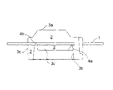
The figures la, 1 b, 1 c and id schematically illustrate an exemplary
embodiment of the invention, which is adapted to be used as a cavity-backed
slot-coupled patch antenna module for an AESA antenna. Indeed, the
5 invention enables to create a 3D-shaped integrated module with layer build-
ups that yields the bandwidth and scan-angle required by an AESA antenna.
A multilayer PCB insert 1 is laminated. The lamination material used is
selected in regard of its compatibility with a molding process. For example,
Rogers 4003 (TradeMark) is a lamination material that both resists high
temperature and pressure. Advantageously, Rogers 4003 is compatible with
most thermoplastic and thermoset molding materials and processes, which
means that it is adapted to establish a weld junction with most of these
molding materials when heated. For example, Rogers 4003 may be used in
association with a thermoset molding material like an epoxy resin. It may also
be used in association with a thermoplastic molding material like
polyetherimide (PEI) or liquid crystal polymer (LCP). In the present example,
PEI resin may be used. The insert 1 is pre-treated with an alkaline
conditioner, like an NaOH solution for example, and with sulfuric-peroxide
based chemistry, like AlfaPREP P0-7030 (TradeMark) for example, to create
an organo-metallic conversion coating. The multilayer PCB insert 1 is then
dried and inserted in a three-dimensional mold, like any conventional metal
insert. In the present example, PEI and LOP resin is heated, then injected in
the mold and pressured, resulting in a 3D moulded structure 2 encompassing
the multilayer PCB insert 1 by virtue of a weld junction. Afterwards,
metallization processes are applied to the outer surface of the 3D moulded
structure 2. A metallization pattern 3a forms a patch antenna. A metallization
pattern 3b is connected to an inner track pattern 4a of the multilayer PCB
insert 1. A metallization pattern 3c forms grounding layers and is connected
to a grounding layer 4b of the multiplayer PCB insert 1, the grounding layer
4b including metallized vias running through the insert 1.
The outer metallization patterns 3a, 3b and 3c may be applied by a
laser subtractive structuring technique. First, the outer surface of the 3D
moulded structure 2 may be chemically plated with copper in the range of 1
to 10 micrometers for example. Where needed, the thickness of this layer
may be increased up to several tens of micrometers by a galvanic copper
plating. After copper plating, a chemical tin layer of 0.1 to 1 micrometer may
CA 02671251 2009-07-03
6
be deposited and then patterned by a 3D laser structuring technique.
Afterwards, the tin layer may be used as a three-dimensional mask during
copper etching, after which the tin layer may be stripped. Another option
might be to metallize the outer surface of the 3D moulded structure 2 with a
suitable surface finish, for example nickel and gold. However, in any case,
the metallization process shall ensure that the outer metallization patterns
3b
and 3c are connected to the inner metallization patterns 4a and 4b. The
above mentioned process of preparing the multilayer PCB insert 1 before it is
inserted in the mold is intended to obtain a good adhesion between the insert
1 and the molding material in order to obtain a reliable interconnection.
After
removal of external features of the insert 1, as better illustrated by Figure
lc
and Figure id, a final 3D-MID radiator 5 is obtained.
The 3D-MID radiator 5 may be assembled onto a carrier so as to form
an antenna module.
It is to be understood that variations to the example described
above, such as would be apparent to the skilled addressee, may be made
without departing from the scope of the present invention.
The invention disclosed herein discloses a convenient, simple,
flexible and compact solution that may comply with requirements of other
high-end electronic applications than highly integrated radar applications.
For
example, the invention may comply with the requirements of the telecom
base stations. Considering its low cost in regard of its performance, the
present invention is a particularly cost-efficient solution.