Note: Descriptions are shown in the official language in which they were submitted.
CA 02671323 2009-06-01
WO 2008/066910 PCT/US2007/024651
Organic Photovoltaic Cells Utilizing Ultrathin Sensitizing Layer
Related Applications
[0001] This application is a continuation-in-part of U.S. Application No.
11/263,865 filed
November 2, 2005 (pending), the contents of which are incorporated herein by
reference.
United States Government Rights
[0002] This invention was made with U.S. Government support under Contract No.
339-4012
awarded by U.S. Department of Energy, National Renewable Energy Laboratory.
The
government has certain rights in this invention.
Joint Research Agreement
[0003] Portions of the claimed invention were made by, on behalf of, and/or in
connection
with one or more of the following parties to a joint university-corporation
research agreement
Princeton University, The University of Southern California, and Global
Photonic Energy
Corporation. The remainder of the claimed invention was made by, on behalf of,
and/or in
connection with one or more of the following parties to a joint university-
corporation research
agreement The University of Michigan, The University of Southern California,
and Global
Photonic Energy Corporation. The agreements were in effect on and before the
date the
respective portions of the claimed invention were made, and the claimed
invention was made as
a result of activities undertaken within the scope of the agreements.
Field of the Invention
[0004] The present invention generally relates to organic photosensitive
optoelectronic
devices. More specifically, it is directed to organic photosensitive
optoelectronic devices
including an ultra-thin low mobility active layer that is responsive to near
infrared.
CA 02671323 2009-06-01
WO 2008/066910 PCT/US2007/024651
Background
100051 Optoelectronic devices rely on the optical and electronic properties of
materials to
either produce or detect electromagnetic radiation electronically or to
generate electricity from
ambient electromagnetic radiation.
100061 Photosensitive optoelectronic devices convert electromagnetic radiation
into an
electrical signal or electricity. Solar cells, also called photovoltaic ("PV")
devices, are a type of
photosensitive optoelectronic device that is specifically used to generate
electrical power.
Photoconductor cells are a type of photosensitive optoelectronic device that
are used in
conjunction with signal detection circuitry which monitors the resistance of
the device to detect
changes due to absorbed light. Photodetectors, which may receive an applied
bias voltage, are a
type of photosensitive optoelectronic device that are used in conjunction with
current detecting
circuits which measures the current generated when the photodetector is
exposed to
electromagnetic radiation.
100071 These three classes of photosensitive optoelectronic devices may be
distinguished
according to whether a rectifying junction as defined below is present and
also according to
whether the device is operated with an external applied voltage, also known as
a bias or bias
voltage. A photoconductor cell does not have a rectifying junction and is
normally operated with
a bias. A PV device has at least one rectifying junction and is operated with
no bias. A
photodetector has at least one rectifying junction and is usually but not
always operated with a
bias.
[0008] As used herein, the term "rectifying" denotes, inter alia, that an
interface has an
asymmetric conduction characteristic, i.e., the interface supports electronic
charge transport
preferably in one direction. The term "semiconductor" denotes materials which
can conduct
electricity when charge carriers are induced by thermal or electromagnetic
excitation. The term
"photoconductive" generally relates to the process in which electromagnetic
radiant energy is
absorbed and thereby converted to excitation energy of electric charge
carriers so that the carriers
can conduct (i.e., transport) electric charge in a material. The term
"photoconductive material"
refers to semiconductor materials which are utilized for their property of
absorbing
electromagnetic radiation to generate electric charge carriers. As used
herein, "top" means
fiirthest away from the substrate, while "bottom" means closest to the
substrate. There may be
2
CA 02671323 2009-06-01
WO 2008/066910 PCT/US2007/024651
intervening layers, unless it is specified that the first layer is "in
physical contact with" the
second layer.
[0009] When electromagnetic radiation of an appropriate energy is incident
upon an organic
semiconductor material, a photon can be absorbed to produce an excited
molecular state. In
organic photoconductive materials, the excited molecular state is generally
believed to be an
"exciton," i.e., an electron-hole pair in a bound state which is transported
as a quasi-particle. An
exciton can have an appreciable life-time before geminate recombination
("quenching"), which
refers to the original electron and hole recombining with each other (as
opposed to
recombination with holes or electrons from other pairs). To produce a
photocurrent, the
electron-hole forming the exciton are typically separated at a rectifying
junction.
[0010] In the case of photosensitive devices, the rectifying junction is
referred to as a
photovoltaic heterojunction. Types of organic photovoltaic heterojunctions
include a donor-
acceptor heterojunction fornied at an interface of a donor material and an
acceptor material, and
a Schottky-barrier heterojunction formed at the interface of a photoconductive
material and a
metal.
[0011] FIG. I is an energy-level diagram illustrating an example donor-
acceptor
heterojunetion. In the context of organic materials, the terms "donor" and
"acceptor" refer to the
relative positions of the Highest Occupied Molecular Orbital ("HOMO") and
Lowest
Unoccupied Molecular Orbital ("LUMO") energy levels of two contacting but
different organic
materials. If the LUMO energy level of one material in contact with another is
lower, then that
material is an acceptor. Otherwise it is a donor. It is energetically
favorable, in the absence of
an external bias, for electrons at a donor-acceptor junction to move into the
acceptor material.
[0012] As used herein, a first HOMO or LUMO energy level is "greater than" or
"higher than"
a second HOMO or LUMO energy level if the first energy level is closer to the
vacuum energy
level 10. A higher HOMO energy level corresponds to an ionization potential
("IP") having a
smaller absolute energy relative to a vacuum level. Similarly, a higher LUMO
energy level
corresponds to an electron affinity ("EA") having a smaller absolute energy
relative to vacuum
level. On a conventional energy level diagram, with the vacuum level at the
top, the LUMO
energy level of a material is higher than the HOMO energy level of the same
material.
CA 02671323 2009-06-01
WO 2008/066910 PCT/US2007/024651
[0013] After absorption of a photon 6 in the donor 152 or the acceptor 154
creates an exciton
8, the exciton 8 dissociates at the rectifying interface. The donor 152
transports the hole (open
circle) and the acceptor 154 transports the electron (dark circle).
[0014] A significant property in organic semiconductors is carrier mobility.
Mobility
measures the ease with which a charge carrier can move through a conducting
material in
response to an electric field. In the context of organic photosensitive
devices, a material that
conducts preferentially by electrons due to a high electron mobility may be
referred to. as an
electron transport material. A material that conducts preferentially by holes
due to a high hole
mobility may be referred to as a hole transport material. A layer that
conducts preferentially by
electrons, due to mobility and / or position in the device, may be. referred
to as an electron
transport layer ("ETL"). A layer that conducts preferentially by holes, due to
mobility and / or
position in the device, may be referred to as a hole transport layer ("HTL").
Preferably; but not
necessarily, an acceptor material is an electron transport material and a
donor material is a hole
transport material. [0015] How to pair two organic photoconductive materials
to serve as a donor and an acceptor
in a photovoltaic heterojunction based upon carrier niobilities and relative
HOMO and LUMO
levels is well known in the art, and is not addressed here.
[0016] One common feature of bulk semiconductors, as well as insulators, is a
"band gap."
The band.gap is the energy difference between the highest energy level filled
with electrons and
the lowest energy level that is empty. In an inorganic semiconductor or
inorganic insulator, this
energy difference is the difference between the valence band edge (top of the
valence band) and
the conduction band edge (bottom of the conduction band). In an organic
semiconductor or
organic insulator, this energy difference is the difference between the HOMO
and the LUMO.
The band gap of a pure material is devoid of energy states where electrons and
holes can exist.
The only available carriers for conduction are the electrons and holes which
have enough energy
to be excited across the band gap. In general, semiconductors have a
relatively small band gap in
comparison to insulators.
100171 In terms of an energy band model for organic semiconductors, only
electrons on the
LUMO side of the band gap are charge carriers, and only holes on the HOMO side
of the band
gap are charge carriers.
4
CA 02671323 2009-06-01
WO 2008/066910 PCT/US2007/024651
[0018] As used herein, the term "organic" includes polymeric materials as well
as small
molecule organic materials that may be used to fabricate organic opto-
electronic devices. "Small
molecule" refers to any organic material that is not a polymer, and "small
molecules" may
actually be quite large. Small molecules may include repeat units in some
circumstances. For
example, using a long chain alkyl group as a substituent does not remove a
molecule from the
"small molecule" class. Small molecules may also be incorporated into
polymers, for example.
as a pendent group on a polymer backbone or as a part of the backbone. Small
molecules may
also serve as the core moiety of a dendrimer, which consists of a series of
chemical shells built
on the core moiety. The core moiety of a dendrimer may be a fluorescent or
phosphorescent
small molecule emitter. A dendrimer may be a "small molecule." In general, a
small molecule
has a defined chemical formula with a molecular weight that is the same from
molecule to
molecule, .whereas a polymer has a defined chemical formula with a molecular
weight that may
vary from molecule to molecule. As used herein, "organic" includes metal
complexes of
hydrocarbyl and heteroatom-substituted hydrocarbyl ligands.
[0019] For additional background explanation and description of the state of
the art for organic
photosensitive devices, including their general c,-)nstruction,
characteristics, materials, and
features, U.S. Patent No. 6,657,378 to Forrest et al., U.S. Patent No.
6,580,027 to Forrest et crl.,
and U.S. Patent No. 6,352,777 to Bulovic et al. are incorporated herein by
reference.
Summary of the Invention
[0020] A photosensitive device includes a plurality of organic photoconductive
materials
disposed in a stack between a first electrode and a second electrode,
including a first continuous
layer of donor host material, a second continuous layer of acceptor host
material, and at least one
other organic photoconductive inaterial disposed as a plurality of
discontinuous islands between
the first continuous layer and the second continuous layer. Each of these
other photoconductive
materials has an absorption spectra different from the donor host material and
the acceptor host
material.
[0021] Preferably, each of the discontinuous islands consists essentially of a
crystallite of the
respective organic photoconductive material. The crystallites are preferably
nanocrystals, each
of the discontinuous islands having no dimension greater than 100 nm. More
preferably, a
distance from any point within each of the islands to a boundary of the island
is not more than
CA 02671323 2009-06-01
WO 2008/066910 PCT/US2007/024651
one exciton'diffusion length of the respective organic photoconductive
material for a majority of
the islands of each organic photoconductive material.
[0022] The first continuous layer may be in direct contact with the second
continuous layer in-
between the islands of the other organic photoconductive materials.
[0023] At least one of the other organic photoconductive materials is
preferably a small
molecule. Likewise, the donor host material and the acceptor host material are
preferably small
molecules.
[0024] As an example of an organic photoconductive material arranged as a
sensitizer, a band
gap of at least one of the other organic photoconductive materials is less in
magnitude (i.e., the
absolute value of the difference between HOMO and LUMO) than a band gap of the
donor host
material and less than a band gap of the acceptor host material. As another
example of an
organic photoconductive material arranged as a sensitizer, a band gap of at
least one of the other
organic photoconductive materials is greater in magnitude than a band gap of
the donor host
material and greater than a band gap of the acceptor host material. As yet
another example of an
organic photoconductive material arranged as a sensitizer, a band gap of at
least one of the other
organic photoconductive nlaterials is in between (in magnitude) a band gap of
the donor host
material and a band gap of the acceptor host material. If plural sensitizers
are included,
sensitizers having band gaps reflecting each of these examples can be included
in a same
photoactive region.
[0025] As an example, at least one organic photoconductive material of the
other organic
photoconductive materials may have a hole mobility of less than 1 x 10"9
cm2/Vs and an
absorption coefficient of at least 5 x 104 cm"1 across a wavelength band from
600 nm to 900 nm.
[0026] Preferred example sensitizer materials include tin (II) phthalocyanine
(SnPc) and lead
phthalocyanine (PbPc). With such sensitizers, a preferred acceptor host
material is C60.
[0027] At least one sensitizer preferably has an absorption coefficient of at
least 5 x 10⁴ em-1
across a wavelength band from 600 nm to 900 nn1.
[0028] The device may include a reflective surface. At least a portion of the
islands of a
sensitizer having an absorption coefficient of at least 5 x 104 cm-1 across a
wavelength band from
600 nm to 900 nm are disposed at an optical path length of X1=d +X1/4 from the
reflective
surface of the device, where Xi is a wavelength in the wavelength band from
600 nm to 900 nm,
6
CA 02671323 2009-06-01
WO 2008/066910 PCT/US2007/024651
d is an integer > 0, and the reflective surface is reflective to at least 50%
of incident light at Xi.
The reflective surface may be provided, for example, by one of the first
electrode, the second
electrode, and a reflector.
[0029] The device may be arranged in a tandem structure including plural
photoactive regions.
For example, the plurality of organic photoconductive materials may be part of
a first cell in a
stack of photoactive cells disposed between the first electrode and the second
electrode. The
tandem device further includes at least a second cell of the stack of
photoactive cells, the second
cell comprising at least one donor-acceptor heterojunction. Preferably, the
first cell and the
second cell have different absorption characteristics, an average absorption
of the first cell is
greater than the average absorption of the second cell over a range of
wavelengths X1 .5%, and
an average absorption of the second cell is greater than the average
absorption of the first cell
over a range of wavelengths X2 5%, where ~> >k2 + 10%.
[0030] .The plurality of discontinuous islands may include islands of multiple
different
sensitizers. Preferably, no more than 11 different sensitizers are included in
a single photoactive
region. For example, in one photoactive region, there may be islands of a
first sensitizer of the
other photoconductive materials and islands of a second sensitizer of the
other photoconductive
materials, with the first sensitizer having an absorption spectra different
from the second
sensitizer. The preferred limit of no more than 11 sensitizers applies to a
single pllotoactive
region, and in a tandem arrangement, each photoactive region preferably
includes at least some
different sensitizers. For example, two photoactive regions might include two
completely
separate or partially overlapping sets (in terms of materials selected) of
sensitizers, each set
including no more than 11 sensitizers in number.
[0031] If multiple sensitizers are included in a photoactive region, a
distance from any point
withiil each island of a first sensitizer to a boundary of the island is
preferably not more than one
excitoii diffiision length of the sensitizer material (i.e., the respective
organic photoconductive
material) for a majority of the islands of the first sensitizer, and a
distance from any point within
each island of the second sensitizer to a boundary of the island is not more
than one exciton
diffusion length of the second sensitizer for a majority of the islands of the
second sensitizer.
[0032] A method of fabricating a photosensitive optoelectronic device includes
depositing a
first organic pllotoconductive material over a first electrode to form a first
continuous layer,
depositing a second organic photoconductive material over the first continuous
layer to form a
7
CA 02671323 2009-06-01
WO 2008/066910 PCT/US2007/024651
first discontinuous layer comprising a plurality of islands, depositing a
third organic
photoconductive material over the first discontinuous layer to form a second
continuous layer,
and depositing a second electrode over the second continuous layer. One of the
first organic
photoconductive material and the second organic photoconductive material
consists essentially
of a donor host material, and an other of the first organic photoconductive
material and the
second organic photoconductive material consists essentially of an acceptor
host material. The
second organic photoconductive material is a sensitizer having an absorption
spectra different
from the donor host material and the acceptor host material.
[0033] Preferably, each island consists essentially of a crystallite of the
second organic
photoconductive material. The crystallites are preferably nanocrystals, such
that during the
deposition of the second organic photoconductive material, each area of
material growth
contributes no more than 100 nm of growth in any dimension. More preferably, a
distance from
any point within each of the islands to a boundary of the island is not more
than one exciton
diffusion length of the second organic photoconductive material for a majority
of the islands of
the second organic photoconductive inaterial.
[0034] A thickness of the first discontinuous layer is preferably not greater
than 200 A. More
preferably, a thickness of the first discontinuous layer is not greater than
100 A.
[0035] Other discontinuous layers may also be deposited. For example, the
method may
further include depositing a fourth organic photoconductive material, after
depositing the first
discontinuous layer but before depositing the second continuous layer, to form
a second
discontinuous layer comprising a plurality of islaiids, each island consisting
essentially of a
crystallite of the fourth organic photoconductive material. The fourth organic
photoconductive
material is a sensitizer having an absorption spectra different from the donor
host material, the
acceptor host material, and the second organic photoconductive material.
During the depositing
of the fourth organic photoconductive material, each area of material growth
preferably
contributes no more than 100 nnl of growth in any dimension.
[0036] Preferably at least one (or all) of the sensitizers, as well as the
donor and the acceptor,
are small molecule materials. For example, the first, second, third, and
fourth organic
photoconductive materials may be small molecule materials.
[0037] The method may further include sequentially depositing additional
organic
photoconductive materials, after depositing the fourth organic photoconductive
material but
8
CA 02671323 2009-06-01
WO 2008/066910 PCT/US2007/024651
before depositing the second continuous layer, to form additional
discontinuous layers
comprising islands. Preferably, each island consists essentially of a
crystallite of the respective
organic photoconductive material, and during the depositing of each additional
organic
photoconductive material, each area of material growth contributes no more
than 100 nm of
growth in any dimension. Each additional organic photoconductive material is a
sensitizer
having an absorption spectra different from the donor host material, the
acceptor host material,
and the other sensitizers (including the second and fourth organic
photoconductive materials in
the example above). Preferably, not more than 11 different sensitizers are
deposited between the
first continuous layer and the second continuous layer (i.e., not more than 11
different sensitizers
are deposited in a single photoactive region).
[0038] As noted in the discussion of the finished device above, an example of
an organic
photoconductive material arranged as a sensitizer is if the second organic
photoconductive
material has a band gap that is less than a band gap of the donor host
material and less than a
band gap of the acceptor host material. As another example, the second organic
photoconductive
material may have a band gap that is greater than a band gap of the donor host
inaterial and
greater than a band gap of the acceptor host material. As yet another
exanlple, the second
organic photoconductive material may have a band gap in between a band gap of
the donor host
material and a batid gap of the acceptor host material. If plural sensitizers
are deposited,
sensitizers having band gaps reflecting each of these examples can be
deposited into what will be
come a same pliotoactive region.
Brief Description of the Drawings
100391 FIG. I is an energy level diagram illustrating a donor-acceptor
heterojunction.
[0040] FIG. 2 illustrates an organic photosensitive device including a donor-
acceptor
heterojunction.
[0041] FIG. 3 illustrates a donor-acceptor bilayer forming a planar
heterojunction.
[0042] FIG. 4 illustrates a hybrid heterojunction including a mixed
heterojunction between a
donor layer and an acceptor layer.
[0043] FIG. 5 illustrates a bulk heterojunction.
[00441 FIG. 6 illustrates an organic photosensitive device including a
Schottky-barrier
heterojunction.
9
CA 02671323 2009-06-01
WO 2008/066910 PCT/US2007/024651
[0045] FIG. 7 illustrates tandem photosensitive cells in series.
[0046] FIG. 8 illustrates tandem photosensitive cells in parallel.
[0047] FIG. 9 illustrates a planar heterojunction modified to include an
additional thin
photoactive layer.
[0048] FIG. 10A illustrates a cross-section of an example of the thin
photoactive layer.
[0049] FIG. I OB illustrates a cross-section of another example of the thin
protective layer.
[0050] FIG. 11 illustrates an energy level diagram including the thin
photoactive layer as a
donor.
100511 FIG. 12 illustrates. an energy level diagram including the thin
photoactive layer as an
acceptor.
[0052] FIG. 13 illustrates a hybrid heterojunction including the thin
photoactive layer as a
donor.
[0053] FIG. 14 illustrates a hybrid heterojunction including the thin
photoactive layer as an
acceptor.
100541 FIG. 15 illustrates u planar heterojunction including a plurality of
thin photoactive
layers.
100551 FIG. 16 illustrates an energy level diagram including the plurality of
thin photoactive
layers for the planar heterojunction in FIG. 15.
[0056] FIG. 17 illustrates an energy level diagram including a plurality of
thin photoactive
layers of sensitizer materials between a donor and an acceptor arranged to
form an energy
cascade.
[0057] FIG. 18 demonstrates the relative HOMO and LUMO levels and energy gaps
for a
variety of organic photoconductive materials as non-exclusive examples of
materials that can be
used within the photoactive region of a hybrid planar-nanocrystalline bulk
heterojunction as
donors, acceptors, and sensitizers.
[0058] FIG. 19 illustrates the positioning of the various layers to maximize
absorption by the
thin photoactive layer.
[0059] FIG. 20 illustrates an energy level diagram for an example arrangement
of four
photoconductive materials.
CA 02671323 2009-06-01
WO 2008/066910 PCT/US2007/024651
[0060] FIG. 21 illustrates the normalized absorption spectra for the materials
in FIG. 20.
[0061] FIG. 22 is an AM 1.5G radiation spectrum (for reference).
[0062] FIGS. 23A-23G illustrate steps for forming an example device including
nanocrystal
sensitizer layers.
[0063] FIG. 24 illustrates a circuit utilizing the device formed by the method
in FIGS. 23A-
23G.
[0064] The device structure figures are not necessarily drawn to scale.
Detailed Description
[0065] An organic photosensitive device comprises at least one photoactive
region in which
light is absorbed to form an exciton, which may subsequently dissociate into
an electron and a
hole. FIG. 2 shows an example of an organic photosensitive optoelectronic
device 100 in which
the photoactive region 150 comprises a donor-acceptor heterojunction. The
"photoactive region"
is a portion of a photosensitive device that absorbs electromagnetic radiation
to generate excitons
that may dissociate in order to generate an electrical current. Device 100
comprises an anode
120, an anode smoothing layer 122, a donor 152, an acceptor 154, an exciton
blocking layer
("EBL") 156, and a cathode 170, over a substrate 110.
[0066] Exanlples of EBL 156 are described in U.S. Patent No. 6,451,415 to
Forrest et al.,
whicli is incorporated herein by reference for its disclosure related to EBLs.
Additional
background explanation of EBLs may also be found in Peumans et al., "Efficient
photon
harvesting at high optical intensities in ultrathin organic double-
lieterostructure photovoltaic
diodes," Applied Physics Letters 76, 2650-52 (2000). EBLs (among other things)
reduce
quenching by preventing excitons from migrating out of the donor and/or
acceptor materials.
[0067] The terms "electrode" and "contact" are used interchangeably herein to
refer to a layer
that provides a medium for delivering photo-generated current to an external
circuit or providing
a bias current or voltage to the device. As illustrated in FIG. 2, anode 120
and cathode 170 are
examples. Electrodes may be composed of metals or "metal substitutes." Herein
the term
"metal" is used to embrace both materials composed of an elementally pure
metal, and also metal
alloys which are materials composed of two or more elementally pure metals.
The term "metal
substitute" refers to a material that is not a metal within the normal
definition, but which has the
nletal-like properties such as conductivity, such as doped wide-bandgap
semiconductors,
11
CA 02671323 2009-06-01
WO 2008/066910 PCT/US2007/024651
degenerate semiconductors, conducting oxides, and conductive polymers.
Electrodes may
comprise a single layer or multiple layers (a "compound" electrode), may be
transparent, semi-
transparent, or opaque. Examples of electrodes and electrode materials include
those disclosed
in U.S. Patent No. 6,352,777 to Bulovic et al., and U.S. Patent No. 6,420,031,
to Parthasarathy,
et al., each incorporated herein by reference for disclosure of these
respective features. As used
herein, a layer is said to be "transparent" if it transmits at least 50% of
the ambient
electromagnetic radiation in a relevant wavelength.
[0068] The substrate 110 may be any suitable substrate that provides desired
structural
properties. The substrate may be flexible or rigid, planar or non-planar. The
substrate may be
transparent, translucent or opaque. Rigid plastics and glass are examples of
preferred rigid
substrate materials. Flexible plastics and metal foils are examples of
preferred flexible substrate
materials.
[0069] An anode-smoothing layer 122 may be situated between the anode layer
120 and the
donor layer 152. Anode-smoothing layers are described in U.S. Patent 6,657,378
to Forrest et
al., incorporated here:n by reference for its disclosure related to this
feature.
[0070] In FIG. 2, the photoactive region 150 comprises the donor material 152
and the
acceptor material 154. Organic materials for use in the photoactive region may
include
organometallic compounds, including cyclometallated organometallic compounds.
The ternl
"organometallic" as used llerein is as generally understood by one of ordinary
skill in the art and
as given, for example, in Chapter 13 of "Inorganic Chemistry" (2nd Edition) by
Gary L. Miessler
and Donald A. Tarr, Prentice Hall (1999).
100711 Organic layers may be fabricated using vacuum deposition, spin coating,
organic
vapor-phase deposition, organic vapor jet deposition, inkjet printing and
other methods known in
the art.
[0072] Examples of various types of donor-acceptor heterojunctions are shown
in FIGS. 3-5.
FIG. 3 illustrates a donor-acceptor bilayer forming a planar heterojunctioil.
FIG. 4 illustrates a
hybrid heterojunction including a mixed heterojunction 153 comprising a
mixture of donor and
acceptor materials arranged between the donor material 152 and the acceptor
material 154. FIG.
illustrates an idealized "bulk" heterojunction. A bulk heterojunction 253, in
the ideal
photocurrent case, has a single cotltinuous interface between the donor
material 252 and the
acceptor material 254, although multiple interfaces typically exist in actual
devices. Mixed and
12
CA 02671323 2009-06-01
WO 2008/066910 PCT/US2007/024651
bulk heterojunctions can have multiple donor-acceptor interfaces as a result
of having plural
domains of material. Domains that are surrounded by the opposite-type material
(e.g., a domain
of donor material surrounded by acceptor material) may be electrically
isolated, such that these
domains do not contribute to photocurrent. Other domains may be connected by
percolation
pathways (continuous photocurrent pathways), such that these other domains may
contribute to
photocurrent. The distinction between a mixed and a bulk heterojunction lies
in degrees of phase
separation between donor and acceptor materials. In a mixed heterojunction,
there is very little
or no phase separation (the domains are very small, e.g., less than a few
nanometers), whereas in
a bulk heterojunction, there is significant phase separation (e.g., forming
domains with sizes of a
few nanometers to 100 nm).
[0073] Small-molecule mixed heterojunctions may be formed, for example, by co-
deposition
of the donor and acceptor materials using vacuum deposition or vapor
deposition. Small-
molecule bulk heterojunctions may be formed, for example, by controlled
growth, co-deposition
with post-deposition annealing, or solution processing. Polymer mixed or bulk
heterojunctions
may be formed, for example, by solution processing of polyiner blends of donor
and acceptor
materials.
[00741 If a photoactive region includes a mixed layer (153) or bulk layers
(252, 254) and one
or both of the donor (152) and acceptor layers (154), the photoactive region
is said to include a
"hybrid" heterojunction. The arrangement of layers in FIG. 4 is an example.
For additional
explanation of hybrid heterojunctions, U.S. Published Patent Application 2005-
02241 13 Al
entitled "'High efficiency organic photovoltaic cells employing hybridized
mixed-planar
heterojunctions" by Jiangeng Xue et al., published October 13, 2005, is hereby
incorporated by
reference.
[0075] In general, planar heterojunctions have good carrier conduction, but
poor exciton
dissociation; a mixed layer has poor carrier conduction and good exciton
dissociation, and a bulk
heterojunction has good carrier conduction and good exciton dissociation, but
may experience
charge build-up at the end of the material "cul-de-sacs," lowering efficiency.
Unless otherwise
stated, planar, mixed, bulk, and hybrid heterojunctions may be used
interchangeably as donor-
acceptor heterojunctions throughout the embodiments disclosed herein.
[0076] FIG. 6 shows an example of a organic photosensitive optoelectronic
device 300 in
which the photoactive region 350 is part of a Schottky-barrier heterojunction.
Device 300
13
CA 02671323 2009-06-01
WO 2008/066910 PCT/US2007/024651
comprises a transparent contact 320, a photoactive region 350 comprising an
organic
photoconductive material 358, and a Schottky contact 370. The Schottky contact
370 is typically
formed as a metal layer. If the photoconductive layer 358 is an ETL, a high
work function metal
such as gold may be used, whereas if the photoconductive layer is an HTL, a
low work function
metal such as aluminum, magnesium, or indium may be used. In a Schottky-
barrier cell, a built-
in electric field associated with the Schottky barrier pulls the electron and
hole in an exciton
apart. Generally, this field-assisted exciton dissociation is not as efficient
as the dissociation at a
donor-acceptor interface.
100771 The devices as illustrated may be connected to an element 190. If the
device is a
photovoltaic device, element 190 is a resistive load which consumes or stores
power. If the
device is a photodetector, element 190 is a current detecting circuit which
measures the current
generated when the photodetector is exposed to light, and which may apply a
bias to the device
(as described for example in Published U.S. Patent Application Publication
2005-0110007 Al,
published May 26, 2005 to Forrest et al.). If the rectifying junction is
eliminated from the device
(e.g., using asingle photoconductive material as the photoactive region), the
resulting structures
may be used :.ts a photoconductor cell, in which case the element 190 is a
signal detection circuit
to monitor changes in resistance across the device due to the absorption of
light. Unless
otherwise stated, each of these arrangements and modifications may be used for
the devices in
each of the drawings and embodiments disclosed herein.
100781 An organic photosensitive optoelectronic device may also comprise
transparent charge
transfer layers, electrodes, or charge recombination zones. A charge transfer
layer may be
organic or inorganic, and may or may not be photoconductively active. A charge
transfer layer is
similar to an electrode, but does not have an electrical connection external
to the device and
delivers charge carriers from one subsection of an optoelectronic device to
the adjacent
subsection. A charge recombination zone is similar to a charge transfer layer,
but allows for the
reconlbination of electrons and holes between adjacent subsections of an
optoelectronic device.
A charge recombination zone may include semi-transparent metal or metal
substitute
recombination centers comprising nanoclusters, nanoparticles, and/or nanorods,
as described for
example in U.S. Patent No. 6,657,378 to Forrest et al.; U.S. Patent
Application 10/915,410
entitled "Organic Photosensitive Devices" by Rand et al., filed August 11,
2004 (now Published
U.S. Patent Application Publication 2006-0032529 Al); and U.S. Patent
Application 10/979,145
14
CA 02671323 2009-06-01
WO 2008/066910 PCT/US2007/024651
entitled "Stacked Organic Photosensitive Devices" by Forrest et al., filed
November 3, 2004
(now Published U.S. Patent Application Publication 2006-0027802 Al); each
incorporated
herein by reference for its disclosure of recombination zone materials and
structures. A charge
recombination zone may or may not include a transparent matrix layer in which
the
recombination centers are embedded. A charge transfer layer, electrode, or
charge
recombination zone may serve as a cathode and/or an anode of subsections of
the optoelectronic
device. An electrode or charge transfer layer may serve as a Schottky contact.
[0079] FIGS. 7 and 8 illustrate examples of tandem devices including such
transparent charge
transfer layers, electrodes, and charge recombination zones. In device 400 in
FIG. 7, photoactive
regions 150 and 150' are stacked electrically in series with an intervening
conductive region 460.
As illustrated without external electrical connections, intervening conductive
region 460 may be
a charge recombination zone or may be a charge transfer layer. As a
recombination zone, region
460 comprises recombination centers 461 with or without a transparent matrix
layer. If there is
no matrix layer, the arrangement of material forming the zone may not be
continuous across the
region 460. Device 500 in FIG. 8 illustrates photoactive regions 150 and 150'
stacked
electrical!y in parallel, with the top cell being in an inverted configuration
(i.e., cathode-down).
In each of FIGS. 7 and 8, the photoactive regions 150 and 150' and blocking
layers 156 and 156'
may be fornled out of the same respective materials, or different materials,
depending upon the
application. Likewise, photoactive regions 150 and 150' may be a same type
(i.e., planar, mixed,
bulk, hybrid) of heterojunction, or may be of different types.
[0080] In eacll of the devices described above, layers may be omitted, such as
the exciton
blocking layers. Other layers may be added, such as reflective layers or
additional photoactive
regions. The order of layers may be altered or inverted. A concentrator or
trapping
configuration may be employed to increase efficiency, as disclosed, for
example in U.S. Patent
No. 6,333,458 to Forrest et al. and U.S. Patent No. 6,440,769 to Peumans et
al., which are
incorporated herein by reference. Coatings may be used to focus optical energy
into desired
regions of a device, as disclosed, for example in US Patent Application No.
10/857,747 entitled
"Aperiodic dielectric multilayer stack" by Peumans et al., filed June 1, 2004
(now Published
U.S. Patent Application Publication US 2005-0266218 Al), which is incorporated
herein by
reference. In the tandem devices, transparent insulative layers may be formed
between cells,
with the electrical connection between the cells being provided via
electrodes. Also in the
CA 02671323 2009-06-01
WO 2008/066910 PCT/US2007/024651
tandem devices, one or more of the photoactive regions may be a Schottky-
barrier heterojunction
instead of a donor-acceptor heterojunction. Arrangements other than those
specifically described
may be used.
[00811 Photovoltaic devices produce a photo-generated current when they are
connected
across a load and are irradiated by light. When irradiated under infinite
load, a photovoltaic
device generates its maximum possible voltage, V open-circuit, or Voc. When
irradiated with its
electrical contacts shorted, a photovoltaic device generates its maximum
possible current, I short-
circuit, or Isc. When actually used to generate power, a photovoltaic device
is connected to a
finite resistive load and the power output is given by the product of the
current and voltage, I XV.
The maximum total power generated by a photovoltaic device is inherently
incapable of
exceeding the product, Isc x Voc. When the load value is optimized for maximum
power
extraction, the current and voltage have the values, Imax and Vmax,
respectively.
[0082] A figure of merit for photovoltaic devices is the fill factor, ff,
defined as:
ff-{Iniax Umax}/{ISCVOC}
where ff is alxvays less than 1, as Isc and Voc are never obtained
simultaneously in actual use.
Nonetheless; as ff approaches 1, the device has less series or internal
resistance and thus delivers
a greater percentage of the product of Isc and Voc to the load under optimal
conditions. Where
Pinc is the power incident on a device, the power efficiency of the device, p,
may be calculated
by:
P -ff* (Isc * Voc) / Pinc
[0083] Organic photovoltaic cells have many potential advantages when compared
to
traditional silicon-based devices. Organic photovoltaic cells are light
weight, economical in
materials use, and can be deposited on low cost substrates, such as flexible
plastic foils.
However, soine organic photovoltaic devices typically have relatively low
external quantum
efficiency, being on the order of 1% or less. This is, in part, thought to be
due to the second
order nature of the intrinsic photoconductive process. That is, carrier
generation requires exciton
generation, diffusion and ionization or collection. There is an efficiency
associated with each of
these processes. Subscripts may be used as follows: P for power efficiency,
EQE for external
16
CA 02671323 2009-06-01
WO 2008/066910 PCT/US2007/024651
quantum efficiency, A for photon absorption, ED for exciton diffusion, CC for
charge collection,
and INT for internal quantum efficiency. Using this notation:
_- * *
r1P ~ IJEQE IIA IIED TICC
- *
rIEQE IJA TI[NT
[0084] Photodetectors and photovoltaic (PV) cells using small molecular weight
organic thin
films deposited on plastic substrates have the potential advantages of being
low-cost and
lightweight. See S. R. Forrest, "The path to ubiquitous and low-cost organic
electronic.
appliances on plastic," Nature 428, 911-918 (2004). Recently, the power
conversion efficiency
of molecular organic PV cells has steadily improved due to the use of new
materials and. device
architectures. See S. R. Forrest, "The Limits to Organic Photovoltaic Cell
Efficiency," =MRS
Bulletin 30, 28-32 (2005); and J. Xue et al., "Asymmetric tandem organic
photovoltaic=cells with
hybrid planar-mixed molecular heterojunctions," Applied Physics Letters 85,
5757-5759 (2004).
[00851 One problem with organic PV energy conversion, however, is the limited
overlap
between the active layer absorption with the solar spectrum. Indeed, over 60%
of the total solar
photon flux is at wavelengths k > 600 nn1 with approxiniately 50% in the red
and near infrared
(NIR) spectrum at 600 <), < 1000 nm. Therefore, new materials need to be
developed that can
absorb NIR radiation, and efficiently convert absorbed photons into current.
[0086] Recently, a polymer-based solar cell sensitive to NIR radiation up to
1000 nm
achieved a power conversion efficiency of 0.3% under I sun illumination. See
X. J. Wang et al.,
Applied Physics Letters 85, 5081 (2004). However, previous efforts with small
molecule
materials have failed to extend device responsivity into NIR.
[0087] Research into developing a small molecule photosensitive device has
yielded a new
architecture which, in addition to achieving NIR responsivity, may be used to
tune and/or
broaden the sensitivity of any donor-acceptor heterojunction. By incorporating
a thin sensitizing
layer between donor and acceptor, this new architecture enables the
construction of
photosensitive devices which retain their overall device thickness, but which
can produce
photocurrent in a part of the spectrum otherwise inaccessible using other
materials.
[0088] In addition, a larger array of different materials are available for
use as the thin
sensitizing layer than would otherwise be viable as either a conventional
donor or acceptor layer.
17
CA 02671323 2009-06-01
WO 2008/066910 PCT/US2007/024651
For example, a material having low charge carrier mobility can be employed
without a loss of
device performance. By pairing the thin sensitizing layer with an
energetically favorable donor
or acceptor layer, the thin sensitizing layer contributes to photocurrent,
without impeding carrier
transport between the donor and acceptor.
[0089] FIG. 9 illustrates a donor-acceptor heterojunction, as used in the
devices (e.g., 100,
400, 500) discussed above, modified to incorporate the new thin sensitizing
layer 980 within a
photoactive region 950. The thin sensitizing layer 980 comprises a host
material that is different
from either that of the donor 152 or the acceptor 154. A "host material" of an
organic
photoactive layer, as defined herein, is a photoactive organic molecule making
up more than
50% molar of the respective layer. The thin sensitizing layer 980 may be
configured as a donor
or as an acceptor. In any case, a distance from any point within the host
material of the
sensitizing layer 980 to a boundary of that layer is preferably not more than
one exciton diffusion
length over a majority (> 50%) of the area of the thin sensitizing layer 980.
An exciton diffusion
length is the travel distance over which 1/e excitons decay/recombine. The
distance is over a
"majority" of the area since the layer 980 may include edge effects and snlall
variations in iocal
thickness (e.g., bumps and beads). Preferably, edge effects and the like are
avoided, and the
distaiice from any point within the host material of the thin sensitizing
layer 980 to a boundary of
that layer is not nlore than one exciton diffusion length over an entirety of
the area of the thin
sensitizing layer 980. Preferably, even if twice this distance across the
sensitizing layer 980 is
more than 200 A, the layer thickness is no greater than 200 A. More
preferably, the layer
thickness is no greater than 100A.
[0090] Due to efficiency concerns, a balance may be struck between the
thinness and the
photocurrent contribution of the sensitizing layer 980. Favoring a thin layer
is the desire to
minimize resistivity across the photoactive layer for carriers transiting
between donor layer 152
and acceptor layer 154, and maximizing the ability of excitons formed in the
sensitizing layer
980 to reach a rectifying interface. Favoring a thick layer is the volume in
which photons can be
absorbed in the absorption wavelength band of the sensitizing layer 980. While
two exciton
diffusion lengths is an idealized thickness upper limit, it is expected that
for most material
combinations and light-source spectra, a thinner sensitizing layer 980 is
desirable.
[0091) While the thin sensitizing layer 980 may be solid, it may instead be
porous, as
illustrated in FIG. 10A. If porous, the sensitizing layer 980 includes a
plurality of pathways
18
CA 02671323 2009-06-01
WO 2008/066910 PCT/US2007/024651
1001 (i.e., openings) through a unitary layer. The adjacent layers (e.g., the
donor 152 and the
acceptor 154) directly contact each other through the pathways 1001, providing
charge carriers a
direct path between layers. The pathways 1001 can manifest during the
deposition process due
to, for example, using such a thin layer 980 that there is a natural
irregularity to coverage (e.g.,
growth until material nucleation sites connect, but before all gaps are
filled), or by having
surface irregularity in the underlying layer (e.g., donor 152) that results in
irregular coverage.
100921 FIG. l OB is another example of thin layer 980. In this example, the
layer comprises a
plurality of discontinuous islands of material. The islands 1002 can manifest
during the
deposition process due to, for example, stopping growth shortly after
nucleation.
100931 A solid layer, a discontinuous layer of islands, or a porous unitary
layer may be
selected during fabrication simply by controlling how long growth is allowed
to continue after
material nucleation: While all three styles of layer 980 are operable, the
discontinuous layer of
islands is preferred. More preferably, the islands each comprise a crystallite
of the respective
photoconductive material, each crystallite having no dimension greater than
100 nm (i.e.,
nanocrystals).
[0094[ Among the advantages of nanocrystals is improved carrier mobility and
lower series
resistance in comparison to amorphous-phase islands. Moreover, a quasi-random
arrangement of
nanocrystals, including plural discontinuous layers of different
photoconductive materials,
enhances performance since the quasi-random distribution of crystals increases
the occurrence of
conductive pathways for collection of photo-generated charge carriers and
further enhances the
absorption of light due to the ability to form thicker devices. Preferably,
the continuous donor
layer 152 and the continuous acceptor layer 154 are also polycrystalline or
monocrystalline.
[0095] Preferably, the thin sensitizing layer 980 is a small molecule
material. Likewise, it is
preferred at the donor layer 152 and acceptor layer 154 also be small molecule
materials.
However, while small molecules are preferred, polymers can also be used for
one or more of the
sensitizers, donor, and acceptor, depending on the deposition method as
described further below.
[0096] To absorb NIR, the sensitizing material should preferably have an
absorption
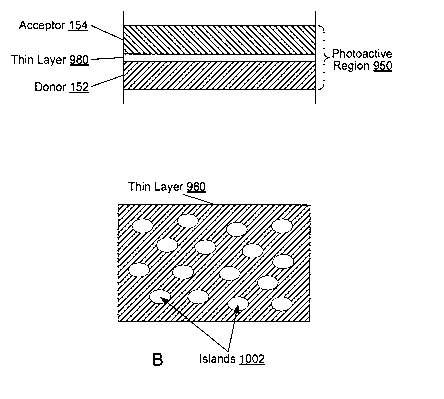
coefficient of at least 5 x 10⁴ cin-1 across a wavelength band from 600 nm to
900 nm. To
maximize coverage of the absorption spectra, the three photoactive layers
(152, 980, 154) should
preferably each have a different absorption spectra.
19
CA 02671323 2009-06-01
WO 2008/066910 PCT/US2007/024651
[0097] Referring to FIG. 11, the thin sensitizing layer 980 may serve as a
donor, having a
different host material than donor layer 152. Preferably for such an
arrangement, the HOMO of
the thin sensitizing layer 980 is no more than 5kT above the HOMO of the donor
layer 152 (k
being the Boltzmann constant and T being the operating temperature), thereby
avoiding the
trapping of holes at the donor layer (152)-sensitizing layer (980) interface.
This difference in
HOMO levels is illustrated as AE, in FIG. 11.
[0098] Operating temperatures for organic photosensitive devices are commonly
specified as
having a range of T = -40 C to +100 C, with a nominal operating temperature
approximated as
+300 K. Using the nominal operating temperature and solving for SkT, the HOMO
of the thin
sensitizing layer 980 should preferably be no more than 0.13 eV above the HOMO
of the donor
layer 152 if serving as a donor.
[0099] If arranging the sensitizing layer 980 as a donor, the band gap of the
material forming
the sensitizing layer 980 is preferably less than the band gap of the material
forming the donor
layer 152. Since absorption sensitivity is, in general, inversely proportional
to the band gap of a
pure material, arranging the band gaps in this manner enables absorption of
longer-wavelength
phototls than would occur with the donor layer 152 alone.
[001001 By keeping the sensitizing layer 980 thin, a whole class of materials
that would
otherwise not be viable with any reasonable efficiency in a photoactive device
may be used. For
example, if ai-ranging sensitizing layer 980 as a donor, a host material
having a hole mobility of
less tllan 1 x 10⁻⁹ cm2/Vs can be used for the sensitizing layer 980.
Classically, using such a
material as a donor is cotmterintuitive, since high hole mobility is a
characteristic sought for
donors to maximize the external quantum efficiency of the device. However,
there are many low
hole-mobility materials, such as tin(II) phthalocyanine (SnPc) and lead
phthalocyanine (PbPc)
with poor liole mobilities, but with absorption coefficients of at least 5 x
104 cm-' across a
wavelength band from 600 nm to 900 nm.
[00101] Moreover, as a result of the conductive pathways through each
discontinuous layer in
FIGS. l0A and l OB, the discontinuous sensitizer layers may be made of
materials.having most
any bandgap, including bandgaps wider than the donor and/or acceptor. Unlike
conventional
stnall molecular weight or polymeric organic photovoltaic cells, where only
conductive or semi-
conductive materials are ordinarily allowed, the new photovoltaic cells may
include non-
CA 02671323 2009-06-01
WO 2008/066910 PCT/US2007/024651
conductive dyes such as the Ru-dyes used in dye-sensitized solar cells (DSSC).
Such dyes have
high absorption coefficient over a broad wavelength rarige, although they are
indeed insulators.
[00102] For example, a CuPc donor and a C60 acceptor can be paired with SnPc
(absorbing
longer wavelengths than CuPc and C6o) and Ru(acac)3 (absorbing shorter
wavelengths than CuPc
and C60).
[00103] Thus, materials with highly desirable absorption properties but poor
mobility properties
may be used in the sensitizing layer 980, even though such materials may not
have previously
been usable due to their poor mobility or carrier transport properties.
[00104] Referring to FIG. 12, the thin sensitizing layer 980 may serve as an
acceptor, having a
different host.material than acceptor layer 154. Preferably, the LUMO of the
thin sensitizing
layer 980 is no more than 5kT below the LUMO of the acceptor layer 154,
thereby avoiding the
trapping of electrons at the acceptor layer (154)-sensitizing layer (980)
interface. This difference
in LUMO levels is illustrated as AE2 in FIG. 12.
[00105] If arranging the sensitizing layer 980 as an acceptor, the band gap of
the material
forming the sensitizing layer 980 is preferably less than the band gap of the
material forming the
acceptor layer 154. Since absorption sensitivity is, in general, inversely
proportional to the band
gap of a pure material, arranging the band gaps in this manner enables
absorption of longer-
wavelength photons than would occur with the acceptor layer 154 alone.
[00106] By keeping the sensitizing layer 980 thin, a host nlaterial having an
electron mobility
of less than 1 x 10"9 cmZ/V may used. Classically, using such a material as an
acceptor is
counterintuitive, since high electron mobility is a characteristic sought for
acceptors to maximize
the external quantum efficiency of the device. Thus, materials with highly
desirable absorption
properties but poor mobility properties may be used in the sensitizing layer
980, even though
such materials may not have previously been usable due to their poor mobility
properties.
[00107] The sensitizing layer 980 may also be used in a hybrid heterojunction,
as illustrated in
FIGS. 13 and 14. In FIG. 13, sensitizing layer 980 serves as a donor within
photoactive region
1350. Preferably, as a donor, the HOMO of the thin sensitizing layer 980 is no
more than 5kT
above the HOMO of the donor layer 152 (DEi). In FIG. 14, sensitizing layer 980
serves as a
acceptor within photoactive regioil 1450. Preferably, as an acceptor, the LUMO
of the thin
sensitizing layer 980 is no more than 5kT below the LUMO of the acceptor layer
154 (DE2).
21
CA 02671323 2009-06-01
WO 2008/066910 PCT/US2007/024651
1001081 FIG. 15 illustrates a photoactive region 1550 including a plurality of
donor sensitizing
layers (980a, 980b) and a plurality of acceptor sensitizing layers (980c,
980d). Preferably, each
of the layers 980a-d is composed of a plurality of discontinuous islands as
illustrated in FIG.
l OB. More preferably, each of the islands is a nanocrystal.
[00109] FIG. 16 is an energy level diagram for a photosensitive cell
comprising the plurality of
thin sensitizing layers 980a-d within the single photoactive region in FIG.
15. Preferably, to
avoid charge carrier trapping: the HOMO of the first thin sensitizing donor
layer 980a is no more
than 5kT above the HOMO of the donor layer 152 (DEi,I); the HOMO of the second
thin
sensitizing donor layer 980b is no more than 5kT above the HOMO of the first
thin sensitizing
donor layer 980a (DEi,2); the LUMO of the first thin sensitizing acceptor
layer 980c is no more
than 5kT below the LUMO of the second thin sensitizing acceptor layer 980d
(DE2,i); and the
LUMO of the second thin sensitizing acceptor layer 980d is no more than 5kT
below the LUMO
of the acceptor layer 154 (DEZ,z).
[00110] While there is no limit on the number of different sensitizing
materials that might be
used in a single photoactive region, it is not thought to be worthwhile to use
more than 10 or 11
different sensitizers, since further increase in the number of sensitizers
wotld achieve
diminishing returns in terms of broadening spectral coverage. Additionally,
the complexity of
growth and manufacturing increases with the increasing number of different
materials.
[00111] As noted above, in addition to arranging the sensitizers as donors and
acceptors
complementing the continuous donor layer 152 and the continuous acceptor layer
154 (e.g., FIG.
16), the arrangement of sensitizers can be random. However, an alternative
arrangement to the
photoactive region in FIG. 16 is to arrange the sensitizers to form an energy
cascade, creating a
charge-separating built-in potential to spatially dissociate photogenerated
excitons. For example,
FIG. 17 illustrates an energy level diagram of a photoactive region 1850
including three
sensitizers 980a-980c arranged between a continuous donor layer 152 and a
continuous acceptor
layer 154. For further discussion of spatial dissociation of photogenerated
excitons using an
energy cascade, see U.S. Patent Application 11/486,163 by B. Rand et al. filed
July 14, 2006
entitled "New Architectures and Criteria For the Design of High Efficiency
Organic Photovoltaic
Cells," incorporated herein by reference.
[00112] To demonstrate the practicality of designing the arrangement
illustrated in FIG. 17,
FIG. 18 illustrates the HOMOs and LUMOs for a variety of organic semiconductor
materials.
22
CA 02671323 2009-06-01
WO 2008/066910 PCT/US2007/024651
The figure is oriented sideways, with vacuum level (0 eV) on the left side.
The full name of the
listed materials are as follows:
PTCDA: 3,4,9,10-perylenetetracarboxylic dianhydride.
TAZ: 3-phenyl-4-(1'-naphthyl)-5-phenyl-1,2,4-triazole.
BCP: 2,9-dimethyl-4,7-diphenyl-1,10-phenanthroline.
C60: C60.
C70: C70.
PTCBI: 3,4,9,10-perylenetetracarboxylic bis-.benzimidazole.
SC5: 1,3,5-tris-phenyl-2-(4-biphenyl)benzene.
PCBM: [6,6]-phenyl-C61 butyric acid methyl ester.
OPCOT: octaphenyl-cyclooctatetraene.
CBP: 4,4'-N,N-dicarbazole-biphenyl.
Alq3: 8-tris-hydroxyquinoline aluminum.
FPt1: the following platinum(II)(2-4,6-difluorophenyl)pyridinato-N,C2)(3-
diketonate:
Flrpic: bis(2-(4,6-difluorophenyl)pyridyl-N,C2')iridium(III) picolinate.
a-NPD: 4,4'-bis[N-(1-napthyl)-Nphenyl-amino] biphenyl.
SubPc: Boron subphthalocyanine chloride.
(ppy)ZIr(acac): bis(2-phenylpyridine)iridium(III) acetylacetonate.
HMTPD: 4,4'-bis[N,N'-(3-tolyl)amino]-3,3'-dimethyl biphenyl.
NPD: N,N'-diphenyl-N-N'-di(1-naphthyl)-benzidine.
Tetracene: tetracene.
ZnPc: zinc phthalocyanine.
NiPc: nickel phthalocyanine.
CuPc: copper phthalocyanine.
23
CA 02671323 2009-06-01
WO 2008/066910 PCT/US2007/024651
ppz2Ir(dpm): Iridium(III)bis(1-phenylpyrazolato,N, C2')(2,2,6,6-tetramethyl-
3,5-heptanedionato-
O, O).
SnPc: tin phthalocyanine.
m-MTDATA: 4,4',4"-tris(3-methylphenylphenylamino)triphenylamine.
fac-Ir(ppz)3: facial tris(1-phenylpyrazolato,N,C2 )iridium(III).
PbPc: lead phthalocyanine.
Pentacene: pentacene.
Ru(acac)3: tris(acetylacetonato)ruthenium(III).
fac-Ir(ppy)3: facial tris(2-phenylpyridine)iridium(III).
P3HT: poly(3-hexylthiophene).
fac-Ir(mpp)3: facial tris(3-methyl-2-pheynlpyridine)iridium(III).
The invention is not limited to these materials, and data for many additional
materials is readily
available in the organic semiconductor literature. In addition, the material
bandgaps, HOMOs
and LUMOs for sonie nlolecules may be tunable by changing substituents.
10011.31 As is known in the art, the error in measurement of HOMOs and LUMOs
can be
significant. For example, with current photoelectron spectroscopy and
electrochemical
nleasurement, variations in I-IOMOs can be as high +/- 0.1 eV and in LUMOs can
be as high as
0.2-0.5 eV, particularly when comparing tests from different labs. Testing
accuracy is
contitnially improving. Meanwhile, it is recommended that candidate materials
for a cascade
aiTangement be selected from literature, and then the LUMOs and HOMOs of each
of the
candidate materials be measured under the same conditions on the saine
equipment to minimize
experimental error.
[001141 The photoactive regions (950, 1350, 1450, 1550, 1850) having the one
or more
sensitizing layers 980 are interchangeable with photoactive regions 150 and/or
150' in the
photosensitive devices discussed above, including devices 100, 400, and 500.
Any pattern of
discontinuous layers can be used for the respective photoactive regions of the
tandem designs.
Each photoactive region in the tandem device may be the same or different in
terms of material
pattern and choice of materials. A variety of other tandem arrangements can be
utilized as
known in the art, as described for example in U.S. Patent No. 6,352,777
(incorporated above)
where insulators are placed between the photoactive regions.
24
CA 02671323 2009-06-01
WO 2008/066910 PCT/US2007/024651
1001151 Although anode smoothing layer 122 is shown in the examples, the layer
is entirely
optional and there is no particular requirement for smoothing prior to
depositing the first
continuous layer of photoconductive material (donor 152 in the examples). A
preferred
construction is to omit the smoothing layer 122 and to deposit the first
continuous layer of
photoconductive material as a conformal layer over a rough bottom electrode
material (such as
SnO2). For detailed discussion of conformal deposition over a rough electrode,
see F. Yang et
al., "Organic Solar Cells Using Transparent Sn02-F Anodes," Advanced Materials
Vol. 18, Issue
15, pp. 2018-2022 (2006), and U.S. Patent Application 11/483,642 by F. Yang et
al. filed July
11, 2006 and entitled "Organic Photosensitive Cells Grown On Rough Electrode
With Nano-
Scale Morphology Control," both of which are incorporated herein by reference.
[00116] Cost can be reduced by using rough materials for the electrodes/charge
transfer layers
because rough materials such as Sn02 are less expensive than smoother
transparent conductors
(such as indium tin oxide). Moreover, by eliminating the smoothing layer 122,
the surface area
is increased within the photoactive region if a conformal first continuous
layer of
photoconductive material carries through the underlying surface roughness.
Series resistance can
be lowered if the conformal layer is made very thin and the smoothing layer is
omitted.
Preferably, the rougll bottom electrode has an exposed surface with a root
mean square
roughness of at least 30 nm and a height variation of at least 200 nm. "Height
variation" refers
to the difference between the highest point and the lowest point on the
surface of the rough
material.
1001171 Any number of less-expensive transparent conductive oxides (TCOs) with
high surface
roughness are available. Examples of other less-expensive rough transparent
conductive oxides
include ZnO, and Sn02. Preferably, the conductivity of the rough TCO is
increased by doping,
such as with aluminum-doped ZnO (ZnO:Al), antimony-doped Sn02 (Sn02:Sb),
fluorine-doped
ZnO (ZnO:F), and gallium-doped ZnO (ZnO:Ga). In addition, as an alternative to
TCOs, a
transparent rough transparent oxide with exceptional conductivity properties
can be formed from
carbon nanotubes in a small molecule or polymer matrix. If desired, more
expensive rough
TCOs may also be used, such as GaO and InGaO.
[00118] As illustrated in FIG. 19, device performance is improved by
positioning at least a
portion of the thin sensitizing layer 980 (as illustrated, arranged as a layer
within a photoactive
region 950/1350/1450/1550/1850 in the tandem device shown in FIG. 7) at an
optical path length
CA 02671323 2009-06-01
WO 2008/066910 PCT/US2007/024651
of a,i =d +),1/4 (d is an integer > 0) from a reflective surface of the
device. If, for example, the
sensitizing layer 980 has an absorption coefficient of at least 5 x 104 cm ,
across a wavelength
band from 600 nm to 900 nm, then ki is a wavelength in the wavelength band
from 600 nm to
900 nm. By positioning a peak in this band (750 nm, as illustrated) to overlap
a portion of the
sensitizing layer better assures that light in the desired bandwidth will be
absorbed.
[00119] The reflective surface preferably reflects at least 50% of incident
light at k]. The
reflective surface can be a separate layer, or may be provided by one of the
electrodes (e.g.,
cathode 170 in FIG. 2 and FIG. 7; anode 170' in FIG. 8).
[00120] If the sensitizing layer 980 is in a photoactive region of a first
cell within a stack of
cells, overall performance can be improved by configuring the d'ifferent cells
to have different
absorption characteristics. Preferably, the average absorption of the first
cell (having the
sensitizing layer 980), is greater than the average absorption of the second
cell over a range of
wavelengths a,i 5%, and an average absorption of the second cell is greater
than the average
absorption of the first cell over a range of wavelengths k2 5%; where ~ i
>?'2 + 10%, X, is a
wavelength in the absorption band from 600 nm to 900 nm, and the host material
serving as the
sensitizing layer 980 has an absorption coefficient of at least 5 x 104 cm-1
across 600 nm to 900
nm.
[00121] Since what materials constitute a donor and wllat materials constitute
an acceptor
depend up relative energy levels between layers, a same material (e.g., SnPc,
PbPc) may serve as
a donor layer with one set of materials as donor 152/252 and acceptor 154/254,
and serve as an
acceptor layer with a different set of materials as donor 152/252 and acceptor
154/254.
[00122] A preferred arrangement of four photoactive nlaterials is illustrated
in FIG. 20. The
continuous donor layer 2052 consists essentially of CuPc, the first
discontinuous layer 2080a
consists essentially of SnPc, the second discontinuous layer 2080b consists
essentially of C60,
and the continuous acceptor layer 2054 consists essentially of PTCDA. As
illustrated in FIG. 21,
this selection of materials provide improved absorption over the solar
spectrum in comparison to
a simple two material donor-acceptor arrangement. An AM 1.5G solar irradiation
spectrum is
reproduced in FIG. 22 for reference.
[00123] To produce high-quality grain boundaries between materials, the
nanocrystals are
preferably grown in conditions that promote nucleation of the crystallites at
the interface with the
26
CA 02671323 2009-06-01
WO 2008/066910 PCT/US2007/024651
previously deposited photoconductive layers. Crystal growth in transit to the
surface is inhibited
(e.g., gas-phase nucleation within the carrier gas ambient is inhibited).
1001241 Any controlled-growth technique able to grow organic molecular
crystals on-site (at
the deposition surface) can be used to make the.discontinuous layers. The
controlled-growth
techniques that are contemplated for growth of the nanocrystals include
organic vapor phase
deposition (OVPD), organic vapor jet deposition (OVJD; also known as organic
vapor jet
printing), vacuum thermal evaporation (VTE), organic molecular beam deposition
(OMBD),
molecular self-assembly from solutions or liquid crystals, and annealing of
amorphous polymer
films.
1001251 If a plurality of discontinuous layers of nanocrystallite islands are
grown from different
photoconductive materials, the large number of different material interfaces
promotes the
occurrence of conductive pathways. However, depending upon relative molecular
orbital energy
levels between materials, there may be some electrically isolated sensitizer
islands that will
increase the device serial resistance and not contribute to improved
efficiency.
1001261 In addition to employing controlled surface giowth and keeping the
discontinuous
layers thin to promote lateral separation between crystallites, supplemental
deposition techniques
can be used to minimize the occurrence of isolated islands of materials that
do not connect to an
electrically conductive pathway for their respective charge carriers. These
techniques include
selecting the order of material growth to promote formation of conductive
pathways, controlling
the concentration/density of islands, selective deposition (e.g., using a
shadow mask placed close
to the substrate; targeted pulsing, angling and/or positioning the molecular
beam or nozzles), and
tilting the substrate between layers to provide a degree of control that can
help minimize the
occurrence of islands. Selectivity may also include changing the position of
the substrate
relative to the gas flow (OVJD, OVPD) during the deposition process.
[00127] As growth methods for the continuous layers, most any method can be
used, including
OVJD, OVPD, VTE, OMBD, solution processing, and ink-jet printing. As noted
above, the
continuous layers are preferably polycrystalline or monocrystalline.
[00128] As growth methods for the discontinuous layers, OVJD and OVPD can be
used for the
deposition of small molecule materials, monomers, oligomers, and dendrimers.
Since OVJD and
OVPD heat the molecular source, these processes are generally unsuitable for
use with polymers
that thermally decompose when heated. VTE and OMBD are generally suitable for
use with
27
CA 02671323 2009-06-01
WO 2008/066910 PCT/US2007/024651
most any organic molecule, including thermally-sensitive polymers. In general,
OVJD and
OVPD are preferred for growth of the discontinuous layers, since VTE provides
less precise
control over film-thickness, and since OMBD can be prohibitively expensive.
1001291 OVPD is inherently different from the widely used VTE in that OVPD
uses a carrier
gas to transport vapors into a deposition chamber. Spatially separating the
functions of
evaporation and transport leads to precise control over the deposition
process, and enabling
control over the organic surface morphology. Another feature of OVPD, compared
with VTE, is
the large molecular surface diffusivity and the non-ballistic trajectories
followed by the
molecules in their arrival at the surface. The short mean free path of OVPD
makes it particularly
effective at filling preexisting voids and other surface non-uniformities,
whereas VTE is
ineffective due to the long mean free paths and ballistic trajectories
followed by incident
molecules.
[00130] At typical deposition conditions used in OVPD, the flow of the carrier
gas around the
substrate creates a hydrodynamic boundary layer where molecular transport is
diffusion-limited.
The deposition rate, deposition efficiency, and film morphology are controlled
by adjusting the
organic species concentration, flow hydrodynamics, and surface diffusivity.
[00131] OVJD is similar to OVPD (e.g., hot-walled chamber, carrier gas
delivery, similar
pressures) and both delivery methods can be performed in a same chamber. In
general, OVJD
provides the highest degree of control. Whereas molecules have fairly random
vectors in OVPD,
OVJD delivers collimated jets of organic vapor and carrier gas (similar to the
directional nature
of OMBD, but having a hydrodynamic flow at the deposition surface). For a
background
discussion of OVJD, see U.S. Patent Application Publication 2004/0048000A1 by
Shtein,
entitled "Device and Method For Organic Vapor Jet Deposition," incorporated
herein by
reference. For examples of selective deposition by OVPD and OVJD, see U.S.
Patent
Application 11/483,641 by F. Yang et a/. filed July 11, 2006 and entitled
"Organic
Photosensitive Cells Grown On Rough Electrode with Nano-Scale Morphology
Control", which
is incorporated herein by reference.
[00132] Another consideration when choosing the deposition method for the
discontinuous
layers is the desire to avoid unfilled voids in the finished device. Whi1e VTE
and OMBD may
be used to form the discontinuous layers, a shortcoming of both VTE and OMBD
is the poor
28
CA 02671323 2009-06-01
WO 2008/066910 PCT/US2007/024651
ability to fill pockets and voids in underlying layers. However, the carrier-
gas flow dynamics of
both OVPD and OVJD are able to provide excellent coating and coverage of such
pockets.
1001331 In general, OVPD is less selective than OVJD and is better at filling
voids. However,
the flow dynamics of OVJD can be modified to promote void filling by inter
alia lowering the
pressure in the deposition chamber, lowering flow rate of the carrier gas,
moving the target away
from the nozzles, and increasing the surface temperature of the target. While
locally, this makes
an OVJD deposition less selective, a high degree of overall selectivity can be
retained by
controlling over which areas of the target the nozzles are activated.
[00134] With each of these methods, the preferred technique for forming
nanocrystals is to stop
growth shortly after nucleation, as referred to above in the discussion of
FIG. l OB.
[00135] If forming a discontinuous layer by annealing of an amorphous polymer
film, islands
of amorphous film can be deposited by, for example, jet-based or mask-based
printing
techniques and then thermally annealed to create crystals. This technique can
also be used with
spin-coated filnls to form continuous layers consisting of a mixture of
polymer crystals in an
uncrystallized amorphous matrix (shorter anneal) or a monocrystalline polymer
layer (longer
anneal). For a background discussion of the deposition and morphology of
polymer annealed
films, see (for example) P. Vanlaeke et al., "P3HT/PCBM bulk heterojunction
solar cells:
Relation between morphology and electro-optical characteristics," Solar Energy
Materials &
Solar Cells 90, 2150-2158 (2006), incorporated herein by reference.
[00136] Self-assembly techniques can also be use to form the discontinuous
islands. For a
background discussion of the formation of discrete nanost--uctures by self-
assembly, see (for
example) Yong-Sik Yoo et al., "3-D Organic nanostructures from self-assembly
of branched
aromatic rods," J. Mater. Chem. 15, 419-423 (2005), incorporated herein by
reference. Jet-based
or mask-based printing techniques can also be used to further enhance the
degree of control over
n7aterial placenient if using self-assembly techniques.
[00137] FIGS. 23A through 23G illustrate processes steps demonstrating
deposition of
nanocrystals of four different sensitizer materials between a continuous donor
layer and a
continuous acceptor layer. A continuous donor layer 152 is deposited in FIG.
23A prior to
growth of the nanocrystalline discontinuous layers. In FIG. 23B, plural
nanocrystals are
deposited as a first discontinuous layer 2380a. In FIG. 23C, plural
nanocrystals are deposited as
a second discontinuous layer 2380b. In FIG. 23D, plural nanocrystals are
deposited as a third
29
CA 02671323 2009-06-01
WO 2008/066910 PCT/US2007/024651
discontinuous layer 2380c In FIG. 23E, plural nanocrystals are deposited as a
fourth
discontinuous layer 2380d. In FIG. 23F, a continuous acceptor layer 154 is
deposited. In FIG.
23G, an exciton blocking layer 156 and cathode 170 are deposited. FIG. 24
illustrates the
finished device arranged in a circuit.
[00138] As described above, the photoconductive materials selected for
discontinuous layers
2380a through 2380d are preferably selected to broaden the absorption spectra
of the photoactive
region 2350 beyond that provided by the donor and acceptor materials alone.
[00139] Although the example structures show a conventional orientation having
an anode on
the bottoin, reverse structures having a cathode on the bottom can also be
built. The exciton
blocking layer 156 may be omitted, and/or an exciton blocking layer can be
included between the
donor 152 and the anode 120.
[00140] As described above, organic photosensitive devices of the present
invention may be
used to generate electrical power from incident electromagnetic radiation
(e.g., photovoltaic
devices) or may be used to detect incident electromagnetic radiation (e.g., a
photodetector or
photoconductor cell).
[00141] Specific examples of the invention are illustrated and/or described
herein. However, it
will be appreciated that modifications and variations of the invetition are
covered by the above
teachings and within the purview of the appended clainis without departing
froni the spirit and
scope of the invention.