Note: Descriptions are shown in the official language in which they were submitted.
CA 02671587 2009-06-04
WO 2008/077256 PCT/CH2006/000735
1
Optical high voltage sensor
Technical Field
The present invention relates to a method for
measuring a voltage in the high voltage range, to a fiber
for carrying out the method, as well as to a method for-
manufacturing such a fiber.
In the context used herein, the term "high
voltage" is used in the sense defined by IEC as any AC
voltage exceeding 1 kV or any DC voltage exceeding 1.5 W.
Related Art
It has been known to measure voltages using
optical means.
A known technique for measuring high voltages
is described in EP 0 682 261. It relies on the electro-
optical effect, wherein an electrical field changes the
refractive index or birefringence of a light-transmitting .
element, namely a bulk single crystal. The crystal is a
Pockels-type electro-optical material that changes its
refractive index or birefringence linearly with the ap-
plied electric field. The method described in EP 0 682 261
allows to measure the voltage over the crystal. For this
purpose, two orthogonally polarized light beams are
passed through the crystal twice, and the returned light
beams are brought to interference, e.g. in a polarizer or
an.interferometer, for measuring their mutual phase
shift.
Optical voltage sensors of this type for ap-
plications in air-insulated high-voltage substations com-
monly need expensive dielectric insulation. The sensor of
EP 0 682 261 makes use of the electro-optical effect in a
bulk Bi12Ge4012 (BGO) crystal. The voltage of a power line
(up to several 100 kV) is applied to the crystal having a
length typically between 100 mm and 250 mm. This results
in very high electric field strengths near the crystal.
CA 02671587 2009-06-04
WO 2008/077256 PCT/CH2006/000735
2
To avoid dielectric breakdown the crystal is mounted in a
high-voltage insulator tube filled with SF6 gas under
pressure.
The voltage sensor described in Ref. [2] uses
several small electro-optical crystals also mounted in a
high-voltage insulator. The crystals measure the local
electric fields. The sum of these local fields serves as
an approximation of the line integral of the field. Here,
the field strengths are lower and insulation with nitro-
gen at atmospheric pressure is sufficient. However, extra
measures (permittivity-shielding) to stabilize the elec-
tric field distribution are necessary to avoid excessive
approximation errors.
Brief Description of the Invention
The problem to be solved by the present in-
vention is to provide a method that improves the accuracy
of such measurements.
This problem is solved by the method of claim
1. Accordingly, the light-transmitting element is a
waveguiding fiber. The light is guided along said fiber
between the points the voltage is to be measured over.
The fiber integrates the electric field along
a continuous path, ideally over the full distance between
ground and the high-voltage power line. As a result there
is no particular enhancement in the field strength. The
fiber can be packaged in a thin, inexpensive insulator
tube or mounted inside other high voltage components such
as a circuit breaker. Since the fiber measures the exact
line integral of the field,.variations in the field dis-
tribution, e.g. due to rain or surface pollution, do not
cause any errors.
The invention also relates to a fiber for
carrying out this method. Such a fiber is a waveguiding
fiber and comprises an electro-optical material. The fi-
ber should have a non-centric crystalline or molecular
CA 02671587 2009-06-04
WO 2008/077256 PCT/CH2006/000735
3
structure along its axis in order to exhibit a Pockels-
type electro-optical effect under an axially applied
electrical field.
Finally, the invention relates to a method
for manufacturing such a fiber where a material is mol-
ten, extruded through a nozzle and crystallized to a
crystalline structure having a non-centric crystalline
axis. This allowsto manufacture a fiber showing the
Pockels type electro-optical effect.
The invention can be used for measuring high
voltages as defined above, and is particularly suited for
measuring voltages exceeding 50 W.
Brief Description of the Figures
Further embodiments, advantages and applica-
tions of the present invention are disclosed in the de-
pendent claims as well as in the following detailed de-
scription, which makes reference to the annexed figures:
Fig. 1 shows a crucible and crystallizing ap-
paratus for forming a crystalline fiber,
Fig. 2 shows a first measurement technique
using such a fiber,
Fig. 3 shows a second measurement technique
-using such a fiber,
Fig.-4 shows a third measurement technique
using such a fiber,
Fig. 5 shows a fourth measurement technique
using such a fiber, and
Fig. 6 shows a fifth measurement technique
using such a fiber.
Embodiments of the Invention
Some advantageous embodiments of the inven-
tion are described in the following.
CA 02671587 2009-06-04
WO 2008/077256 PCT/CH2006/000735
4
1. Suitable material classes
For a line integration of the electric field
the sensor must advantageously only measure the electric
field component parallel to the integration path, i.e.
only the electric field components parallel to the propa-
gation path of the light should give rise to a measurable
change of refractive index or birefringence. Field compo-
nents perpendicular to the path should not contribute to
the signal. Several electro-optical crystal classes meet
this requirement. They have a non-centric crystalline or
molecular structure along the fiber axis, i.e. along the
direction of propagation of the light. They include mate-
rials free of intrinsic birefringence and materials with
intrinsic birefringence. The corresponding crystal
classes, the alignment of the crystal axes in a voltage
sensor, the directions of the electro-optical axes as
well as some examples for materials are listed in Ref. 1.
A preferred material is Bi12Ge4OI2 (BGO).
Another fiber material can be a polymer hav-
ing electro-optical, polar chromophores embedded therein,
with the chromophores being preferentially aligned along
the fiber axis (e.g. by applying an axial electrical
field during the manufacturing process while the material
is above its glass temperature for generating the re-
quired non-centric molecular structure).
2.. The fiber
Advantageously, the fiber supports only a
single spatial mode, which may have two orthogonal direc-
tions of polarization, wherein the birefringence between
the orthogonal polarizations changes as a function of the
axially applied electrical field. However, the fiber can
also support more than one spatial mode.
Advantageously, the refractive index of the
fiber should be changed by the electrical field through
.the Pockels effect. Since in the Pockels effect the re-
fractive index change depends substantially linearly on
CA 02671587 2009-06-04
WO 2008/077256 PCT/CH2006/000735
the applied electrical field, such materials allow accu-
rate measurements over a wide field range. Furthermore,
the Pockels effect is directionally selected since it
only occurs for fields applied along non-centric crystal
5 directions, which allows to adapt the fiber to ignore
electric field components perpendicular to the path.
Advantageously, the fiber is placed in a con-
trolled fluid environment, e.g. with the fluid being an
oil. On the one hand, this allows to prevent the surface
of the fiber from being contaminated, e.g. by dirt,
thereby increasing its waveguiding properties and channel
separation between the modes. Also, a fluid with a high
refractive index close to the one of the fiber reduces
the number of modes that can be guided within the fiber.
The fiber can also, for the same reason, be
provided with a waveguiding core surrounded by a clad-
ding. Advantageously, the core is crystalline of a crys-
tal exhibiting the Pockels-type electro-optical effect,
while the cladding can either be crystalline or non-
crystalline. The core and the cladding are advantageously
of the same carrier material but differ in dopants and/or
structure, which reduces strain and increases cohesion.
The cladding may also be a polymer.
Methods for manufacturing such fibers are de-
scribed in the following.
3. Crystalline fiber manufacturing
Electro-optical materials like BGO can be
grown in form of a light guiding fiber. A common growth
method is the micro-pulling down technique [see Ref. 3, 4
for details]. The raw materials are heated and molten in
a platinum crucible. The crucible has a micro nozzle at
its bottom. A single crystal fiber is grown by bringing a
small seed crystal to the nozzle and pulling it downward
at constant speed. The orientation of the seed crystal
determines the orientation of the crystal axes in the fi-
ber. Fibers may be grown with lengths.of at least 1 m to
CA 02671587 2009-06-04
WO 2008/077256 PCT/CH2006/000735
6
2 m. Integration paths longer than the length of an indi-
vidual fiber piece may be realized by arranging several
fibers in series. So far such fibers have been of inter-
est mainly as scintillating detectors for x-rays and
gamma rays, e. g. in nuclear medicine, high energy phys-
ics or gamma ray spectroscopy.
Rod-type crystal fiber
In the simplest case the fiber is a rod-type
structure with a diameter in the range between e. g.
0.1 m to 4 mm, i.e. there is no fiber cladding and the
fiber is highly multi-mode. The fiber may be operated as
a (multi-mode) waveguide. The refractive index step be-
tween the fiber and the environmental medium creates the
waveguide properties.
For voltage sensing the fiber may be placed
in a controlled fluid environment, such as a gas atmos-
phere (e.g. nitrogen or SF6 gas) or an oil-filled capil-
lary consisting e.g. of fused silica. The refractive in-
dex of the oil should be below and ideally close to the
index of the fiber material, as a small index difference
reduces the number of guided modes. The refractive index
of e. g. BGO at 800 nm is 2.07 [Ref. 5].
Crystal fiber with polymer cladding
Another alternative is to apply a polymer
cladding to the fiber, as it is known from so-called sil-
ica/hard polymer clad optical fibers. Here, the refrac-
tive index of the polymer is typically in the range be-
tween 1.4 and 1.5. A crystalline fiber requires a polymer
with an enhanced refractive index, however. Polymers with
high refractive indices are of particular interest for
opto-electronics applications and have been developed for
such purposes. By adding metal oxides such as titanium
oxide or zirconium oxide, refractive indices in the visi-
ble as high as 1.9 were achieved [Ref. 6, 7]. Prototype
materials with even higher refractive index have been re-
CA 02671587 2009-06-04
WO 2008/077256 PCT/CH2006/000735
7
ported. Another method to increase the refractive index
of polymers including acrylates, epoxies and silicones is
the addition of nano-particles of compound semiconductors
such as ZnS particles [Ref. 8].
A voltage sensor is.commonly operated in the
near infrared. Therefore semiconductor particles with
relatively small bandgaps (bandgaps near the red end of
the visible spectrum, e.g. CdSe, CdTe) are of particular
interest.
Fiber with crystalline core and crystalline cladding
A preferred solution is a fiber with a crys-
talline core and a crystalline cladding. A refractive in-
dex difference between the core and the cladding may be
generated by adding appropriate dopants to the core
and/or cladding. For example it is known that the addi-
tion of Eu3+-dopants to BGO creates extra absorption
bands [Ref. 4] and thus a change in the refractive index
spectrum. Many other dopants for BGO have been reported
(rare earth and metal ions including Ce, Nd, Sm, Tb, Ho,
Er, Cr, Mn, Fe, Ni, Cu, W, Pb) [Ref. 91).
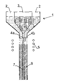
As shown in Fig. 1, a fiber with a core and a
cladding may be grown by using a crucible 1 with two con-
centric compartments 2, 3 containing the raw materials with
different concentrations and/or different types of dopants.
Instead of a single nozzle there are two concentric micro-
nozzles 4a, 4b at the bottom of two concentric crucible
compartments 2, 3. The two materials from the concentric
compartments 2, 3 are co-extruded (or co-pulled) and crys-
tallized under control of a heater 5, such that the mate-
rial from the outer compartment 2 forms the cladding 6
while the material from the inner compartment 3 forms the
core 7.
Crystal fiber with a waveguide through ion implantation
A further alternative to create a waveguide
in an electro-optical fiber - or in bulk material - is by
CA 02671587 2009-06-04
WO 2008/077256 PCT/CH2006/000735
8
means of ion implantation. It has been reported that a
waveguide in bulk BGO can be generated by implantation of
He+ ions [Ref. 10, 11]. The ion implantation produced an
index increase of about 1%-20. With this method, the fi-
bet may serve as a "substrate" and a waveguiding core is
created therein by irradiation with suitable ions.
Crystal fiber with a laser-written waveguide
Still another alternative to write a
waveguide is irradiation with laser light, in particular
short laser pulses. It is well-known that single-mode
waveguides can be created in fused silica and other glas-
ses by exposing the intended waveguide region with pico
or femtosecond laser pulses [Ref. 12]. Light-induced re-
fractive index changes can be created in electro-optical
materials as well, particularly when appropriately doped.
Persistent refractive index changes in undoped and chro-
mium doped BGO were reported [Ref. 13]. Hence, by expos-
ing the inner part of the material of the fiber to suffi-
ciently strong laser pulses allows to form a waveguiding
fiber core.
4. Polarimetric detection
Fig. 2 shows a set-up with a polarimetric detection
scheme using an electro-optical sensing fiber as de-
scribed above. Advantageously, a light source 10 of low
coherence is used (for example a light emitting diode or
a superluminescent diode (SLD)). In case of an SLD the
light is preferably depolarized in a fiber depolarizer
(not shown). An optical feed fiber 11 brings the light
from the source 10 to the electro-optical sensing fiber
12. Depending on the type of light source 10 and the di-
ameter of the electro-optical fiber 12, the feed fiber 11
may be multi-mode fiber, a single-mode fiber or a polari-
zation maintaining single-mode fiber.
After collimation in a collimator 13 the
light is polarized in polarizer 14 and coupled via a col-
CA 02671587 2009-06-04
WO 2008/077256 PCT/CH2006/000735
9
limator 15 into the sensing fiber 12. The polarizer 14 is
aligned at 45 to the electro-optical axes of the crys-
talline sensing fiber 12. The transmitted light exiting
from the sensing fiber 12 is again collimated in a colli-
mator 16 and then split in two channels by means of a
beam splitter 17. In case of-relatively thick sensing fi-
bers the collimators 15 and 16 may be omitted (case with
collimated beam in fiber). One of the two exit channels
contains a quarter-wave plate (k/4) 18 and a polarizer
19, the other channel only a polarizer 20. The wave plate
axes of the quarter-wave plate 18 are aligned parallel to
the electro-optical axes of the sensing fiber 12. The po-
larizers 19, 20 are aligned at 45 to the electro-optical
axes of the sensing fiber 12. Two multimode fibers 21a,
22a bring the light back to two photo detectors 21b, 22b.
The quadrature signals in the two channels
measured by the photodiodes 23, 24 are given by (see also
Ref. 1):
Channel 1 (with wave-plate 18):
Il = (1/2) Ip [1 + cos (I' - 7c/2) ] (1)
Il = (1/2) Ip [1 - sin F] (2)
Channel 2:
12 = (1/2) Ip [1 + cos I'] (3)
Ip is proportional to the light intensity.
For simplicity it is assumed that the fringe visibility
is equal to unity. I' is the electro-optical phase retar-
dation (Pockels effect) and varies with the applied volt-
age V according to:
I'=a (V / V.) (4)
Here V,n is the so-called half wave voltage:
Vn = X / (2 r n3) (5)
where X is the wavelength, r the relevant
electro-optical coefficient for the longitudinal Pockels
effect (r63 (= r41) in BGO) and n the refractive index of
the electro-optical fiber. The half wave-voltage of BGO
at 800 nm is about 41 kV [Ref. 5]. Since the applied
voltage is typically up to several hundred kilovolts, the
CA 02671587 2009-06-04
WO 2008/077256 PCT/CH2006/000735
signals Il and 12 go through several periods between two
extreme values of the applied voltage. However, the two
quadrature signals I1, 12 can be processed in such a way
that the waveform of the applied voltage is reconstructed
5 [Ref. 14].
Fig. 3 shows a set-up where the fiber is op-
erated in reflectiori using a mirro'r 28 at the end of
sensing fiber 12. This arrangement of the optical compo-
nents is equivalent to the one in Fig. lb of Ref. 1. Com-
10 pared to Fig. 1 the sensitivity is doubled (the halve-
wave voltage is lower by a factor of 2).
4.4 Interferometric detection
Fig. 4 shows a configuration employing a de-
tection technique adapted from fiber-optic gyroscopes
[Ref. 151 and interferometric current sensors, see
EP 1 154 278. The detection of the large electro-optical
phase shifts r(up to several multiples of n) requires
some adaptation of the signal processing not described in
Ref 15 and EP 1 154 278, however.
The set-up of Fig. 4 comprises a polarizing
beam splitter and phase modulator 23 that has two paral-
lel polarized outputs, the relative phase of which can be
changed by means of an applied electric voltage from a
signal processor 24. One output is led directly, and the
other via a 90 splice 25, to a polarization-maintaining
fiber coupler 26. From there, the two orthogonally polar-
ized waves are transmitted over a polarization maintain-
ing feed fiber 11, to a 45 Faraday rotator 27, i.e. a
non-reciprocal polarization rotator, from where they are
coupled into sensing fiber 12. A mirror 28 at the end of
sensing fiber 12 projects the waves back through sensing
fiber 12, Faraday rotator 27 (where the beams are rotated
by another 45 ), feed fiber 11 and fiber coupler 26. The
light waves pass through phase modulator 23 and are fed
to a photo detector 29.
CA 02671587 2009-06-04
WO 2008/077256 PCT/CH2006/000735
11
The non-reciprocal optical phase modulator 23
produces a periodic phase shift cpm =4Pm sin wmt with an
amplitude (Dm and an angular frequency com = 2lzvmt. The
modulation frequency vm is preferably chosen as vm =.
l/(2T) (or, equivalently, (om =a/T), where T is the
roundtrip time of the light in the optical circuit, i.e.
the time it takes the light exiting from modulator 23 to
return thereto. The modulation amplitude (Dm (for a given
modulator drive voltage) is then at a maximum.
The detected signal is given by
I = Io (1+ cos Dep) (6)
with Acp = cDm + I' (7)
Using Bessel functions the signal I can then
be expressed as
-==1+ J~~4Dj+2YJ,k(Om~os2kcomt~cas~is+
It~ C x~
..
+[2 ZJ z,('D.}cas(2k-1}wmt1sinOs
(8)
with os = F.
If only the DC term and the lst and 2nd har-
monics (frequencies t.)m, 2(om) are considered, the signal
can be written as
I Io [ 1 + JO ((Dm) + 2J2 (cDm) c o s (2comt) cos I' +...
+ 2J1 ((Dm) cos ((omt) sin I' + ... (9)
For a given value of the modulation amplitude
(Dm the amplitudes of the lst and 2nd harmonics vary in
proportion to sin I' and cos r, respectively, i.e. there
are again two quadrature signals. The waveform of the ap-
plied voltage can be reconstructed from these two signals
in the same way as it is done in the polarimetric scheme.
Preferably, (Dm is chosen such that the two harmonics have
the same amplitude, i.e. Jl((Dm) = J2((Dm). This is the
case for (Dm = 2.58 rad. Another preferred value of (Dm is
1.84 rad where J1((Dm) is'at its maximum. Alternatively,
(Dm may be chosen arbitrarily and the harmonics amplitudes
may be properly normalized by the signal processor.
CA 02671587 2009-06-04
WO 2008/077256 PCT/CH2006/000735
12
The configuration in Fig. 5 is the same as in
Fig. 4 apart from the fact that the electro-optical sens-
ing fiber 12 is separated from the Faraday rotator 27 by
two sections of polarization-maintaining (pm) fiber 30a,
30b. The separation may be advantageous in the practical
implementation of the sensor. The axes of the two pm fi-
ber sections are at 45 with respect to axes of the pm
feed fiber 11 before the rotator. There are two pm sec-
tions with a 90 -splice 31 in between in order to keep to
total optical path imbalance at zero (see EP 1 154 278).
Fig. 6 shows a set-up with two sections of
electro-optical sensing fiber 12a, 12b. The electro-
optical axes of the two sections 12a, 12b have a
90 angular offset and the directions 32a, 32b of the po-
lar crystal axes in the fiber 12a, 12b are anti-parallel.
This configuration is advantageous if fibers with intrin-
sic birefringence are used (crystal classes 6m2 and 2mm)
as the intrinsic (i.e. field-independent) birefringent
phase retardations in the two sections cancel each other.
In contrast the electro-optical phase shifts add to each
other.
As further alternatives the electro-optical
fibers(s) could be part of a loop mirror configuration or
a Sagnac configuration.
References
1. EP 0 682 261.
2. P. P. Chavez et al., IEEE Transactions on Power de-
livery 17, 362, 2002. .
3. D. H. Yoon et al., J. Crystal Growth 142, 339, 1994.
4. J. B. Shim et al, J. Applied Physics 93, 5131, 2003.
5. P. A. Williams et al., Applied Optics 35, 3562,
1996.
6. Y. Wang et al., in Proceedings of SPIE, vol. 5724,
42, 2005.
CA 02671587 2009-06-04
WO 2008/077256 PCT/CH2006/000735
13
7. T. Flaim et al., SPIE Proceedings on Optical Systems
Design, Advances in Optical Thin Films, Vol. 5250,
423, 2003.
B. C. Lu et al., J. Matr. Chem., 13, 2189, 2003.
9. S. G. Raymond et al., Radiation Measurements 23,
195, 1994.
10. S. M. Mahdavi et al, J. of Physics D: Applied Phys-
ics 22, 1354, 1989.
11. S. M. Mahdavi et al, Nuclear Instruments and Meth-
ods in Physics Research B65, 251, 1992.
12. K. Miura et al., Appl. Physics Letters 71, 3329,
1997.
13. J. S. McCullough et al., Journal of Applied Physics
90, 6022, 2001.
14. US patent 4 904 931, Feb. 27, 1990.
15. "The fiber-optic gyroscope", Herve Lefevre, Artech
House, Boston, London, 1993.
16. EP 1 154 278.
CA 02671587 2009-06-04
WO 2008/077256 PCT/CH2006/000735
14
List of Reference Numerals
1: crucible
2, 3: crucible compartments
4a, 4b: nozzles
5: heater
6: cladding
7: core
10: light source
11: feed fiber
12, 12a, 12b: sensing fiber
13: collimator
14: polarizer
15: collimator
16: collimator
17: beam splitter
18: quarter-wave plate
19: polarizer
20: polarizer
21a, 22a: multimode fibers
21b, 22b: photo detectors
23: beam splitter and phase modulator
24: signal processor
25: 90 splice
26: fiber coupler
27: Faraday rotator
28: mirror
29: photo detector
30a, 30b: polarization maintaining fiber
3o 31: 90 splice
32a, 32b: directions of the polar crystal axes.