Note: Descriptions are shown in the official language in which they were submitted.
CA 02672177 2009-06-08
1
DESCRIPTION
GAN EPITAXIAL SUBSTRATE, SEMICONDUCTOR DEVICE AND
METHODS FOR MANUFACTURING GAN EPITAXIAL SUBSTRATE AND
SEMICONDUCTOR DEVICE
Technical Field
[0001] The present invention relates to GaN epitaxial wafers and
semiconductor devices, and to methods of manufacturing GaN epitaxial wafers
and semiconductor devices.
Background Art
[0002] In order to improve light-emitting efficiency and other
microelectronic element properties in the fabrication of semiconductor devices
such as LEDs, monocrystalline GaN wafers have conventionally been
employed. The below-referenced Patent Document 1, for example, discloses a
method of producing a wafer of GaN single crystal by growing a ZnO layer
onto a substrate of a high-quality material such as sapphire, and thereafter
changing the crystallographic polarity of the ZnO layer and growing on it a
GaN single crystal and then dissolving off the ZnO layer.
Patent Document 1: Japanese Unexamined Pat. App. Pub. No. 2004-284831
Disclosure of Invention
Problem Invention Is to Solve
[0003] When monocrystalline GaN wafers are employed to attempt to
fabricate semiconductor devices, however, the following problem occurs.
Namely, in the process of growing epitaxial layers onto single-crystal wafers
CA 02672177 2009-06-08
2
and in the process of singulating the semiconductor devices after epitaxial-
layer formation, cracks are likely to occur in the epitaxial layers and single-
crystal wafers. In employing single-crystal wafers to fabricate semiconductor
devices, the occurrence of faults is thus frequent, such that production
yields
have not necessarily been high.
[0004] An object of the present invention, brought about taking the above
into consideration, is to make available= GaN epitaxial wafers designed to
improve production yields, as well as semiconductor devices utilizing such
GaN epitaxial wafers, and methods of manufacturing such GaN epitaxial
wafers and semiconductor devices.
Means for Resol ving the Problem
[0005] In order to achieve the above object, a GaN epitaxial wafer of the
present invention is characterized in including: a first GaN layer formation
step of epitaxially growing a first GaN layer onto a substrate; a pit
formation
step, following the first GaN layer formation step, of forming pits in the
front
side of the substrate; and a second GaN layer formation step, following the
pit-
formation step, of epitaxially growing a second GaN layer onto the first GaN
layer.
[0006] According to the foregoing manufacturing method, forming pits in
the front side of the substrate after epitaxially growing a first GaN layer
onto
the substrate alters the growth direction of the first GaN layer in the
proximity of the pits. Because the first GaN layer growth direction in the
other regions does not alter, areas appear where the growth direction differs
CA 02672177 2009-06-08
3
from the growth direction that the first GaN layer epitaxially grown at the
beginning possesses, bringing about a state in which zones having a plurality
of growth directions exist within the first GaN layer. When the second GaN
layer is thereafter epitaxially grown onto the first GaN layer having a
plurality of growth directions, the GaN layer where the growth direction
differs grows as different crystal, whereby a GaN epitaxial wafer having a
polycrystalline GaN layer is fabricated.
[0007] The present inventors, capping intensive research efforts, discovered
that utilizing GaN epitaxial wafers obtained by the present manufacturing
method to fabricate semiconductor devices made it possible to reduce the
above-described occurrence of cracking in the epitaxial layers and in the
wafers, enabling improvement in production yields in the fabrication of
semiconductor devices to be realized.
[0008] A GaN epitaxial wafer manufacturing method of the present
invention may be conditioned by having a mask-layer formation step, prior to
the first GaN layer formation step, of patterning a mask layer onto the front
side of the substrate.
[0009] A GaN epitaxial wafer manufacturing method of the present
invention may also be conditioned by the substrate being constituted by a
single layer. In that case, in the pit formation step the pits are formed onto
the single-layer substrate.
[0010] The method alternatively may be conditioned by the substrate being
constituted by a plurality of layers, wherein in the pit formation step the
pits
CA 02672177 2009-06-08
4
are formed on the uppermost layer of the substrate. According to these terms,
the materials that may be selected for the substrate multiply. GaN epitaxial
wafers involving the present invention can therefore be fabricated under
broader-ranging production requisites.
[0011] In a semiconductor device manufacturing method of the present
invention, included are: a first GaN layer formation step of epitaxially
growing a first GaN layer onto a substrate; a pit formation step, following
the
first GaN layer formation step, of forming pits in the front side of the
substrate; a second GaN layer formation step, following the pit-formation
step,
of epitaxially growing a second GaN layer onto the first GaN layer to
fabricate
a GaN epitaxial wafer; and a device manufacturing step of utilizing the GaN
epitaxial wafer to fabricate semiconductor devices.
[0012] In this implementation, forming pits in the front side of the substrate
after growing a first GaN layer onto the substrate alters the growth direction
of the first GaN layer in the proximity of the pits. Because the first GaN
layer
growth direction in the other regions does not alter, areas appear having a
growth direction that differs from the growth direction of the first GaN layer
epitaxially grown at the beginning, bringing about a state in which zones that
possess a plurality of growth directions exist within the first GaN layer.
Utilizing to fabricate semiconductor devices the GaN epitaxial wafer obtained
by thereafter epitaxially growing the second GaN layer onto the first GaN
layer having a plurality of growth directions makes it possible to reduce
CA 02672177 2009-06-08
incidents of cracking in fabricating the semiconductor devices, enabling
improvement in production yields to be realized.
[0013] A semiconductor device manufacturing method of the present
invention may also include a mask-layer formation step, prior to the first GaN
5 layer formation step, of patterning a mask layer onto the front side of the
substrate.
[0014] In a semiconductor device manufacturing method of the =present
invention, the substrate may be constituted by a single layer.
[0015] A semiconductor device manufacturing method of the present
invention alternatively may be conditioned by the substrate being constituted
by a plurality of layers, wherein in the pit formation step the pits are
formed
on the uppermost layer of the substrate.
-- - - -
[0016 Furthermore, a semiconductor device manufacturing method of the
present invention may be conditioned by, for the device manufacturing step,
utilizing to fabricate the semiconductor devices a GaN wafer obtained by
removing the substrate from the GaN epitaxial wafer. Not using the substrate
in the semiconductor devices lessens the restrictions on the material selected
for the substrate, making it possible to employ a wider range of materials for
the substrate. What is more, the fact that in the semiconductor devices only
layers composed of polycrystalline GaN laminae are utilized enables
semiconductor devices of superior device properties to be obtained, which can
serve to further improve production yields.
CA 02672177 2009-06-08
6
[00171 A GaN epitaxial wafer of the present invention is characterized in
being furnished with a substrate having pits in the major surface, and a
polycrystalline GaN layer layered onto the major surface. The fact that the
GaN layer laminated onto the major surface of the substrate is polycrystalline
makes it possible to minimize the occurrence of cracking in semiconductor
device fabrication, which can serve to further improve production yields.
[00181 A GaN epitaxial wafer of the present invention also may be furnished
with a mask layer, disposed in between the substrate and the polycrystalline
GaN layer.
[00191 A GaN epitaxial wafer of the present invention may also be
conditioned by the substrate being constituted by a single layer.
[00201 A GaN epitaxial wafer of the present invention alternatively may be
conditioned by the substrate being constituted by a plurality of layers, and
therein by having the pits in the uppermost layer of the substrate.
[0021] Semiconductor devices of the present invention are characterized by
having a substrate that has pits in its major surface, a GaN epitaxial wafer
that has a polycrystalline GaN layer layered onto the major surface, and a
semiconductor layer layered onto the polycrystalline GaN layer on the GaN
epitaxial wafer. Accordingly, the fact that the GaN layer laminated onto the
major surface of the substrate is polycrystalline minimizes incidents of
cracking during semiconductor device fabrication, thus serving to improve
production yields.
CA 02672177 2009-06-08
7
Effects of the In ven tion
[0022) The present invention makes available GaN epitaxial wafers serving
to improve production yields, and also affords semiconductor devices utilizing
the GaN epitaxial wafers, and methods of manufacturing the GaN epitaxial
wafers and the semiconductor devices.
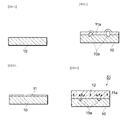
[00231 Fig. lA is diagram for illustrating a method of manufacturing a GaN
epitaxial wafer 51 involving Embodying Mode 1 of the present invention.
Fig. 1B is diagram for illustrating a method of manufacturing a GaN
epitaxial wafer 51 involving Embodying Mode 1 of the present invention.
Fig. 1C is diagram for illustrating a method of manufacturing a GaN
epitaxial wafer 51 involving Embodying Mode 1 of the present invention.
Fig. 1D is diagram for illustrating a method of manufacturing a GaN
epitaxial wafer 51 involving Embodying Mode 1 of the present invention.
Fig. 2A is a diagram schematically illustrating a peak obtained when
a conventional example of a monocrystalline GaN wafer 50 and a GaN
epitaxial wafer 51 involving Embodying Mode 1 of the present invention were
XRD analyzed.
Fig. 2B is a diagram schematically illustrating peaks obtained when
a conventional example of a monocrystalline GaN wafer 50 and a GaN
epitaxial wafer 51 involving Embodying Mode 1 of the present invention were
XRD analyzed.
Fig. 3A is diagram for illustrating a method of manufacturing a GaN
epitaxial wafer 52 involving Embodying Mode 2 of the present invention.
CA 02672177 2009-06-08
8
Fig. 3B is diagram for illustrating a method of manufacturing a GaN
epitaxial wafer 52 involving Embodying Mode 2 of the present invention.
Fig. 3C is diagram for illustrating a method of manufacturing a GaN
epitaxial wafer 52 involving Embodying Mode 2 of the present invention.
Fig. 3D is diagram for illustrating a method of manufacturing a GaN
epitaxial wafer 52 involving Embodying Mode 2 of the present invention.
Fig. 4 is a diagram showing a pattern for patterning with an Si02
film, employed in methods of the present invention of manufacturing a GaN
epitaxial wafer 52 involving Embodying Mode 2, and GaN epitaxial wafer 54
involving Embodying Mode 4
Fig. 5A is diagram for illustrating a method of manufacturing a GaN
epitaxial wafer 53 involving Embodying Mode 3 of the present invention.
Fig. 5B is diagram for illustrating a method of manufacturing a GaN
epitaxial wafer 53 involving Embodying Mode 3 of the present invention.
Fig. 5C is diagram for illustrating a method of manufacturing a GaN
epitaxial wafer 53 involving Embodying Mode 3 of the present invention.
Fig. 5D is diagram for illustrating a method of manufacturing a GaN
epitaxial wafer 53 involving Embodying Mode 3 of the present invention.
Fig. 6A is diagram for illustrating a method of manufacturing a GaN
epitaxial wafer 54 involving Embodying Mode 4 of the present invention.
Fig. 6B is diagram for illustrating a method of manufacturing a GaN
epitaxial wafer 54 involving Embodying Mode 4 of the present invention.
CA 02672177 2009-06-08
9
Fig. 6C is diagram for illustrating a method of manufacturing ~ GaN
epitaxial wafer 54 involving Embodying Mode 4 of the present invention.
Fig. 6D is diagram for illustrating a method of manufacturing a GaN
epitaxial wafer 54 involving Embodying Mode 4 of the present invention.
Fig. 7 is a diagram of a semiconductor device 110 involving
Embodying Mode 5 of the present invention.
Fig. 8A is a diagram of a semiconductor device 120 involving
Embodying Mode 6 of the present invention.
Fig. 8B is a diagram of a semiconductor device 120 involving
Embodying Mode 6 of the present invention.
Fig. 9 is a diagram of a semiconductor device 130 involving
Embodying Mode 7 of the present invention.
Fig. 10 is a diagram of a semiconductor device 140 involving
Embodying Mode 8 of the present invention.
Fig. 11 is a diagram of a semiconductor device 150 involving
Embodying Mode 9 of the present invention.
Fig. 12 is a diagram illustrating points for analyzing diffraction
patterns from a GaN wafer in an XRD determination.
Fig. 13 is an example of an XRD pattern recorded in the XRD
determination at one of the analysis points.
[0024] Legend
1: GaN wafer
10, 20, 30A 40A: substrate
CA 02672177 2009-06-08
51, 52, 53, 54: GaN epitaxial wafer
110: semiconductor device (LED)
120: semiconductor device (LD)
130: semiconductor device (HEMT)
5 140: semiconductor device (Schottky diode)
150: semiconductor device (vertical MIS transistor)
[0025] Best Mode for Carrying Out the Invention
Hereinafter, referring to the accompanying drawings, an explanation
of embodiments of the present invention will be made in detail. It should be
10 understood that in describing the drawings, with the same reference marks
being used for identical or equivalent features, reduplicating description
will
be omitted.
Embodying Mode 1
[00261 Fig. 1 is diagrams for illustrating a method of manufacturing a GaN
epitaxial wafer 51 involving Embodying Mode 1 of the present invention.
Included by a method, involving the present embodying mode, of
manufacturing a GaN epitaxial wafer 50 are:
(1) As indicated in Figs. 1A and 1B, a first GaN layer formation step of
epitaxially growing a first GaN layer 11 onto a substrate 10;
(2) As indicated in Fig. 1C, a pit formation step, following the first GaN
layer
formation step, of forming pits 10a in the front side of the substrate 10; and
CA 02672177 2009-06-08
11
(3) As indicated in Figs. 1C and 1D, a second GaN layer growth step, following
the pit-formation step, of epitaxially growing a second GaN layer 12 onto
the first GaN layer lla, having been transformed by the pit formation step.
In the following, each of the foregoing manufacturing process steps will be
explained in detail.
[0027] To begin with, a single-crystal substrate 10, represented in Fig. 1A,
is
prepared. InP, GaAs, GaP, GaN, AIN or a like material is preferable for the
substrate 10. These semiconductor materials facilitate the formation of pits
in
the pit formation step, making them ideally suited as substrates involving the
present embodying mode.
[0028] Next, as the first GaN layer formation step, a first GaN layer 11 is
epitaxially grown onto the substrate 10, as indicated in Fig. 1B. For the
method of growing the first GaN layer 11, it is for example by a technique
such
as hydride or halide vapor phase epitaxy (HVPE). The thickness is
approximately 1 ,pnn.
[0029] Subsequently, as the pit formation step, pits l0a are formed in the
front side of the substrate 10, as indicated in Fig. 1C. The means whereby the
pits are formed may be, to cite examples, a method whereby the substrate 10
to be provided with the first GaN layer 11 thereon is taken out of the growth
reactor and etched with NH3 or a like solution that is corrosive, a method
whereby the substrate is etched within the growth reactor using HCl gas or
NH3 gas, or a method whereby the substrate is heated. A specific example is a
method whereby HCl gas is flowed under a temperature of 800 C to carry out
CA 02672177 2009-06-08
12
etching. These operations form pits 10a in the front side of the substrate 10,
as indicated in Fig. 1C, and at the same time the first GaN layer itself, by
the
etching and heating, turns into a first GaN layer lla in which the epitaxial
layer-especially the areas where it covers the front side of the pits l0a-has
been spot-transformed.
[0030] When GaN further grows epitaxially onto the front side of the first
GaN layer lla, a second GaN layer 12, as illustrated in Fig. 1D, forms. As the
second GaN layer formation step, in Fig. 1D, a second GaN layer 12 is
epitaxially grown onto the front side of the first GaN layer lla. The second
GaN layer 12 is thereby formed as a polycrystalline layer. In Fig. 1D the
arrows within the first GaN layer lla and second GaN layer 12 schematically
represent crystal-growth directions. In the GaN epitaxial wafer thus obtained,
pits l0a in between the substrate 10 and the first GaN layer lla, as indicated
in Fig. 1D, will remain.
[0031] The crystal structure of the GaN epitaxial wafer 51 obtained in the
manner set forth above will now be described, in comparison with a
conventional, monocrystalline GaN wafer. Fig. 2 is diagrams schematically
illustrating peaks obtained when a conventional example of a monocrystalline
GaN wafer 50 and a GaN epitaxial wafer 51 involving Embodying Mode 1 of
the present invention were XRD analyzed. Fig. 2A is the instance with the
monocrystalline GaN wafer 50, and Fig. 2B is the instance with the GaN
epitaxial wafer 51 obtained according to Embodying Mode 1. Included in each
drawing is a figure schematically representing the surface of the crystal
wafer,
CA 02672177 2009-06-08
13
a sectional view (with the arrows indicating crystal-growth directions)
through
the center-line portion of the figure, and an example of an x-ray diffraction
pattern obtained when a beam of x-rays was directed onto the crystal.
[0032] Given that the monocrystalline GaN wafer 50 is monocrystalline, its
growth directions also, as indicated in Fig. 2A (the arrows in the figure),
are
essentially in a singular orientation. When an x-ray beam L strikes the front
side of the crystal, the beam L is reflected by a crystallographic plane
possessing the singularly oriented growth direction (crystal orientation), and
therefore a singular peak is obtained. In the case of a GaN epitaxial wafer 51
involving Embodying Mode 1, however, as indicated in Fig. 2B, grain
boundaries (or otherwise, interfaces that are like low-angle grain boundaries)
are present, and along the grain boundaries the crystal growth direction
changes. When an x-ray beam L strikes the crystal in the vicinity of a grain
boundary, because the beam L is reflected by a plurality of (two)
crystallographic planes, the crest in the XRD pattern obtained is split into a
plurality of (two) peaks. Thus, when an x-ray beam is directed onto the
polycrystal wafer, owing to the fact that the crystal growth directions each
differ, split peaks are seen.
[0033] The present inventors discovered that utilizing a GaN epitaxial wafer
composed of a GaN polycrystal in which split peaks are characterized in its
XRD pattern, as sketched in Fig. 2B, to fabricate semiconductor devices makes
it possible to reduce the incidence of cracking during semiconductor device
fabrication, enabling improved production yields to be realized, by comparison
CA 02672177 2009-06-08
14
with the situation in which devices are fabricated using a GaN single crystal
like that represented in Fig. 2A. The causative factors behind this are
believed to be as follows.
[0034] To begin with, strain can be considered to be a cause of cracking.
Specifically, when semiconductor devices are fabricated using a
monocrystalline GaN wafer as the foundation, epitaxial layers whose
composition differs, or whose impurity level differs, from that of GaN are
formed onto the substrate. The lattice constants and thermal expansion
coefficients in the monocrystalline GaN wafer and the epitaxial layers
therefore do not agree, owing to which in the midst of formation or following
formation of the epitaxial layer, strain occurs at the interface between the
wafer and epitaxial layers. The strain causes cracking.
[0035] Furthermore, another cause of cracking is believed to be that when
thermal or mechanical external forces are imparted in the course of cooling
the
epitaxial layers after they have been formed-and further, during post-
formation back side processing of the epitaxial layers and in the dicing
process-cracking is likely to occur.
[0036] Yet in instances in which the GaN wafer has grain boundaries, as in
the present embodying mode, the grain boundaries are believed to act as a
cushioning element (function as a buffer). Specifically, it is believed that a
phenomenon obtains whereby for example when strain is produced in a GaN
wafer, dislocations multiply at the grain boundaries, where crystal defects
are
largely incorporated, mitigating the strain, or the crystal slips along the
CA 02672177 2009-06-08
crystal defects, mitigating the strain. Accordingly, fabricating semiconductor
devices utilizing a GaN epitaxial wafer constituted by polycrystal GaN in the
manner of the present embodying mode is thought to make it possible to
obtain the devices at, with a low incidence of cracking, high production
yields.
5 Embodying Mode 2
[0037] Fig. 3 is diagrams for illustrating a method of manufacturing a GaN
epitaxial wafer 52 involving Embodying Mode 2 of the present invention.
Included by a method, involving the present embodying mode, of
manufacturing a GaN epitaxial wafer 52 are:
10 (1) As indicated in Fig. 3A, a mask-layer formation step of patterning a
mask
layer 21 onto the front side of a substrate 20;
(2) As indicated in Fig. 3B, a first GaN layer formation step of epitaxially
growing a first GaN layer 22 onto the front side of the substrate 20 on
which the mask layer 21 has been formed;
15 (3) As indicated in Fig. 3C a pit formation step, following the first GaN
layer
formation step, of forming pits 20a in the front side of the substrate 20; and
(4) As indicated in Figs. 3C and 3D, a second GaN layer formation step,
following the pit-formation step, of forming a second GaN layer 23 onto the
mask layer 21a and first GaN layer 22a, having been transformed by the
pit formation step.
In the following, each of the foregoing manufacturing process steps will be
explained in detail while making a comparison with Embodying Mode 1.
CA 02672177 2009-06-08
16
[0038] A method, involving Embodying Mode 2, of manufacturing a GaN
epitaxial wafer 52 differs compared with Embodying Mode 1, in the respect
that as a mask-layer formation step a mask layer 21 is patterned onto the
front side of the substrate 20. As the mask layer 21 an Si02 film, for
example,
is ideally suitable. And the method whereby the mask layer is patterned may
be a general formation technique. As a specific example, an Si02 film may be
applied over the entire surface, after which a mask layer 21, as indicated in
Fig. 4, is obtained by performing a photolithographic process in a manner such
that squares 60, 5Fm to a side, form a matrix array at a 5 pm spacing 60a.
[0039] Thus, with an implementation in which the mask layer 21 is formed
on the front side of the substrate 20, when pits 20a are formed in the front
side
of the substrate 20, as illustrated in Fig. 3C, with the first GaN layer 22
spot-
transforming over the pits 20a, in a like manner as in Embodying Mode 1, the
growth directions in those areas change, resulting in a first GaN layer 22a
containing grain boundaries. At the same time, as the pits are formed the
mask layer 21 inclines, as represented in Fig. 3C, turning into a displaced
mask layer 21a. Onto a mask layer 21a of such form, in the succeeding step of
creating the second GaN layer 23, the GaN grows epitaxially in directions that
differ from the initial growth direction. A GaN epitaxial wafer incorporating
a
second GaN layer 23 that is a polycrystalline layer can thereby be produced.
[0040] In Embodying Mode 2, similarly as in Embodying Mode 1, a GaN
epitaxial wafer 52 incorporating a polycrystalline GaN layer can be produced
as described above. Then utilizing the GaN epitaxial wafer 52 to fabricate
CA 02672177 2009-06-08
17
semiconductor devices enables the devices to be obtained with minimal
occurrence of cracks, for high production yields.
Embodying Mode 3
[0041] Fig. 5 is diagrams for illustrating a method of manufacturing a GaN
epitaxial wafer 53 involving Embodying Mode 3 of the present invention.
Included by a method, involving the present embodying mode, of
manufacturing a GaN epitaxial wafer 53 are:
(1) As indicated in Figs. 5A and 5B, a first GaN layer formation step of
epitaxially growing a first GaN layer 32 onto the front side of a second
substrate layer 31 on a substrate 30A composed of two layers-a first
substrate layer 30 and the second substrate layer 31, on the front side of
the first substrate layer 30;
(2) As indicated in Fig. 5C, a pit formation step, following the first GaN
layer
formation step, of forming pits 31a in the front side of the second substrate
layer 31 (the uppermost layer of the substrate); and
(3) As indicated in Figs. 5C and 5D, a second GaN layer growth step, following
the pit-formation step, of epitaxially growing a second GaN layer 33 onto
the first GaN layer 32a, having been transformed by the pit formation step.
In the following, each of the foregoing manufacturing process steps will be
explained in detail while making a comparison with Embodying Mode 1 and
Embodying Mode 2.
[0042] A method, involving Embodying Mode 3, of manufacturing a GaN
epitaxial wafer 53 differs from Embodying Mode 1 and Embodying Mode 2 in
CA 02672177 2009-06-08
18
the respect that the substrate 30A is composed of a plurality of layers. With
an implementation in which the substrate 30A is made a plurality of layers, in
the pit formation step in the present embodying mode, the pits are formed in
the second substrate layer 31, which is the uppermost layer of the substrate.
As the semiconductor material utilized for the second substrate layer 31,
compounds such as InP, GaAs, GaP, GaN and A1N, which facilitate the forming
of pits in the pit formation step, are preferable. Also, in the present
embodying mode the material utilized as the first substrate layer 30 is not
limited to the just-mentioned InP, GaAs, GaP, GaN, AlN and the like;
materials such as sapphire substrates, for example, that do not corrode easily
under etching or a like process can be utilized. An example of a- specific
technique whereby the second substrate layer 31 is formed onto the first
substrate layer 30 is a method whereby a (0001) c-plane sapphire substrate
top is readied as the first substrate layer 30, onto which a GaN crystal layer
is
grown using the metalorganic chemical vapor deposition (MOCVD) technique
to form the second substrate layer 31.
[00431 In accordance with Embodying Mode 3 as just described, a GaN
epitaxial wafer 53 incorporating a polycrystalline GaN layer can be produced.
Then utilizing the GaN epitaxial wafer 53 to fabricate semiconductor devices
enables the devices to be obtained with minimal occurrence of cracks, for high
production yields. Furthermore, according to the present embodying mode,
the fact that the substrate 30A is made up of a plurality of layers increases
the
CA 02672177 2009-06-08
19
choice of materials utilized for substrate 30A, enabling the GaN epitaxial
wafer 53 to be produced under a broader range of manufacturing conditions.
Embodying Mode 4
[0044) Fig. 6 is diagrams for illustrating a method of manufacturing a GaN
epitaxial wafer 54 involving Embodying Mode 4 of the present invention.
Included by a method, involving the present embodying mode, of
manufacturing a GaN epitaxial wafer 54 are:
(1) As indicated in Fig. 6A, a mask-layer formation step of patterning a mask
layer 42 onto the front side of a substrate 40A composed of two layers-a
first substrate layer 40 and a second substrate layer 41 on the front side of
the first substrate layer 40;
(2) As indicated in Fig. 6B, a first GaN layer formation step of epitaxially
growing a first GaN layer 43 onto the front side of the second substrate
layer 41 on which the mask layer 42 has been formed;
(3) As indicated in Fig. 6C a pit formation step, following the first GaN
layer
formation step, of forming pits 41a in the front side of the second substrate
layer 41 (the uppermost layer of the substrate); and
(4) As indicated in Figs. 6C and 6D, a second GaN layer growth step, following
the pit-formation step, of epitaxially growing a second GaN layer 44 onto
the first GaN layer 43a, having been transformed by the pit formation step.
In the following, each of the foregoing manufacturing process steps will be
explained in detail while making a comparison with Embodying Mode 1
through Embodying Mode 3.
CA 02672177 2009-06-08
[0045] A method, involving Embodying Mode 4, of manufacturing a GaN
epitaxial wafer 54 is similar to Embodying Mode 3 in the respect that the
substrate 40A is made up of a plurality of layers.
The present embodying mode is further characterized in having, similar to
5 Embodying Mode 2, a mask-layer formation step, prior to the first GaN layer
growth step, of patterning a mask layer 42.
[0046] In accordance with Embodying Mode 4 as just described, a GaN
epitaxial wafer 54 incorporating a polycrystalline GaN layer can be produced.
Then utilizing the GaN epitaxial wafer 54 to fabricate semiconductor devices
10 enables the devices to be obtained with minimal occurrence of cracks, for
high
production yields. Furthermore, according to the present embodying mode,
the fact that the substrate 40A is made up of a plurality of layers increases
the
choice of materials utilized for substrate 40A, enabling the GaN epitaxial
wafer 54 to be produced under a broader range of manufacturing conditions.
15 [0047] The GaN epitaxial wafers 51 through 54 obtained according to
Embodying Mode 1 through Embodying Mode 4 can be utilized without
modification to fabricate semiconductor devices. Alternatively, as needed the
laminar part consisting of the first GaN layer and second GaN layer can be
separated from the substrate 10, 20, 30A or 40A and utilized as a
20 polycrystalline GaN wafer in the manufacture of semiconductor devices. When
a wafer obtained by separating the substrates 10, 20, 30A or 40A from GAN
epitaxial wafers 51 through 54 is used as the GAN wafer from which
CA 02672177 2009-06-08
21
semiconductor device with a high performance is made, because the device is
provided with only a layer composed of GAN.
[0048] In the following semiconductor-device embodying modes involving the
present invention, semiconductor devices utilizing polycrystalline GaN wafers
1, obtained by separating the substrates 10, 20, 30A and 40A from the GaN
epitaxial wafers 51 through 54 produced according to Embodying Mode 1
through Embodying Mode 4, will be described.
Embodying Mode 5
[0049] Fig. 7 is a diagram of a semiconductor device 110 involving
Embodying Mode 5 of the present invention. As shown in Fig. 7, the
semiconductor device 110 involving the present embodying mode is composed
of a semiconductor laminar structure in which are formed, in order on the
front side of a GaN wafer 1, an rrtype GaN layer 201, an n-type AlGaN layer
202, a light-emitting layer 203, a p-type AlGaN layer 204, and a p-type GaN
layer 205; a p-electrode 251 on the front side of the p-type GaN layer 206;
and
an n-electrode 252 on the back side of the GaN wafer 1. This semiconductor
device 110 functions as a light-emitting diode (LED).
[0050] The light-emitting layer 203 may be a multiquantum-well (MQW)
structure-for example, in which a bilaminar GaN-layer and Ino.2Gao.8N-layer
structure is stacked multi-tiered.
[0051) The semiconductor device 110 of the present embodying mode is
fabricated by the following method for example. To begin with, for the device
manufacturing step, the ntype GaN layer 201, the n-type AIGaN layer 202,
CA 02672177 2009-06-08
22
the light-emitting layer 203, the p-type AlGaN layer 204, and the p-type GaN
layer 205 are formed, in order, by MOCVD onto the front side of the GaN
wafer 1. Subsequently, the p-electrode 251, at a thickness of 100 nm, is
formed
onto the front side of the p-type GaN layer 205. Further, the n-electrode 252
is
formed on the back side of the GaN wafer 1, thereby yielding an LED-i.e.,
semiconductor device 110.
[0052] In accordance with Embodying Mode 5 as just described, utilizing a
polycrystalline-GaN-layer- incorporating GaN epitaxial wafer to fabricate a
semiconductor device makes it possible to produce a semiconductor device
(LED) in which cracking is minimal and the yield rate is superior.
Embodying Mode 6
[0053] Fig. 8 is diagrams of a semiconductor device 120 involving Embodying
Mode 6 of the present invention. As shown in Fig. 8B, the semiconductor
device 120 involving the present embodying mode is composed of a
semiconductor laminar structure in which are formed, in order on the front
side of a GaN wafer 1, an n-type GaN buffer layer 206, an n-type AlGaN
cladding layer 207, an n-type GaN optical waveguide layer 208, an active layer
209, an undoped InGaN deterioration-preventing layer 210, a p-type AlGaN
gap layer 211, a p-type GaN optical waveguide layer 212, a p-type AlGaN
cladding layer 213, and a p-type GaN contact layer 214; and further, a p-
electrode 251 on the front side of the p-type GaN contact layer 214, and an zr
electrode 252 on the back side of the GaN wafer. This semiconductor device
120 functions as a laser diode (LD).
CA 02672177 2009-06-08
23
[0054] The semiconductor device 120 of the present embodying mode is
fabricated by the following method for example. To begin with, for the device
manufacturing step, as shown in Fig. 8A the n-type GaN buffer layer 206, the
n-type AlGaN cladding layer 207, the n-type GaN optical waveguide layer 208,
the active layer 209, the undoped AIGaN deterioration-preventing layer 210,
the p-type AlGaN gap layer 211, the p-type GaN optical waveguide layer 212,
the p-type AlGaN cladding layer 213, and the p-type GaN contact layer 214 are
formed, in order, by MOCVD onto the front side of the GaN wafer 1. Next, an
Si02 film is formed across the entire front side of the p-type GaN contact
layer
214 by the CVD method and then is patterned photolithographically. Next, as
indicated in Fig. 8B a ridge 215 is formed by etching thickness-wise to a
predetermined depth into the p-type AlGaN cladding layer 213. The Si02 film
is thereafter cleared away, and then an Si02 insulating film 216 is formed
over
the entire wafer surface. Next, by formation of a resist pattern and by
etching,
the p-electrode 251 is formed onto the upper surface of the p-type GaN contact
layer alone. Thereafter forming the rrelectrode 252 on the back side yields an
LD-i.e., semiconductor device 120.
[0055] Here, to form the Si02 film methods such as vacuum deposition or
sputtering method may be employed, while etching of the Si02 film may be by
an RIE technique employing a fluorine-containing etchant gas.
[0056] In accordance with Embodying Mode 6 as just described, utilizing a
polycrystalline-GaN-layer- incorporating GaN epitaxial wafer to fabricate a
CA 02672177 2009-06-08
24
semiconductor device 120 makes it possible to produce a semiconductor device
(LD) 120 in which cracking is minimal and the yield rate is superior.
Embodying Mode 7
[0057] Fig. 9 is a diagram of a semiconductor device 130 involving
Embodying Mode 7 of the present invention. As shown in Fig. 9, the
semiconductor device 130 involving the present embodying mode is composed
of. an i-type GaN layer 221a and an itype AlGaN layer 221b formed, in order,
as an at least single-lamina III-nitride semiconductor layer 221 on the front
side of a GaN wafer 1; and further, on the front side of the itype AlGaN layer
221 b, a source electrode 253, a gate electrode 254, and a drain electrode
255.
This semiconductor device 130 functions as a high electron mobility transistor
(HEMT).
[0058] The semiconductor device 130 of the present embodying mode is
fabricated by the following method for example. For the device manufacturing
step, as shown in Fig. 9, the itype GaN layer 221a and the itype AIGaN layer
221b are grown onto the front side of the GaN wafer 1, after which the source
electrode 253 and drain electrode 255 are formed onto the i-type-A1GaN layer
221 b by photolithographic and lift-off processes, following which the gate
electrode 254 further is formed, yielding an HEMT-i.e., semiconductor device
130.
[0059] In accordance with Embodying Mode 7 as just described, utilizing a
polycrystalline-GaN-layer- incorporating GaN epitaxial wafer to fabricate a
CA 02672177 2009-06-08
semiconductor device 130 makes it possible to produce a semiconductor device
(HEMT) 130 in which cracking is minimal and the yield rate is superior.
Embodying Mode 8
[0060] Fig. 10 is a diagram of a semiconductor device 140 involving
5 Embodying Mode 8 of the present invention. As shown in Fig. 10, the
semiconductor device 140 involving the present embodying mode includes: an
n-type GaN layer 221 as an at least single-lamina III-nitride semiconductor
layer on the front side of a GaN wafer 1, and is furnished with an ohmic
electrode 256 on the back side of the GaN wafer 1. Further, a Schottky
10 electrode 257 is furnished on the front side of the n=type GaN layer 221.
This
semiconductor device 140 functions as a Schottky diode.
[0061] The semiconductor device 140 of the present embodying mode is
fabricated by the following method for example. For the device manufacturing
step, as shown in Fig. 10, the n--type GaN layer 221 is grown, by MOCVD,
15 onto the GaN wafer 1. Next the ohmic electrode 256 is formed across the
entire back side of the GaN wafer 1. Further, the Schottky electrode 257 is
formed onto the n-type GaN layer by photolithographic and lift-off processes.
By the above, a Schottky diode-i.e., semiconductor device 140-is obtained.
[0062] In accordance with Embodying Mode 8 as just described, utilizing a
20 polycrystalline-GaN-layer- incorporating GaN epitaxial wafer to fabricate a
semiconductor device 140 makes it possible to produce a semiconductor device
(Schottky diode) 140 in which cracking is minimal and the yield rate is
superior.
CA 02672177 2009-06-08
26
Embodying Mode 9
[0063] Fig. 11 is a diagram of a semiconductor device 150 involving
Embodying Mode 9 of the present invention. As shown in Fig. 11, in the
semiconductor device 150 involving the present embodying mode, an n-type
GaN layer 221c is formed as an at least single-lamina III-nitride
semiconductor layer 221 on the front side of a GaN wafer 1, and a p-type GaN
layer 221d and an n*-type GaN layer 221e are formed in regions occupying
part of the upper surface of the n-type GaN layer. Further furnished are: a
drain electrode 255 on the back side of the GaN wafer 1, a gate electrode 254
on the front side of the n--type GaN layer 221c, and a source electrode 253 on
the front side of the n+-type GaN layer 221e. This semiconductor device 150
functions as a vertical metal-insulator-semiconductor (MIS) transistor.
[0064] The semiconductor device 150 of the present embodying mode is
fabricated by the following method for example. For the device manufacturing
step, as shown in Fig. 11, the n-type GaN layer 221c is formed by MOCVD
onto the front side of a GaN wafer 1. Subsequently, by implantation of select
ions, the p-type GaN layer 221dand nf-type GaN layer 221e are in that order
formed in regions occupying part of the upper surface of the n-type GaN layer.
Next, an Si02 film is employed to protect the n-type GaN layer 221c, which is
then annealed to activate the implanted ions. By plasma-enhanced chemical
vapor deposition (P-CVD), an Si02 film is formed as an insulating film for the
vertical MIS; then by a photolithographic process and a select etching process
employing buffered hydrofluoric acid, a portion of the aforementioned vertical
CA 02672177 2009-06-08
27
MIS insulating film is etched, and by a lift-off process the source electrode
253
is formed on the front side of the n+-type GaN layer 221e. Next, by
photolithographic and lift-off processes the gate electrode 254 is formed onto
the vertical MIS insulating film. Further, the drain electrode 255 is formed
across the entire back side of the GaN wafer 1, yielding a vertical MIS
transistor-i.e., semiconductor device 150.
[00651 In accordance with Embodying Mode 9 as just described, utilizing a
polycrystalline-GaN-layer- incorporating GaN epitaxial wafer to fabricate a
semiconductor device 150 makes it possible to produce a semiconductor device
(vertical MIS transistor) 150 in which cracking is minimal and the yield rate
is
superior.
EMBODIMENTS
[00661 Below, with GaN epitaxial wafers, and semiconductor devices
fabricated based on semiconductor-device manufacturing methods, involving
the present invention as embodiment examples, and with semiconductor
devices fabricated employing conventional monocrystalline GaN wafers as
comparative examples, a further detailed description of the present invention
will be made, yet the present invention is not limited to the following
embodiment examples.
CA 02672177 2009-06-08
28
Production of Wafers Used in Erabodiment Examples and Comparative
Examples
Production of GaN Wafers Utilized in Embodiments 1 to 50 and Embodiments
AtoE
(0067) The GaN epitaxial wafer utilized in the method of above-described
Embodying Mode 4 was fabricated. To begin with, MOCVD was employed to
grow a GaN crystal layer (corresponding to the first GaN layer) 3lnn onto 2.5-
inch (Embodiments 1 to 50) as well as 3-inch (Embodiments A to E) (0001) c
plane sapphire wafers (corresponding to the first GaN layer formation step).
Thereafter the sapphire wafers onto which the GaN crystal layer had been
grown were taken out of the reactor, and an Si02 film was layered onto GaN
crystal layer and was patterned by a photolithographic process employing a
lattice pattern with 5-pm sized windows and a 5 pm linewidth (the
photographic negative of the mask pattern 60 depicted in Fig. 4). After that,
GaN crystal growth employing HVPE was carried out at 1000 C to a thickness
of approximately 1 pm onto the Si02 film. When the growth-bearing wafers
were withdrawn and examined, GaN crystal had grown partially, wherein
regions where GaN crystal had not grown could be observed in part. The
wafers were once again inserted into the HVPE reactor, where they were
etched by flowing an HCl gas at 800 C (corresponding to the pit formation
step), and then they were taken out of the reactor and underwent SEM
observation, whereupon part of the starting GaN crystal and the grown GaN
crystal had been etched, with inclined GaN crystal also being observed. The
CA 02672177 2009-06-08
29
wafers were once again inserted into the HVPE reactor, where at 1000 C GaN
crystal was grown onto them to a thickness of approximately 300 Pm
(corresponding to the second GaN layer formation step), after which the wafers
were taken out of the HVPE reactor. The above steps yielded GaN epitaxial
wafers.
[0068] Subsequently, among the GaN epitaxial wafers, the portion with a
layer consisting of GaN polycrystal were sliced from their sapphire substrates
to yield polycrystalline GaN wafers.
XRD Analysis
[0069] The XRD patterns of the polycrystalline GaN wafers obtained by the
method detailed above were recorded, and the number of sites with crystal-
peak divisions and the number of peaks were determined.
[0070] The method whereby the XRD patterns were determined will be
specifically set forth using Fig. 12. A double-crystal x-ray diffractometer
was
employed as the analyzer, and for the analysis parameters, the slit dimensions
were let be 500 pm length x 200 Inn width, the x-ray beam incident orientation
was let be along a<11-20> direction, and the diffraction plane was let be the
(0004) plane. Fig. 12 is a diagram illustrating points for analyzing
diffraction
patterns from the polycrystalline GaN wafers. Analysis points were thus
established in thirteen sites from the center of the GaN wafers at 10-mm
spacings along a <11-20> direction and along a <1-100> direction. The
diffraction patterns in these points were determined, and at each analysis
CA 02672177 2009-06-08
point the presence of divisions in the diffraction peaks and the number of
peaks were found.
[0071] Fig. 13 is an example of a diffraction pattern recorded at one of the
analysis points. From the presence of divisions and the number of peaks in
5 the thirteen places, thus obtained from the diffraction patterns recorded at
each analysis point, the split peak mean count was found by the following
procedure. To begin with, letting the number of analysis points where peak-
splitting arose (points where the peak count was 2 or more) be n sites (n
being
a whole number from 1 to 13) and the peak counts at the analysis points where
10 peak-splitting arose be respectively a1 to an, then the number found by the
following general formula (1)
split peak mean count = (a1 + . . . + an)/n (1)
was taken as the split peak mean count.
[0072] The aforedescribed numerical value was found for a plurality of
15 polycrystalline GaN wafers to distinguish wafers to be utilized in
Embodiments 1 to 50. Utilizing these polycrystalline GaN wafers of
Embodiments 1 to 50 (ten wafers for each embodiment, 500 wafers total),
semiconductor devices were fabricated based on each of the following
semiconductor-device manufacturing methods.
20 [0073] As the wafers utilized in the semiconductor devices of Embodiments A
through E, fifty polycrystalline GaN wafers of 3-inch size, and whose peak-
split occurrence sites were one site (n = 1) and whose peak split count in the
peak-split occurrence sites was 2 (making the split peak mean count 2) were
CA 02672177 2009-06-08
31
readied. Utilizing these, semiconductor devices were fabricated based on each
of the following semiconductor-device manufacturing methods.
Monocrystalline GaN wafers for Comparative Examples 1 through 5 and
Comparative Examples A through E
[0074] Monocrystalline GaN wafers of 2.5-inch size and 400-jrm thickness
were used for Comparative Examples 1 through 5, and wafers of 3-inch size
and 400-,um thickness for Comparative Examples A through E. These
monocrystalline GaN wafers were x-ray analyzed to determine their
diffraction patterns in the same manner as were the polycrystalline GaN
wafers utilized in the embodiments, whereat peak-splitting did not arise in
any of the analysis points.
Semiconductor Device Testing Method
1. Crack Test
[0075] The wafers divided into the respective embodiments / comparative
examples were observed under a differential interference microscope to check
for the presence of cracks. The observation zone was the entire surface of
each
wafer excluding a 5 mm periphery, and the observation magnification of the
objective lens was set to be 20X. In instances where cracks were discovered,
if
there were thirty or more cracks of 100 j.rm or greater length, the wafer was
considered to be "cracks present" and deemed a failure, and was not passed to
the succeeding stage.
[0076] The crack test was conducted two times in the step of manufacturing
each semiconductor device. The first time was after semiconductor layers
CA 02672177 2009-06-08
32
were grown onto the wafer (in Tables I through X setting forth the results,
entered as "cracking @ epi"), while the second time was after performing
processes including forming an electrode on the back side of the wafer
(entered
as "cracking @ back lap" in Tables I through X). In Tables I through X
presenting the results, the number of wafers deemed to be free of cracks
(qualifying wafers) is given.
2. Device Test
[0077] An evaluation concerning the device properties of each semiconductor
device fabricated in the semiconductor device manufacturing step was as
follows. To begin with, to characterize the device properties of the
semiconductor devices, corresponding to the comparative examples of each
semiconductor device, incorporating the monocrystalline GaN wafers,
determined in each case were, with their mean values and a being calculated:
for LEDs, emission intensity; for LDs, lasing lifespan; for HEMTs, Schottky
diodes, and vertical MIS transistors, "ON" resistance. On this basis the
device
properties of each of the semiconductor devices of the embodiments were
characterized, and those having results over the value [mean - o] for the
device properties of the comparative examples were taken to be qualifying.
With the devices incorporating the comparative examples, in the same way,
those having results over the value [mean - ol for the comparative-example
device properties were taken to be qualifying.
[0078] Using, among the numerical values obtained from the above-
described tests, the number of qualifying wafers in the two-times crack test
CA 02672177 2009-06-08
33
(the number given at "cracking @ back lap" in Tables I through X) and the
device-property test results (proportion of qualifying chips), the total yield
rate
was calculated employing the following general formula (2).
total _ count of wafers X proportion of device-property- (2)
yield qualifying in crack test qualifying chips (%)
[0079] Using the method described above, tests were conducted on the
following semiconductor-device embodiments and comparative examples.
Details of the method manufacturing, and the results of testing, the
semiconductor-devices are presented below.
Embodiments 1 to 10; Comparative Example 1
[0080] Embodiments 1 to 10 and Comparative Example 1 are LEDs being
semiconductor device 110 involving Embodying Mode 5 of the present
invention. The manufacturing method and testing method were as follows.
[0081] By MOCVD, a 5-pm thick n-type GaN layer, a 3-nm thick Ino.2Gao.$N
layer, a 60-nm thick Alo.2Gao.sN layer, and a 150-nm thick p-type GaN layer
were epitaxially grown, in that order, as an at least single-lamina III-
nitride
semiconductor layer onto a 2.5-inch size, 400-1rm thick polycrystalline GaN
wafer (in Comparative Example 1, a monocrystalline GaN wafer was used).
[0082] Epi-wafer screening was conducted by observation under a
differential interference microscope to test for the presence of cracks (first-
time test).
CA 02672177 2009-06-08
34
[0083] Further, a p-electrode of 100 nm thickness was formed on the upper
surface of the p-type GaN layer. Next, in order to facilitate singulating the
wafers into chips, the surface of the p-type GaN layer was adhered to a
polishing holder, and then a polishing process that employed a slurry
containing an SiC abrasive of 30 pm mean particle diameter was carried out to
bring the thickness of the polycrystalline GaN wafers (as well as
monocrystalline GaN wafer) from 400 lnn down to 100 lzm. .
[0084] Afterwards, n-electrodes of 80 pm diameter x 100 nm thickness were
formed in positions on the back side of the polycrystalline GaN wafers (as
well
as monocrystalline GaN wafer) that would become the central portions when
the wafers were singulated into individual chips, and epi-wafer screening was
conducted by observation under a differential interference microscope to test
for the presence of cracks (second-time test). Following that, the
semiconductors were singulated into individual 400 gm x 400 pm chips. By
the above, LEDs involving Embodiments 1 to 10 and Comparative Example 1
were fabricated, after which the device properties were tested. The results
are
set forth in Table I.
CA 02672177 2009-06-08
[00851
Table I
LED Embodiment Comp.
Ex.
GaN substrate size:
2-inch 1 2 3 4 5 6 7 8 9 10 1
No. n of 1 1 3 3 5 5 8 8 13 13 0
peak-split sites
Split peak mean 2 4 2.3 4.7 2.2 5.8 2.5 4.9 2.3 4.3 0
count
Cracking @ epi 9 10 10 10 10 10 10 10 10 10 6
(wafer count)
Cracking @ back 7 7 8 8 9 9 9 10 10 10 3
lap (wafer count)
Device properties' 80 81 67 65 63 59 58 58 52 51 84
qualifying chips (%)
Total yield 56.0 56.7 53.6 52.0 56.7 53.1 52.2 58.0 52.0 51.0 25.2
5 [00861 As is evident in Table I, the "cracking @ epi" and "cracking @ back
lap" wafer counts (qualifying wafer counts) for the semiconductor devices
fabricated utilizing polycrystalline GaN wafers (Embodiments 1 to 10) are
augmented by comparison with the semiconductor device fabricated using a
monocrystalline GaN wafer (Comparative Example 1), wherein it was
10 understood that the occurrence of cracks was controlled to a minimum. The
effectiveness in controlling cracking was greater with larger number n of peak-
split sites in the polycrystalline GaN wafers, with the rejects due to
cracking
being few. Moreover, with regard to the semiconductor device yield rate also,
in which the evaluation of the device properties was taken into consideration,
15 the yield with every one of Embodiments 1 to 10 was higher than that with
Comparative Example 1.
CA 02672177 2009-06-08
36
EmbodimentA; Comparative Example A
[0087] With the exception that, as a polycrystalline GaN wafer / a
monocrystalline GaN wafer, crystals of 3-inch size were used, the LEDs that
were Embodiment A and Comparative Example A were fabricated, and the
device properties evaluated, by the same methods as for Embodiments 1 to 10
and Comparative Example 1. The results are set forth in Table II.
[00$8]
Table II
LED Embodiment Comp. Ex.
GaN substrate size: 3-inch A A
No. n of peak-split sites 1 0
Split peak mean count 2 0
Cracking @ epi (wafer count) 9 3
Cracking @ back lap (wafer count) 7 2
Device properties: qualifying chips (%) 85 82
Total yield 59.5 16.4
[0089] As is evident in Table II, the "cracking @ epi" and "cracking @ back
lap" wafer counts (qualifying wafer counts) for the semiconductor devices
fabricated utilizing a polycrystalline GaN wafer (Embodiment A) are
augmented by comparison with the semiconductor device fabricated using a
monocrystalline GaN wafer (Comparative Example A), wherein it was
understood that the occurrence of cracks was controlled to a minimum. It was
thereby confirmed that the crack-inhibiting effectiveness resulting from the
polycrystalline GaN wafer does not depend on the wafer size.
CA 02672177 2009-06-08
37
Embodiments 11 to 20; Comparative Example 2
[0090] Embodiments 11 to 20 and Comparative Example 2 are LDs being
semiconductor device 120 involving Embodying Mode 6 of the present
invention. The manufacturing method and testing method were as follows.
[0091] To begin with, by MOCVD, onto 2-inch size, 400-pm thick
polycrystalline GaN wafers (in Comparative Example 2, a monocrystalline
GaN wafer was used),
as an at least single-lamina III-nitride semiconductor layer
an Si-doped, n-type GaN buffer layer of 0.05.pm thickness,
an Si-doped, n-type A1o.osGao.s2N cladding layer of 1.0 gm thickness,
an active layer of a multiquantum-well structure in which
an Si-doped, n-type GaN optical waveguide layer of 0.11rm
thickness, an undoped Ino.15Gao.s5N layer of 3 nm thickness,
and an Ino.o3Gao.97N layer of 6 nm thickness
were repeated five times,
an undoped A1o.2Gao.sN deterioration-preventing layer of 0.01 pm
thickness,
a magnesium (Mg)-doped p-type A1o.2Gao.8N gap layer of 10 nm
thickness,
an Mg-doped p-type GaN optical waveguide layer of 0.11rm
thickness,
an Mg-doped p-type Alo.o8Gao.92N cladding layer of 0.3 pm thickness;
and an Mg-doped p-type GaN contact layer
CA 02672177 2009-06-08
38
were, in that order, grown epitaxially, after which the polycrystalline GaN
wafers (as well as the monocrystalline GaN wafer) were taken out of the
MOCVD reactor.
[0092] These epi-wafers were tested and screened for the presence of cracks
by observation under a differential interference microscope (first-time test).
[0093] Subsequently, an Si02 film of 0.1 pm thickness was formed by CVD
across the entire p-type GaN contact layer, and then a pattern corresponding
to the shape of a ridge section was lithographically formed onto the Si02
film.
[0094] Next, with the Si02 film as mask, a ridge extending in a <1-100>
direction was formed by etching thickness-wise to a predetermined depth into
the p-type AlGaN cladding layer, by the RIE method. The width of the ridge
was 2ym. A chlorine-based gas was employed as the RIE etchant gas.
[0095] Next, the Si02 film employed as an etching mask was removed by
being etched away, and then CVD was employed to deposit an Si02 insulating
film of 0.3 pm thickness across the entire wafer. Subsequently, by lithography
a resist pattern was formed covering the surface of the insulating film in a
region excluding the region for forming the p-electrode. Next, with the resist
pattern as a mask, an opening was formed by etching the insulating film.
[0096] Following that, with the resist pattern left intact, a p-electrode was
formed by vacuum deposition across the entire wafer, after which the resist
was removed together with the p- electrode material where formed onto the
resist pattern, to form a p-electrode on the p-type GaN contact layer alone.
In
order to facilitate singulating the wafers into chips, the surface of the p-
type
CA 02672177 2009-06-08
39
GaN layer was adhered to a polishing holder, and then a polishing process that
employed a slurry containing an SiC abrasive of 30,pm mean particle diameter
was carried out to bring the thickness of the GaN wafers from 400 ,Pm down to
100 jum.
[0097] Next, an rrelectrode was formed on the back side of the
polycrystalline GaN wafers (as well as the monocrystalline GaN wafer).
Thereafter, epi-wafer screening was conducted by observation under a
differential interference microscope to test for the presence of cracks
(second-
time test).
[0098] Thereafter, along the contour lines of the electronic element regions,
scribing on the polycrystalline GaN wafers (as well as the monocrystalline
GaN wafer) onto which a laser structure had been formed as described above
was carried out with cleaving, to process them into laser bars and form both
cavity endfaces. Next, endface coating was implemented on the cavity
endfaces, after which scribing, with cleavages, of the laser bars was again
performed, rendering them into chips. By the above, LDs involving
Embodiments 11 to 20 and Comparative Example 2 were fabricated, after
which the device properties were tested. The results are set forth in Table
III.
CA 02672177 2009-06-08
[0099]
Table III
LD Embodiment Comp.
GaN substrate size: Ex.
2-inch 11 12 13 14 15 16 17 18 19 20 2
No. n of 1 1 3 4 5 5 7 8 10 13 0
peak-split sites
Split peak mean count 2 5 2.7 4.3 2.6 4.8 2.3 4.5 4.8 2.3 0
Cracking @ epi 8 8 8 8 9 9 9 10 10 10 4
(wafer count)
Cracking @ backlap 6 7 8 8 8 9 10 10 10 10 2
(wafer count)
Device properties: 58 60 47 45 44 40 38 38 38 32 46
qualifying chips (%)
Total yield 34.8 42.0 37.6 36.0 35.2 36.0 38.0 38.0 38.0 32.0 9.2
5 [0100] As is evident in Table III, the "cracking @ epi" and "cracking @ back
lap" wafer counts (qualifying wafer counts) for the semiconductor devices
fabricated utilizing polycrystalline GaN wafers (Embodiments 11 to 20) are
augmented by comparison with the semiconductor device fabricated using a
monocrystalline GaN wafer (Comparative Example 2), wherein it was
10 understood that the occurrence of cracks was controlled to a minimum. The
effectiveness in controlling cracking was greater with larger number n of peak-
split sites in the polycrystalline GaN wafers, with the rejects due to
cracking
being few. Moreover, with regard to the semiconductor device yield rate also,
in which the evaluation of the device properties was taken into consideration,
15 the yield with every one of Embodiments 11 to 20 was higher than that with
Comparative Example 2.
CA 02672177 2009-06-08
41
Embodiment B; Comparative Example B
[0101] With the exception that, as a polycrystalline GaN wafer / a
monocrystalline GaN wafer, crystals of 3-inch size were used, the LDs that
were Embodiment B and Comparative Example B were fabricated, and the
device properties evaluated, by the same methods as for Embodiments 11 to 20
and Comparative Example 1. The results are set forth in Table IV.
[0102]
Table IV
LD Embodiment Comp. Ex.
GaN substrate size: 3-inch B B
No. n of peak-split sites 1 0
Split peak mean count 2 0
Cracking @ epi (wafer count) 8 3
Cracking @ back lap (wafer count) 7 1
Device properties: qualifying chips (%) 59 45
Total yield 41.3 4.5
[0103] As is evident in Table IV, the "cracking @ epi" and "cracking @ back
lap" wafer counts (qualifying wafer counts) for the semiconductor devices
fabricated utilizing a polycrystalline GaN wafer (Embodiment B) are
augmented by comparison with the semiconductor device fabricated using a
monocrystalline GaN wafer (Comparative Example B), wherein it was
understood that the occurrence of cracks was controlled to a minimum. It was
thereby confirmed that the crack-inhibiting effectiveness resulting from the
polycrystalline GaN wafer does not depend on the wafer size.
CA 02672177 2009-06-08
42
Embodiments 21 to 30; Comparative Example 3
[0104] Embodiments 21 to 30 and Comparative Example 3 are HEMTs being
semiconductor device 130 involving Embodying Mode 7 of the present
invention. The manufacturing method and testing method were as follows.
[0105] By MOCVD, a 3-j.rm thick i-type GaN layer and a 30-nm thick rtype
Alo.15Gao.85N layer were grown as an at least single-lamina III-nitride
semiconductor layer onto a 2-inch size, 400-jrm thick polycrystalline GaN
wafer (in Comparative Example 3, a monocrystalline GaN wafer was used).
[0106] Epi-wafer screening was conducted by observation under a
differential interference microscope to test for the presence of cracks (first-
time test).
[0107] Next, by photolithographic and lift-off processes, onto the i-type
Alo.15Gao.a5N layer as a source electrode and a drain electrode, respective Ti
layer (50 nm thickness) / Al layer (100 nm thickness) / Ti layer (20 nm
thickness) / Au layer (200 nm thickness) laminar composites were formed by
heating the layers at 800 C for 30 seconds to alloy them. Further, an Au layer
of 300 nm thickness was formed as a gate electrode. The gate length was 2
pm, and the gate width, 1501rm.
[0108] In order to facilitate singulating the wafers into chips, the surface
of
the p-type GaN layer was adhered to a polishing holder, and then a polishing
process that employed a slurry containing an SiC abrasive of 30 pm mean
particle diameter was carried out to bring the thickness of the
polycrystalline
GaN wafers (as well as the monocrystalline GaN wafer) from 400 pm down to
CA 02672177 2009-06-08
43
100 pm. Epi-wafer screening was conducted by observation under a
differential interference microscope to test for the presence of cracks
(second-
time test).
[0109] Following that, the semiconductors constituted by the above-
described polycrystalline GaN wafers (as well as the monocrystalline GaN
wafer) and III-nitride semiconductor layers were singulated into individual
400.pm x 400 pm chips. By the above, HEMTs involving Embodiments 21 to
30 and Comparative Example 3 were fabricated, after which the device
properties were tested. The results are set forth in Table V.
[0110]
Table V
HEMT Embodiment Comp.
Ex.
GaN substrate size:
2-inch 21 22 23 24 25 26 27 28 29 30 3
No. n of 1 1 3 3 5 5 6 8 9 13 0
peak-split sites
Split peak mean count 2 4 3.3 4.7 2.2 5.4 2.5 4.8 5.9 3.7 0
Cracking @ epi 9 10 10 10 10 10 10 10 10 10 5
(wafer count)
Cracking @ back lap 8 8 8 8 9 10 10 10 10 10 3
(wafer count)
Device properties: 77 78 73 70 73 69 66 68 65 62 80
qualifying chips (%)
Total yield 61.6 62.4 58.4 56.0 65.7 69.0 66.0 68.0 65.0 62.0 24.0
[0111] As is evident in Table V, the "cracking @ epi" and "cracking @ back
lap" wafer counts (qualifying wafer counts) for the semiconductor devices
fabricated utilizing polycrystalline GaN wafers (Embodiments 21 to 30) are
CA 02672177 2009-06-08
44
augmented by comparison with the semiconductor device fabricated using a
monocrystalline GaN wafer (Comparative Example 3), wherein it was
understood that the occurrence of cracks was controlled to a minimum. The
effectiveness in controlling cracking was greater with larger number n of peak-
split sites in the polycrystalline GaN wafers, with the rejects due to
cracking
being few. Moreover, with regard to the semiconductor device yield rate also,
in which the evaluation of the device properties was taken into consideration,
the yield with every one of Embodiments 21 to 30 was higher than that with
Comparative Example 3.
Embodiment C; Comparative Example C
[0112] With the exception that, as a polycrystalline GaN wafer / a
monocrystalline GaN wafer, crystals of 3-inch size were used, the HEMTs that
were Embodiment C and Comparative Example C were fabricated, and the
device properties evaluated, by the same methods as for Embodiments 21 to 30
and Comparative Example 3. The results are set forth in Table VI.
[0113]
Table VI
HEMT Embodiment Comp. Ex.
GaN substrate size: 3-inch C C
No. n of peak-split sites 1 0
Split peak mean count 2 0
Cracking @ epi (wafer count) 8 3
Cracking @ back lap (wafer count) 7 2
Device properties: qualifying chips (%) 75 78
Total yield 52.5 15.6
CA 02672177 2009-06-08
[0114] As is evident in Table VI, the "cracking @ epi" and "cracking @ back
lap" wafer counts (qualifying wafer counts) for the semiconductor device
fabricated utilizing a polycrystalline GaN wafer (Embodiment C) are
augmented by comparison with the semiconductor device fabricated using a
5 monocrystalline GaN wafer (Comparative Example C), wherein it was
understood that the occurrence of cracks was controlled to a minimum. It was
thereby confirmed that the crack-inhibiting effectiveness resulting from the
polycrystalline GaN wafer does not depend on the wafer size.
Embodiments 31 to 40; Comparative Example 4
10 [0115] Embodiments 31 to 40 and Comparative Example 4 are Schottky
diodes being semiconductor device 140 involving Embodying Mode 8 of the
present invention. The manufacturing method and testing method were as
follows.
[0116] By MOCVD, an n-type GaN layer (whose electron density was 1 x
15 1016 cm 3) of 5 1rm thickness was grown as an at least single-lamina III-
nitride
semiconductor layer onto a 2-inch size, 400-pm thick polycrystalline GaN
wafer (in Comparative Example 4, a monocrystalline GaN wafer was used).
Epi-wafer screening was conducted by observing the wafers under a
differential interference microscope to test for the presence of cracks (first-
20 time test).
[0117] Next, as an ohmic electrode across the entire back side of the
polycrystallineline GaN wafers (as well as monocyrstalline GaN wafer), a Ti
layer (50 nm thickness) / Al layer (100 nm thickness) / Ti layer (20 nm
CA 02672177 2009-06-08
46
thickness) / Au layer (200 nm thickness) laminar composite was formed by
heating the layers at 800 C for 30 seconds to alloy them. Furthermore, by
photolithographic and lift-off processes, an Au layer of diameter 200 Pm x
thickness 300 nm was formed onto the n-type GaN layer as a Schottky
electrode.
(0118] In order to facilitate singulating the wafers into chips, the surface
of
the p-type GaN layer was adhered to a polishing holder, and then a polishing
process that employed a slurry containing an SiC abrasive of 30 gm mean
particle diameter was carried out to bring the thickness of the
polycrystalline
GaN wafers (as well as the monocrystalline GaN wafer) from 400 pm down to
100 pm. Thereafter epi-wafer screening was conducted by observation under a
differential interference microscope to test for the presence of cracks
(second-
time test).
(0119] Following that, the semiconductors constituted by the above-
described polycrystalline GaN wafers (as well as the monocrystalline GaN
wafer) and III-nitride semiconductor layers were singulated into individual
400 jum x 400 pm chips. By the above, Schottky diodes involving
Embodiments 31 to 40 and Comparative Example 4 were fabricated, after
which the device properties were tested. The results are set forth in Table
VII.
CA 02672177 2009-06-08
47
[0120]
Table VII
Schottky diode Embodiment Comp.
Ex.
GaN substrate size:
2-inch 31 32 33 34 35 36 37 38 39 40 4
No. n of 1 2 3 3 5 7 8 10 11 13 0
peak-split sites
Split peak mean count 2 4 2.3 4.7 2.4 5.7 2.5 4.8 4.9 2.3 0
Cracking @ epi 9 10 10 10 10 10 10 10 10 10 7
(wafer count)
Cracking @ back lap 7 7 8 8 8 9 9 10 10 10 6
(wafer count)
Device properties: 80 83 78 78 77 71 71 73 68 65 75
qualifying chips (%)
Total yield 56.0 58.1 62.4 62.4 61.6 63.9 63.9 73.0 68.0 65.0 45.0
[0121] As is evident in Table VII, the "cracking @ epi" and "cracking @ back
lap" wafer counts (qualifying wafer counts) for the semiconductor devices
fabricated utilizing polycrystalline GaN wafers (Embodiments 31 to 40) are
augmented by comparison with the semiconductor device fabricated using a
monocrystalline GaN wafer (Comparative Example 4), wherein it was
understood that the occurrence of cracks was controlled to a minimum. The
effectiveness in controlling cracking was greater with larger number n of peak-
split sites in the polycrystalline GaN wafers, with the rejects due to
cracking
being few. Moreover, with regard to the semiconductor device yield rate also,
in which the evaluation of the device properties was taken into consideration,
the yield with every one of Embodiments 31 to 40 was higher than that with
Comparative Example 4.
CA 02672177 2009-06-08
48
Embodiment D; Comparative Example D
[0122] With the exception that, as a polycrystalline GaN wafer / a
monocrystalline GaN wafer, crystals of 3-inch size were used, the Schottky
diodes that were Embodiment D and Comparative Example D were fabricated,
and the device properties evaluated, by the same methods as for Embodiments
31 to 40 and Comparative Example 4. The results are set forth in Table VIII.
[0123]
Table VIII
Schottky diode Embodiment Comp. Ex.
GaN substrate size: 3-inch D D
No. n of peak-split sites 1 0
Split peak mean count 2 0
Cracking @ epi (wafer count) 8 5
Cracking @ back lap (wafer count) 7 4
Device properties: qualifying chips (%) 82 77
Total yield 57.4 30.8
[0124] As is evident in Table VIII, the "cracking @ epi" and "cracking @ back
lap" wafer counts (qualifying wafer counts) for the semiconductor device
fabricated utilizing a polycrystalline GaN wafer (Embodiment D) are
augmented by comparison with the semiconductor device fabricated using a
monocrystalline GaN wafer (Comparative Example D), wherein it was
understood that the occurrence of cracks was controlled to a minimum. It was
thereby confirmed that the crack-inhibiting effectiveness resulting from the
polycrystalline GaN wafer does not depend on the wafer size.
CA 02672177 2009-06-08
49
Embodiments 41 to 50; Comparative Example 5
[0125] Embodiments 41 to 50 and Comparative Example 5 are vertical MIS
transistors being semiconductor device 150 involving Embodying Mode 9 of the
present invention. The manufacturing method and testing method were as
follows.
[0126] By MOCVD, an n-type GaN layer (whose electron density was 1 x
1016 cm-3) of 5j.rm thickness was grown as an at least single-lamina 111-
nitride
semiconductor layer onto a 2-inch size, 400-pm thick polycrystalline GaN
wafer (in Comparative Example 5, a monocrystalline GaN wafer was used).
Epi-wafer screening was conducted by observing the wafers under a
differential interference microscope to test for the presence of cracks (first-
time test).
[0127] Next, by implantation of select ions, a p-type GaN layer and an n+-
type GaN layer were formed. Herein, the p-type GaN layer was formed by Mg-
ion implantation, while the nt-type GaN layer was formed by Si-ion
implantation. Next, a 300-nm thick Si02 film was formed as a protective film
on the III-nitride semiconductor layer, which was then annealed at 1250 C for
30 seconds to activate the implanted ions. Following that the aforedescribed
protective film was stripped off with hydrofluoric acid, and then an Si02 film
of 50 nm thickness was formed by plasma-enhanced chemical vapor deposition
(P-CVD) as an MIS insulating film.
[0128] Next, by a photolithographic process and a select etching process
employing buffered hydrofluoric acid, a portion of the aforementioned MIS
CA 02672177 2009-06-08
insulating film was etched, and by a lift-off process, onto the etched region
as a
source electrode a Ti layer (50 nm thickness) / Al layer (100 nm thickness) /
Ti
layer (20 nm thickness) / Au layer (200 nm thickness) laminar composite was
formed by heating the layers at 800 C for 30 seconds to alloy them. Following
5 that, by photolithographic and lift-off processes an Al layer of 300 nm
thickness was formed as a gate electrode onto the MIS insulating film,
creating an MIS structure.
[0129] In order to facilitate singulating the wafers into chips, the surface
of
the p-type GaN layer was adhered to a polishing holder, and then a polishing
10 process that employed a slurry containing an SiC abrasive of 30 'um mean
particle diameter was carried out to bring the thickness of the
polycrystalline
GaN wafers (as well as the monocrystalline GaN wafer) from 400 ym down to
100.pm. Thereafter epi-wafer screening was conducted by observation under a
differential interference microscope to test for the presence of cracks
(second-
15 time test).
[0130] Next, the semiconductors constituted by the above-described
polycrystalline GaN wafers (as well as the monocrystalline GaN wafer) and
III-nitride semiconductor layers were singulated into individual 400 pm x 400
.pm chips. Across the entire back side of each singulated chip's
polycrystalline
20 GaN wafer (monocrystalline GaN wafer), as a drain electrode a Ti layer (50
nm
thickness) / Al layer (100 nm thickness) / Ti layer (20 nm thickness) / Au
layer
(200 nm thickness) laminar composite was formed by heating the layers at
800 C for 30 seconds to alloy them. By the above, vertical MIS transistors
CA 02672177 2009-06-08
51
involving Embodiments 41 to 50 and Comparative Example 5 were fabricated,
after which the device properties were tested. The results are set forth in
Table IX.
[0131]
Table IX
Vertical MIS Comp
transistor Embodiment
. Ex.
GaN substrate size:
2-inch 41 42 43 44 45 46 47 48 49 50 5
No. n of 1 2 3 4 5 6 8 10 12 12 0
peak-split sites
Split peak mean count 2 3.5 4.3 2.5 2.6 6 2.5 4.8 2.1 4.1 0
Cracking @ epi 9 9 10 10 10 10 10 10 10 10 7
(wafer count)
Cracking @ back lap 7 7 8 8 8 9 9 10 10 10 5
(wafer count)
Device properties: 83 85 81 77 74 74 77 71 73 71 78
qualifying chips (%)
Total yield 58.1 59.5 64.8 61.6 59.2 66.6 69.3 71.0 73.0 71.0 39.0
[0132] As is evident in Table IX, the "cracking @ epi" and "cracking @ back
lap" wafer counts (qualifying wafer counts) for the semiconductor devices
fabricated utilizing polycrystalline GaN wafers (Embodiments 41 to 50) are
augmented by comparison with the semiconductor device fabricated using a
monocrystalline GaN wafer (Comparative Example 5), wherein it was
understood that the occurrence of cracks was controlled to a minimum. The
effectiveness in controlling cracking was greater with larger number n of peak-
split sites in the polycrystalline GaN wafers, with the rejects due to
cracking
being few. Moreover, with regard to the semiconductor device yield rate also,
CA 02672177 2009-06-08
52
in which the evaluation of the device properties was taken into consideration,
the yield with every one of Embodiments 41 to 50 was higher than that with
Comparative Example 5.
Embodiment E; Comparative Example E
[0133] With the exception that, as a polycrystalline GaN wafer / a
monocrystalline GaN wafer, crystals of 3-inch size were used, the vertical MIS
transistors that were Embodiment E and Comparative Example E were
fabricated, and the device properties evaluated, by the same methods as for
Embodiments 41 to 50 and Comparative Example 5. The results are set forth
in Table X.
[0134]
Table X
Vertical MIS transistor Embodiment Comp. Ex.
GaN substrate size: 3-inch E E
No. n of peak-split sites 1 0
Split peak mean count 2 0
Cracking @ epi (wafer count) 8 5
Cracking @ back lap (wafer count) 7 4
Device properties: qualifying chips (%) 81 75
Total yield 56.7 30.0
[0135] As is evident in Table X, the "cracking @ epi" and "cracking @ back
lap" wafer counts (qualifying wafer counts) for the semiconductor device
fabricated utilizing a polycrystalline GaN wafer (Embodiment E) are
augmented by comparison with the semiconductor device fabricated using a
CA 02672177 2009-06-08
53
monocrystalline GaN wafer (Comparative Example E), wherein it was
understood that the occurrence of cracks was controlled to a minimum. It was
thereby confirmed that the crack-inhibiting effectiveness resulting from the
polycrystalline GaN wafer does not depend on the wafer size.