Note: Descriptions are shown in the official language in which they were submitted.
CA 02672399 2009-06-11
WO 2008/077255 PCT/CH2006/000734
1
Optical voltage sensor
Technical Field
The present invention relates to an optical
voltage sensor having at least one elongate optical sens-
ing element, such as an optical fiber, and a control
unit. The sensing element is capable of carrying at least
a first and a second mode of light, which are or-
thogonally polarized. The sensing element is designed in
such a manner that the birefringence between the two
modes depends on the electric voltage to be measured. The
control unit is adapted to generate light for the two
modes in the sensing element and to measure the phase de-
lay between the two modes.
Related Art
It has been known to measure voltages using
optical means.
Some known optical voltage measurement tech-
niques, such as described in EP 316 619, EP 316 635 and
Ref. 2 and 3, rely on the piezoelectric effect. In these
devices a field-induced mechanical change in a piezoelec-
tric material leads to stress in an optical sensing ele-
ment (such as a fiber) mechanically coupled to the piezo-
electric material. The stress in turn leads to a voltage-
induced change of birefringence in the sensing element,
which can be detected optically.
Other known optical voltage measurement tech-
niques, such as described in EP 682 261, rely on the
electro-optic effect, where an electric field changes the
refractive index or birefringence of a material directly,
e.g. through the linear Pockels effect.
CA 02672399 2009-06-11
WO 2008/077255 PCT/CH2006/000734
2
In both cases, a measurement of the phase de-
lay (or a change thereof) between two orthogonally polar-
ized light waves allows to measure the electric field
strength, or, more accurately, the integral of the same
along the path of the light.
It has also been known to measure current by
means of similar techniques, see e.g. EP 1 154 278 and
Ref. 6, 7, where a magnetic-field induced phase shift be-
tween left and right circularly polarized light waves in
a fiber is measured by means of a suitable control unit.
Brief Description of the Invention
The problem to be solved by the present in-
vention is to provide a voltage sensor of the type above,
in particular for measuring high voltages in the order of
10 kV or more, that allows an expedient, accurate and
standardized measurement.
This problem is solved by the optical voltage
sensor of claim 1.
The invention is based on the realization
that the addition of a Faraday rotator between the con-
trol unit and the sensing element allows to convert the
behavior of the electro-optic measuring element and its
associated components to the one of a conventional mag-
neto-optical current sensor, which in turn allows to use
the advanced control units and measuring techniques de-
veloped for optical current sensors.
In particular, magneto-optical sensors, such
as the one of EP 1 154 278 and Ref. 6 and 7, employ con-
trol units that generate a first pair of linearly polar-
ized light waves with orthogonal polarizations and send
it to the sensing equipment, which returns the light
waves as a second pair of linearly polarized light waves,
again with orthogonal but swapped polarization direc-
tions, and the phase shift between the light waves of the
CA 02672399 2009-06-11
WO 2008/077255 PCT/CH2006/000734
3
second pair being a function of the current to be meas-
ured. Similarly, the control unit of the present inven-
tion can generate a first pair of linearly polarized
light waves and send it to the sensing equipment, which
(with the help of the Faraday rotator) returns the light
waves as a second pair of linearly polarized light waves,
with both light waves being orthogonally polarized and
the phase shift between the light waves of the second
pair being a function of the voltage or electric field to
be measured.
Advantageously, the voltage sensor comprises
at least a first and a second sensing element arranged in
series. The sensing elements are coupled to each other in
such a manner that light traveling under the first mode
of propagation in the first sensing element is coupled
into the second mode of the second sensing element, and
vice versa. As described in more detail below, this de-
sign allows to compensate for a series of undesired ef-
fects and to reduce the roundtrip path imbalance of the
20. waves to near zero, thereby allowing interference-based
measurements even when using a low coherence light
source.
A low coherence light source, i.e. a light
source having a coherence length in the sub-millimeter
range (preferably < 0.1 mm), is advantageous because
light waves generated by polarization cross coupling,
e.g. at the fiber splices, interfere incoherently and
thus do not deteriorate the sensor performance.
The voltage sensor is advantageously based on
piezoelectric or electro-optic effects, see EP 316 635,
EP 316 619, and Ref 2 and 3. A piezoelectric sensor com-
prises a piezoelectric element with the sensing element
mechanically mounted thereto such that a change of the
voltage generates a stress-induced change of birefrin-
gence. The sensing element(s) of an electro-optic sensor
can be made of an electro-optic material the birefrin-
gence of which changes linearly in the presence of an
CA 02672399 2009-06-11
WO 2008/077255 PCT/CH2006/000734
4
electric field, such as a material showing a sufficiently
strong Pockels effect.
The term "sensing element" as employed herein
can designate a waveguide, in particular an optical fi-
ber, advantageously having a cross section comparable to
the lateral extension of the light field. Preferably, the
waveguide is polarization maintaining and supports a sin-
gle spatial mode. The mode can be excited with two or-
thogonal directions of polarization. The term "sensing
element" can also designate an element that has a cross
section larger than the laferal extension of the optical
light field, in which case the (collimated) light beam
propagates substantially freely, i.e. unguided, through
the element.
The term "mode" as employed herein designates
a waveguide mode if the sensing element is used as a
waveguide. It designates a linearly polarizated light
beam that propagates through the sensing element unguided
substantially without changing its state of polarization
if the sensing element is not used as a wave guide.
Brief Description of the Figures
Further embodiments, advantages and applica-
tions of the present invention are disclosed in the de-
pendent claims as well as the following detailed descrip-
tion, which makes reference to the annexed figures:
Fig. 1 shows a first embodiment of a piezo-
electric sensor,
Fig. 2 shows a second embodiment of a piezo-
electric sensor,
Fig. 3 shows a third embodiment of a piezo-
electric sensor,
Fig. 4 shows a fourth embodiment of a piezo-
electric sensor,
CA 02672399 2009-06-11
WO 2008/077255 PCT/CH2006/000734
Fig. 5 shows a first arrangement of the pie-
zoelectric elements,
Fig. 6 shows a sectional view along line VI-
VI of Fig. 5
5 Fig. 7 shows a second arrangement of the pie-
zoelectric elements,
Fig. 8 shows a sectional view along line
VIII-VIII of Fig. 5,
Fig. 9 shows a first embodiment of a electro-
optic sensor,
Fig. 10 shows a second embodiment of an elec-
tro-optic sensor, and _
Fig. 11 shows an alternative implementation
of the rotator.
Embodiments of the Invention
Some advantageous embodiments of the inven-
tion are described in the following.
Piezo-electric voltage sensors:
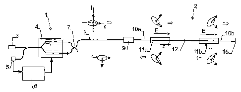
Fig. 1 shows a fiber-optic voltage sensor
having a control unit 1 and two sensing elements 2 using
a piezo-electrically induced birefringence change.
Control unit 1 comprises a light source 3, a
phase modulator 4 for a non-reciprocal phase modulation,
a light detector 5, a signal processor 6, and a polariza-
tion maintaining fiber coupler 7. Control unit 1 and the
sensing elements 2 form a polarization-rotated reflection
interferometer and use an interrogation technique as
known from fiber gyroscopes, for details see Ref. [5, 4].
Two orthogonal linearly polarized light waves
(indicated by solid and dashed arrows) exit from control
unit 1 and travel through a polarization maintaining (pm)
feed fiber 8 (e.g. an elliptical-core fiber) to a Faraday
CA 02672399 2009-06-11
WO 2008/077255 PCT/CH2006/000734
6
rotator 9 with a rotation angle of 45 per pass (or,
equivalently, a rotation angle of 45 + k=90 with k be-
ing any integer number). In other words, each light wave
is rotated by 45 each time it passes through Faraday ro-
tator 9. The rotation is non-reciprocal, i.e. the rota-
tion as seen from an observer looking towards the light
beam is, for example, clockwise if the beam propagates
from left to right, but counter-clockwise if the beam
propagates from right to left. The total rotation is thus
90 (or 90 + k=180 with k being an integer number). The
light waves exiting from Faraday rotator 9 are coupled
into a first pm sensing fiber 10a. The fast and slow axes
of this sensing fiber are oriented at 45 with regard to
the axes of the pm feed fiber 8 left of the rotator 9. As
a result the polarization directions after the rotation
again coincide with the birefingent fiber axes: A second
identical pm sensing fiber lOb is spliced at a splice 12
with its axes rotated by 90 with respect to first sens-
ing fiber 10a. The waves polarized parallel to slow axis
in first fiber 10a are then polarized along the fast axis
in second fiber lOb and vice versa. The waves are re-
flected at the end of second fiber 10b by a mirror 15 and
then retrace their paths. Non-reciprocal Faraday rotator
9 introduces another 45 rotation that adds to the first
rotation. The total rotation on the way forward and back-
ward is thus 90 ,-i.e. the light waves again return with
swapped polarizations to control unit 1, as in the cur-
rent sensor of EP 1 154 278. This is advantageous because
it keeps the total roundtrip path imbalance of the waves
3o at or near zero and thus within the coherence length of
the low coherent light source 3. Furthermore temperature
and vibration induced optical phase changes in the fiber
between modulator 4 and Faraday rotator 9 largely cancel
each other. Note: On a one way trip through the birefrin-
gent fibers 8, 1Oa, 10b the orthogonal waves accumulate a
path difference due to their different group velocities.
CA 02672399 2009-06-11
WO 2008/077255 PCT/CH2006/000734
7
Typically the path imbalance is 0.5 to 1 mm per meter of
fiber at a wavelength of 820 nm.
The two sensing fibers 10a, 10b to the right
of Faraday rotator 9 act as strain sensors and are used
to measure the periodic piezo-electric deformation of
piezoelectric quartz transducer elements 11a, 11b under
the influence of an alternating electric field (see be-
low). The induced fiber strain causes a differential
phase shift between the two orthogonal waves.
The two transducer elements 11a, 11b are ar-
ranged anti-parallel to each other, i.e. their polar axes
x (2-fold crystal axis of quartz) are anti-parallel as
shown in Fig. 1. The phase shifts in the sensing fibers
are then of the same sign if the electric field direc-
tions E are the same (as indicated).
The advantage of using a first and a second
sensing fiber 10a, 10b and transducer elements 11a, 11b
arranged opposite to each other are the following:
- The second pm sensing fiber lOb balances the optical
path imbalance between the two orthogonal waves in-
troduced in first sensing fiber 10a. Again this is
necessary to keep the total path imbalance within
the coherence length of a low coherent light source.
- Second sensing fiber 10b also compensates thermal
phase shifts in first fiber 10a provided the tem-
perature of the two fibers is about the same. Com-
pensation of large thermal phase shifts is necessary
as otherwise more sophisticated signal processing
might be needed. Ideally the total phase changes
should remain within an interval of n.
- Second fiber 10b allows to double the sensitivity of
the voltage sensor and to cancel vibration-induced
effects (see below).
The polarization-maintaining fibers are el-
liptical-core fibers, so-called Panda or bowtie fibers,
fibers with inner elliptical cladding, micro-structured
fibers or other types of pm fiber [8, 9].
CA 02672399 2009-06-11
WO 2008/077255 PCT/CH2006/000734
8
It should be noted that, with the detection
technique described here, the effective sensitivity of
the two pm sensing fibers 10a, 10b to alternating strain
varies as a function of the time delay between the for-
ward and backward propagating waves at the location of
the strain-applying transducer elements 11a, llb and thus
as a function of the length of the fibers. The strain-
induced phase shift is at its maximum if the time delay
is negligible compared to the period of the alternating
strain and becomes zero if the delay corresponds to half
a period of the strain. Furthermore, the effective sen-
sitivities of two sensing fibers 10a, lOb will differ if
the delay is not negligible. However, for the case con-
sidered below - a strain periodicity of 50 or 60 Hz and
fiber lengths up to some meters - the time delay is neg-
ligible and the delay effects can be disregarded.
Fig. 2 shows a modification of the set-up in
Fig. 1. A pm fiber coupler 13 and the two pm sensing fi-
bers 10a, 10b form a loop mirror. The coupler end at
Faraday rotator 9 is oriented like first sensing fiber
10a section in Fig. 1. The loop contains two 90 -splices
12, 14. The splices divide the loop in two halves with
identical lengths. An extra reflector is not needed. Two
pairs of orthogonal polarizations with orientations as
indicated counter-propagate in the loop. The functions
of the two loop halves are the same as the ones of the
two sensing fibers 10a, 10b in Fig. 1. The phase shifts
in the fibers 10a, 10b add if the crystallographic x-
directions and the field directions E are as indicated in
Fig. 2. A potential advantage of this configuration is
that for a symmetric arrangement of the transducer ele-
ments 11a, 11b the effective sensitivities are always the
same independent of the time delay (but the sensitivities
again decrease with increasing delay).
The phase modulator 4 in Figs. 1 and 2 is an
integrated-optics lithium modulator, see e.g. Ref. [4].
The modulator also acts as a polarizer. Another alterna-
CA 02672399 2009-06-11
WO 2008/077255 PCT/CH2006/000734
9
tive is a piezoelectric modulator as illustrated in Ref
[5].
Fig. 3 shows the same configuration as Fig. 1
but with a different type of integrated-optics phase
modulator 4. The modulator is a birefringence modulator
which directly modulates the phase of orthogonal light
waves. The pm coupler 7 of Fig. 2 is then no longer
needed. The depolarized light from light source 3 (depo-
larizer not shown) is polarized in a fiber polarizer 21
and subsequently coupled into an entrance pm fiber lead
22 of the modulator at splice 23. The polarization direc-
tion is at 45 to the axes of the pm fiber lead (45
splice). As a result two orthogonal waves of equal ampli-
tude are excited. The fast and slow axes of both pm fiber
leads 22, 8 of modulator 4 are parallel to the electro-
optic axes of the modulator.
Alternatively, a piezoelectric modulator as
illustrated in Ref. 6 may be used as a birefringence
modulator.
Fig. 4 shows an implementation of the inven-
tion based on a Sagnac type interferometer using two
Faraday rotators 8. There are two counter-propagating
waves having parallel polarizations between modulator 4
and the rotators 8 and orthogonal polarizations in the
first and second pm sensing fibers 10a, 10b with the
transducer elements 11a, 11b. The orientation of the fi-
ber cores at the rotators 8 is as above. The sensing fi-
bers are both rotated in the same direction, i.e. both
clockwise or both counter-clockwise, with regard to the
planes of polarization of the forward traveling waves be-
tween modulator 4 and the rotators B. The phase shifts in
the fibers 10a, 10b add if the crystallographic x-
directions and the field directions E are as indicated in
Fig. 4.
Figs. 5 and 6 show an arrangement of a piezo-
optic voltage sensor of the type of Figs. 1 - 4 for a
line integration of the electric field according to the
CA 02672399 2009-06-11
WO 2008/077255 PCT/CH2006/000734
present invention. Only the field sensing part of the
sensor is shown, i.e. the two pm sensing fibers 10a, 10b
and the transducer elements 11a, llb. The transducer
elements 11a, 11b are preferably identical quartz beams
5 (or platelets), according to Ref. 2. In the present em-
bodiment, two transducer elements are assigned to each
sensing fiber 10a, 10b. They may be arranged between
ground and high-voltage potentials with (equidistant),
non-negligible spacing between them or they can form an
10 essentially continuous quartz bridge as shown in Fig. 5.
In the latter case the beams may have a length of e.g.
200 mm and a cross-section of e.g. 2x2 mm2. The measure-
ment of e.g. 245 kV in high voltage substations may re-
quire 10-12 of such quartzes. The longitudinal axis of
the beams and the direction of the fiber coincide with a
crystallographic x-direction (2-fold crystal axis).
Quartz is a preferred material for the piezo-electric
transducers due to its superior material properties. Oth-
ers appropriate materials are given in Ref. 1, 2.
The two sensing fibers 10a, 10b are prefera-
bly attached to the transducer elements ila, 11b with the
90 -splice 12 at half the distance between ground and
high-voltage (Faraday rotator and mirror). The optical
phase shifts of the two fiber sections caused by the
thermal expansion of the quartzes are then the same and
cancel each other.
The x-directions (or polar directions) of the
quartzes of a given sensing fiber point in the same di-
rection. The x-directions along the second sensing fiber
10b are anti-parallel to the x-directions along the first
sensing fiber 10a. The sign of the optical phase shifts
at increasing or decreasing field strength is then the
same at all transducer elements as required for the line
integration of the field: The field-induced piezoelectric
strains at the two sensing fibers have oppo'site sign due
to the anti-parallel crystal directions; the two sensing
fibers react to a given change in strain also with oppo-
CA 02672399 2009-06-11
WO 2008/077255 PCT/CH2006/000734
11
site sign due to the 90 splice; as a result the combined
effects have the same sign. The overall phase shift is a
measure for the line integral of the field and thus the
voltage. A further benefit of the arrangement is that op-
tical phase shifts caused by external common-mode me-
chanical perturbations such as vibrations cancel each
other.
Preferably the sensing fibers 10a, 10b have a
coating which transmits, over a wide temperature range,
typically -40 to 85 C, the entire piezoelectric strain
from the quartzes to the sensing fibers (for example a
thin polyimide coating or coating of diamond like carbon
(DLC)). The sensing fibers are preferably attached to the
quartzes with some extensional pre-strain. The pre-strain
is sufficiently large so that sufficient strain is still
maintained when the quartzes contract at low tempera-
tures. The sensing fibers may be mounted to the quartz
surface or to a groove 16 in the surface with an appro-
priate bonding material. Alternatively, the fiber may be
attached in a through-hole along x.
The series of quartzes may be attached to a
common support structure 17 such as a strip of fiber re-
enforced epoxy. The strip may be mounted for mechanical
protection in a tube, cable or another enclosure (not
shown in Figs. 5, 6).
Figs. 7 and 8 show another arrangement
wherein the sensing elements 2 or sensing fibers 10a, 10b
are arranged side by side and optically coupled by a 90
splice 12 at neighboring ends 18a, 18b. The set-up com-
prises two parallel series of piezoelectric transducer
elements lla, 11b with axis directions x and a fiber ar-
rangement as indicated. The neighboring transducer ele-
ments 11a and 11b are mounted to a common support struc-
ture 17 as shown in Fig. 8. Advantages of this arrange-
ment are the following: (i) The sensitivity (optical
phase shift per voltage change) is doubled compared to
Fig. 5. (ii) Vibration-induced phase changes are can-
CA 02672399 2009-06-11
WO 2008/077255 PCT/CH2006/000734
12
celled more completely since the two quartz series are
very close to each other. Short wavelength vibrations are
still common-mode.
Further alternatives (not illustrated):
- Instead of two sensing fibers the sensor may contain
three or more sensing fibers spliced at 90 and hav-
ing lengths such that the total path imbalance of
the orthogonal light waves is again zero. The fibers
may be of the same or different type.
- The sensing fibers may be attached to a series of
transducer elements (or several series of transducer
elements) such that the fibers pass each series sev-
eral times, thus enhancing the sensitivity of the
sensor.
- The quartz beams or platelets may be replaced by
quartz cylinders with the sensing fibers attached to
the circumferential surface of the cylinders (see
Ref. 2).
- Only one sensing fiber may be attached to the trans-
ducer elements (quartzes) while the second section
only serves for compensation of the path imbalance.
Electro-optic voltage sensors:
Fig. 9 shows an electro-optic voltage sensor
according to the present invention. The first and second
sensing fibers 10a, 10b and the piezoelectric transducer
elements 11a, llb of Fig. 1 are replaced by an electro-
optic crystal 19. A collimator 20 between 45 Faraday ro-
tator 9 and crystal 19 generates a collimated beam which
is launched into crystal 19. The beam double passes crys-
tal 19 and is then coupled back into feed fiber 8. Due to
the 45 -rotator 9 the light waves again return with
swapped polarizations.
Preferably crystal 19 is suitable to line in-
tegration of the electric field. Appropriate crystal
classes and crystal orientations are listed in Tables 1
CA 02672399 2009-06-11
WO 2008/077255 PCT/CH2006/000734
13
and 2 of Ref. 10. The electro-optic axes of crystal 8 are
aligned at 45 with respect to the birefringent axes of
feed fiber 8. The polarization directions of the orthogo-
nal linearly polarized light waves in crystal 8 are then
parallel to the electro-optic axes. On their roundtrip
through crystal 19 the waves accumulate an electro-optic
phase shift proportional to the applied voltage. The
roundtrip phase shift is twice as large as the single
pass shift. Advantageously, the crystal belongs to one of
the classes of Table 1 in Ref. 10. These crystals are
free of any intrinsic birefringence. A preferred material
is Bi4(Ge04)3 (BGO).
In case of a birefringent crystal (Table 2)
it is advantageous to use a series of two identical crys-
tals 19a, 19b as shown in Fig. 10. The axes of birefrin-
gence (which are also the electro-optic axes) of the two
crystals 19a, 19b have a 90 -offset and the longitudinal
axes (a 2-fold axis for the materials of Table 2) are
anti-parallel. The phase shifts from the intrinsic bire-
fringence then cancel each other while the electro-optic
phase shifts add.
Instead of a bulk electro-optic crystal an
electro-optic crystal fiber may be used. The collimator
may be omitted in case of a crystalline single-mode fi-
ber.
The electro-optic crystal could also be part
of a loop mirror configuration according to Fig. 2 or a
Sagnac configuration according to Fig. 5.
Instead of using a 45 -Faraday rotator as
shown in the preceding embodiments, the polarization di-
rections of the returning light waves may be rotated by
means of two polarization-insensitive optical circulators
[11] as shown in Fig. 11. Fibers a and b are again po-
larization maintaining. The lengths of the various fiber
segments are such that the total path difference of the
two orthogonal waves is again zero. Fiber b (or fiber a)
may include a 90 -splice as indicated to rotate the po-
CA 02672399 2009-06-11
WO 2008/077255 PCT/CH2006/000734
14
larizations. Alternatively, the fibers may be attached to
the circulators with axes orientations such that polari-
zation directions of the returning waves are swapped as
desired.
The use of circulators instead of a simple
Faraday rotator offers no advantages and is mentioned
here only for the sake of completeness. Note that any
circulator contains at least one Faraday rotator.
1. REFERENCES
1. EP 316 635, EP 316 619
2. K. Bohnert and J. Nehring, Fiber-optic sensing of
voltages by line integration of the electric field,
Opt. Lett. 14, 290 (1989).
3. K. Bohnert, G. de Wit, and J. Nehring, Coherence-
tuned Interrogation of a remote elliptical-core,
dual-mode fiber strain sensor", K. Bohnert, G. de
Wit, and J. Nehring, J. of Lightwave Technology 13,
94 (1995) .
4."The fiber-optic gyroscope", Herve Lefevre, Artech
House, Boston, London, 1993.
5. EP 1 154 278
6. K. Bohnert, P.Gabus, J. Nehring, and H. Brandle,
"Temperature and vibration insensitive fiber-optic
current sensor", J. Lightw. Technol., vol: 20, no.
2, pp. 267-276, 2002.
7. K. Bohnert, P. Gabus, H. Brandle, Peter Guggenbach,
Fiber-optic dc current sensor for the electro-
winning industry", in 17th Int. Conference on Optical
Fibre Sensors, Bruges, Belgium, May 23-27, 2005, ed-
ited by M. Voet, R. Willsch, W. Ecke, J. Jones, B.
Culshaw, Proc. of SPIE Vol. 5855 (SPIE, Bellingham,
WA, 2005) 210-213.
8. J.Noda, K. Okamoto, and Y. Sasaki, "Polarization-
maintaining fibers and their applications", J.
Lightw. Technol. 4, 1071-1089, 1986.
CA 02672399 2009-06-11
WO 2008/077255 PCT/CH2006/000734
9. A. Orthigosa-Blanch et al., Highly birefringent
photonic crystal fibers, Optics Letters 25, 1325,
2000.
10. EP 682 261
5 11.Y.'Fujii, High-isolation polarization-independent
quasi-optical circulator, J. of Lightwave technology
10, 1226 (1992).
10 List of Reference Numerals
1: control unit
2: sensing element
3: light source
15 4: phase modulator
5: light detector
6: signal processor
7: pm fiber coupler
8: feed fiber
9: Faraday rotator
10a, 10b: sensing fibers
11a, llb: piezoelectric transducer elements
12: 90 splice
13: pm fiber coupler
14: 90 splice
15: mirror
16: groove
17: support
18: sensing fiber ends
19, 19a, 19b: electro-optic crystals
20: collimator
21: fiber polarizer
22: pm fiber lead
23: splice