Note: Descriptions are shown in the official language in which they were submitted.
CA 02673523 2009-06-19
WO 2008/083071 PCT/US2007/088548
METHOD OF GRINDING A SAPPHIRE SUBSTRATE
TECHNICAL FIELD
The present application is generally directed to sapphire substrates and
methods of finishing such
substrates.
BACKGROUND ART
Semiconducting components based on single crystal nitride materials of Group-
III and Group-V
elements are ideal for devices such as light-emitting diodes (LED), laser
diodes (LD), displays, transistors and
detectors, In particular, semiconductor elements utilizing Group-Ill and Group-
V nitride compounds are useful
for light emitting devices in the UV and blue/green wavelength regions. For
example, gallium nitride (GaN)
and related materials such as AlGaN, InGaN and combinations thereof, are the
most common examples of
nitride semiconductor materials in high demand.
However, manufacturing boules and substrates of such nitride semiconducting
materials has proven
difficult for a multitude of reasons. Accordingly, epitaxial growth of nitride
semiconducting materials on
foreign substrate materials is considered a viable alternative. Substrates
including SiC (silicon carbide), A1203
(sapphire or corundum), and MgAl2O4 (spinel) are common foreign substrate
materials.
Such foreign substrates have a different crystal lattice structure than
nitride semiconducting materials,
particularly GaN, and thus have a lattice mismatch. Despite such mismatch and
attendant problems such as
stresses and defectivity in the overlying semiconductor materials layer, the
industry demands large surface area,
high quality substrates, particularly sapphire substrates. However, challenges
remain with the production of
high quality substrates in larger sizes.
DISCLOSURE OF INVENTION
One embodiment is drawn to a sapphire substrate including a generally planar
surface having a
crystallographic orientation selected from the group consisting of a-plane, r-
plane, m-plane, and c-plane
orientation, and having a nTTV of not greater than about 0.037 m/cm2, wherein
nTTV is total thickness
variation normalized for surface area of the generally planar surface, the
substrate having a diameter not less
than about 9.0 cm.
Another embodiment is drawn to a sapphire substrate including a generally
planar surface having a
crystallographic orientation selected from the group consisting of a-plane, r-
plane, m-plane, and c-plane
orientation, and having a TTV of not greater than about 3.00 m, wherein TTV
is total thickness variation of the
generally planar surface. The substrate has a diameter not less than about 6.5
cm and a thickness not greater
than about 525 m.
-1-
CA 02673523 2009-06-19
WO 2008/083071 PCT/US2007/088548
Another embodiment is drawn to a method of machining a sapphire substrate
including grinding a first
surface of a sapphire substrate using a first fixed abrasive, and grinding the
first surface of the sapphire substrate
using a second fixed abrasive. The second fixed abrasive has a smaller average
grain size than the first fixed
abrasive, and the second fixed abrasive is self-dressing.
Another embodiment is drawn to a method of providing a sapphire substrate lot
containing sapphire
substrates that includes grinding a first surface of each sapphire substrate
using an abrasive such that the first
surface has a c-plane orientation, wherein the sapphire substrate lot contains
at least 20 sapphire substrates.
Each sapphire substrate has a first surface that has (i) a c-plane
orientation, (ii) a crystallographic m-plane
misorientation angle (Om), and (iii) a crystallographic a-plane misorientation
angle (0a), wherein at least one of
(a) a standard deviation am of misorientation angle Om is not greater than
about 0.0130 and (b) a standard
deviation 6a of misorientation angle Oa is not greater than about 0.0325.
Another embodiment is drawn to a sapphire substrate lot, including at least 20
sapphire substrates. Each
sapphire substrate has a first surface that has (i) a c-plane orientation,
(ii) a crystallographic m-plane
misorientation angle (Om), and (iii) a crystallographic a-plane misorientation
angle (Oa), wherein at least one of
(a) a standard deviation 6'm of misorientation angle Om is not greater than
about 0.0130 and (b) a standard
deviation na of misorientation angle 0a is not greater than about 0.0325.
BRIEF DESCRIPTION OF THE DRAWINGS
The present disclosure may be better understood, and its numerous features and
advantages made
apparent to those skilled in the art by referencing the accompanying drawings.
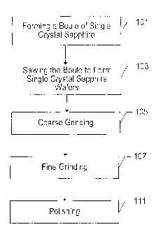
FIG. 1 is a flow chart illustrating a method of forming a substrate according
to one embodiment.
FIG. 2 is an illustration of a grinding apparatus according to one embodiment.
FIG. 3 is a plot comparing the use of a grinding tool according to one
embodiment as compared to a
traditional grinding tool.
FIG. 4 is an illustration of a polishing apparatus according to one
embodiment.
FIG. 5 is an illustration of misorientation angle of a c-plane oriented
sapphire substrate.
The use of the same reference symbols in different drawings indicates similar
or identical items.
DESCRIPTION OF THE EMBODIMENT(S)
According to an aspect, a method is provided that includes the steps of
grinding a first surface of a
sapphire substrate using a first fixed abrasive and grinding the first surface
of the sapphire substrate using a
second fixed abrasive. The method further provides that the second fixed
abrasive is finer than the first fixed
-2-
CA 02673523 2009-06-19
WO 2008/083071 PCT/US2007/088548
abrasive, such that the second fixed abrasive has a smaller average grain size
than the first fixed abrasive, and
the second fixed abrasive is a self-dressing abrasive surface.
By way of clarification, abrasives generally can be categorized as free
abrasives and fixed abrasives.
Free abrasives are generally composed of abrasive grains or grits in powder
form, or particulate form in a liquid
medium that forms a suspension. Fixed abrasives generally differ from free
abrasives in that fixed abrasives
utilize abrasive grits within a matrix of material which fixes the position of
the abrasive grits relative to each
other. Fixed abrasives generally include bonded abrasives and coated
abrasives. An example of a coated
abrasive is sandpaper; coated abrasives are typically planar sheets (or a
geometric manipulation of a planar
sheets to form a belt, flaps, or like), that rely on a flexible substrate on
which the grits and various size and make
coats are deposited. In contrast, bonded abrasives generally do not rely upon
such a substrate, and the abrasive
grits are fixed in position relative to each other by use of a matrix bond.
material in which the grits are
distributed. Such bonded abrasive components are generally shaped or molded,
and heat treated at a cure
temperature of the bond matrix (typically above 750 C) at which the bond
matrix softens, flows and wets the
grits, and cooled. Various three dimensional forms may be utilized, such as
annular, conical, cylindrical, frusto-
conical, various polygons, and may form as grinding wheels, grinding blocks,
grinding bits, etc. Particular
embodiments described herein utilize fixed abrasive components in the form of
bonded abrasives.
Referring to FIG. 1, a method of forming a substrate according to one
embodiment is illustrated by a
flow chart. The process is initiated by forming a boule of single crystal
sapphire at step 101. As will be
appreciated, the sapphire can be formed into a blank or a boule having any
size or shape suitable for use as a
substrate for semiconducting devices, particularly, LED/LD applications. As
such, a common shape is a boule
having a substantially cylindrical contour. The formation of single crystal
sapphire can be accomplished using
techniques such as the Czochralskij Method, Edge-Defined Film Fed Growth
(EFG), or Kyropoulos Method, or
other techniques depending upon the desired size and shape of the boule, and
the orientation of the crystal.
After forming the single crystal sapphire at step 101, sawing of the boule or
blank can be undertaken to
section the sapphire and form wafers at step 103. According to a particular
embodiment, sawing the sapphire
includes wire sawing a sapphire boule having a substantially cylindrical
shape. Wire sawing of the sapphire
boule provides a plurality of unfinished sapphire wafers. Generally, the
duration of the wire sawing process can
vary from about a few hours, such as about 2.0 hours to about 30 hours. The
desired thickness of the unfinished
sapphire wafers can be less than about 10 mm, such as less than about 8.0 mm
thick, or less than about 5.0 min
thick. According to one embodiment, the thickness of the sapphire wafers after
wire sawing at step 103, is less
than about 3.0 mm thick, such as less than about 1.0 mm thick.
According to one embodiment, wire sawing is carried out by using a fixed
abrasive wire element or
elements, such as an array of wires plated or coated with abrasive grains. In
one implementation, a
superabrasive, such as cubic boron nitride (CBN) or diamond is coated onto a
plurality of wires, and the
sapphire boule is rotated at high speeds (e.g., up to 5000 rpm) and pushed
against the wire grid, thereby slicing
the entire boule in a single step. One example of this technology is non-
spooling type wiresawing such as FAST
3-
CA 02673523 2009-06-19
WO 2008/083071 PCT/US2007/088548
(fixed abrasive slicing technology), offered by Crystal Systems Inc. of Salem,
Mass. Another example is spool-
to-spool wiresawing systems.
In the case of single crystal raw stock produced by the EFG process, typically
in the shape of a ribbon or
sheet, the wire sawing process may not be necessary, and cored-out (shaped)
wafers can proceed directly to a
grinding step.
For clarification, the terms "wafer" and "substrate" are used herein
synonymously to refer to sectioned
sapphire material that is being formed or processed, to be used as a substrate
for epitaxial growth of
semiconductor layers thereon, such as to form an optoelectronic device.
Oftentimes it is common to refer to an
unfinished sapphire piece as a wafer and a finished sapphire piece as a
substrate, however, as used herein, these
terms do not necessarily imply this distinction.
According to the embodiment illustrated in FIG. 1, after forming a plurality
of sapphire wafers via
sawing at step 103, the surfaces of the unfinished sapphire wafers can be
processed. Typically, one or both
major opposing surfaces of the unfinished sapphire wafers can undergo grinding
to improve the finish of the
surfaces. According to one embodiment, the unfinished sapphire wafers undergo
a coarse grinding process at
step 105. The coarse grinding step may include grinding both major surfaces of
the unfinished sapphire
substrates. Generally, the coarse grinding process removes a sufficient amount
of material to remove major
surface irregularities caused by the wire sawing process, at a reasonably high
material removal rate. As such,
the coarse grinding process may remove not less than about 30 microns of
material from a major surface of the
unfinished sapphire substrate, such as not less than about 40 microns, or not
less than about 50 microns of
material from a major surface of the unfinished sapphire wafers.
Generally, the coarse grinding process can utilize a fixed coarse abrasive
that includes coarse abrasive
grains in a bond material matrix. The coarse abrasive grains can include
conventional abrasive grains such as
crystalline materials or ceramic materials including alumina, silica, silicon
carbide, zirconia-alumina and the
like. In addition to or alternatively, the coarse abrasive grains can include
superabrasive grains, including
diamond, and cubic boron nitride, or mixtures thereof Particular embodiments
take advantage of superabrasive
grains. Those embodiments utilizing superabrasive grains can utilize non-
superabrasive ceramic materials such
as those noted above as a filler material.
In further reference to the coarse abrasive, the coarse abrasive grains can
have a mean particle size of not
greater than about 300 microns, such as not greater than about 200 microns, or
even not greater than about 100
microns. According to a particular embodiment, the mean particle size of the
coarse abrasive grains is within a
range of between about 2.0 microns and about 300 microns, such as within a
range of between about 10 microns
and 200 microns, and more particularly within a range of between about 10
microns and 100 microns. Typical
coarse grains have a mean particle size within a range of about 25 microns to
75 microns.
As described above, the coarse abrasive includes a bond material matrix.
Generally, the bond material
matrix can include a metal or metal alloy. Suitable metals include iron,
aluminum, titanium, bronze, nickel,
silver, zirconium, alloys thereof and the like. In one embodiment, the coarse
abrasive includes not greater than
-.4-
CA 02673523 2012-01-10
about 90 vol% bond material, such as not greater than about 85 vol% bond
material. Typically, the coarse
abrasive includes not less than about 30 vol% bond material, or even not less
than about 40 vol% bond material.
In a particular embodiment, the coarse abrasive includes an amount of bond
material within a range of between
about 40 vol% and 90 vol%. Examples of particular abrasive wheels include
those described in US 6,102,789;
US 6,093,092; and US 6,019,668.
Generally, the coarse grinding process includes providing an unfinished
sapphire wafer on a holder and
rotating the sapphire wafer relative to a coarse abrasive surface. Referring
briefly to FIG. 2, a diagram of a
typical grinding apparatus 200 is illustrated, shown in partial cut-away
schematic form. The grinding apparatus
200 can include an unfinished wafer 203 provided on a holder 201, such that
the wafer 203 is at least partially
recessed into the holder 201. The holder 201 can be rotated, thus rotating the
unfinished wafer 203. A grinding
wheel 205 (shown in cut-away form) having an abrasive rim 207, can be rotated
relative to the unfinished wafer
203 thus grinding the surface of the unfinished wafer; the wafer 203 and the
grinding wheel 205 may be rotated
about the same direction (e.g., both clockwise or counter-clockwise), while
grinding is effected due to the offset
rotational axes. As illustrated, in addition to rotating the grinding wheel
205, a downward force 209 can be
applied to the grinding wheel 203.
As illustrated, the coarse abrasive can be an abrasive wheel having a
substantially circular abrasive rim
207 around a perimeter of an inner wheel. According to one embodiment, the
fine grinding process includes
rotating the abrasive wheel at a speed of greater than about 2000 revolutions
per minute (rpm), such as greater
than about 3000 rpm, such as within a range of 3000 to 6000 rpm. Typically, a
liquid coolant is used, including
aqueous and organic coolants.
In a particular embodiment, a self-dressing coarse abrasive surface is
utilized. Unlike many
conventional fixed abrasives, a self-dressing abrasive generally does not
require dressing or additional
conditioning during use, and is particularly suitable for precise, consistent
grinding. In connection with self-
dressing, the bond material matrix may have particular composition, porosity,
and concentration relative to the
grains, to achieve desired fracture of the bond material matrix as the
abrasive grains develop wear flats. Here,
the bond material matrix fractures as wear flats develop due to increase in
loading force of the matrix. Fracture
desirably causes loss of the worn grains, and exposes fresh grains and fresh
cutting edges associated therewith.
In particular, the bond material matrix of the self-dressing coarse abrasive
can have a fracture toughness less
than about 6.0 MPa-m112, such as less than about 5.0 MPa-m"2, or particularly
within a range of between about
1.0 MPa-m1'2 and 3.0 MPa-m112.
Generally, a self-dressing coarse abrasive partially replaces the bond
material with pores, typically
interconnected porosity. Accordingly, the actual content of the bond material
is reduced over the values noted
above. In one particular embodiment, the coarse abrasive has a porosity not
less than about 20 vol%, such as
not less than about 30 vol%, with typical ranges between about 30 vol% and
about 80 vol%, such as about 30
vol% to about 80 vol% and about 30 vol% to about 70 vol%. According to one
embodiment, the coarse
abrasive includes about 50 vol% to about 70 vol% porosity. It will be
appreciated that, the porosity can be open
or closed, and in coarse abrasives that have a greater percentage of porosity,
generally the porosity is open,
-5-
CA 02673523 2009-06-19
WO 2008/083071 PCT/US2007/088548
interconnected pores. The size of the pores can generally be within a range of
sizes between about 25 microns
to about 500 microns, such as between about 150 microns to about 500 microns.
The foregoing pore-related
values and those described herein are made in connection with various
components pre-machining or pre-
grinding.
According to one embodiment, the coarse abrasive grain content is confined in
order to further improve
self-dressing capabilities. For example, the coarse abrasive contains not
greater than about 50 vol%, not greater
than 40 vol%, not greater than 30 vol%, such as not greater than about 20
vol%, or even not greater than about
vol% coarse abrasive grains. In one particular embodiment, the coarse abrasive
includes not less than about
0.5 vol% and not greater than about 25 vol% coarse abrasive grains, such as
within a range of between about 1.0
10 vol% and about 15 vol% coarse abrasive grains, or particularly within a
range of between about 2.0 vol% and
about 10 vol% coarse abrasive grains.
Referring briefly to FIG. 3, two plots are illustrated that compare the normal
force applied to the
grinding wheel as a function of grinding time between a self-dressing abrasive
surface and a traditional abrasive
surface. As illustrated, the self-dressing abrasive has a substantially
constant peak normal force during each of
the three illustrated grinding operations 301, 302, and 303 (301-303). In
addition, the peak normal force is not
substantially different between each of the grinding operations 301-303. In
contrast, the traditional abrasive
surface illustrates an increase in the force necessary to effectively grind a
surface between individual grinding
operations 304, 305, 306, and 307 (304-307) as well as during each of the
individual grinding operations 304-
307. Such normal force increases during grinding is more likely to cause
notable surface and subsurface defects
(high defect density) and inconsistent grinding, even with frequent dressing
operations.
According to one embodiment, the peak normal force during grinding using the
self-dressing coarse
abrasive includes applying a force normal to the substrate surface of not
greater than about 200 N/mm width (as
measured along the contact area between the substrate and grinding wheel) for
the duration of the grinding
operation. In another embodiment, the peak normal force applied is not greater
than about 150 N/mm width,
such as not greater than about 100 N/mm width, or even not greater than about
50 N/mm width for the duration
of the grinding operation.
After coarse grinding, the wafers typically have an average surface roughness
Ro of less than about 1
micron. Typically, fine grinding is then carried out not only to improve
macroscopic features of the substrate,
including flatness, bow, warp, total thickness variation., and surface
roughness, but also finer scale defects such
as reduction in subsurface damage such as damaged crystallinity, including
particularly reduction or removal of
crystalline dislocations.
In some circumstances, the first coarse grinding step may be omitted or
replaced by lapping, which
utilizes a free abrasive typically in the form of a slurry. In such a case,
the second grinding operation utilizes the
self-dressing fixed abrasive noted above.
Turning back to the embodiment illustrated in FIG. 1, upon completion of
coarse grinding at step 105,
the sapphire wafers can be subject to a fine grinding process at step 107. The
fine grinding process generally
-6-
CA 02673523 2009-06-19
WO 2008/083071 PCT/US2007/088548
removes material to substantially remove defects caused by the coarse grinding
process 105. As such, according
to one embodiment, the fine grinding process removes not less than about 5.0
microns of material from a major
surface of the sapphire substrate, such as not less than about 8.0 microns,
or, not less than about 10 microns of
material from a major surface of the sapphire wafers. In another embodiment,
more material is removed such
that not less than about 12 microns, or even not less than about 15 microns of
material is removed from a
surface of the sapphire substrate. Typically, fine grinding at step 107 is
undertaken on one surface, as opposed
to the coarse grinding process at step 105 which can include grinding both
major surfaces of the unfinished
sapphire wafers.
The fine abrasive can utilize a fixed fine abrasive that includes fine
abrasive grains in a bond material
matrix. The fine abrasive grains can include conventional abrasive grains such
as crystalline materials or
ceramic materials including alumina, silica, silicon carbide, zirconia-alumina
or superabrasive grains such as
diamond and cubic boron nitride, or mixtures thereof. Particular embodiments
take advantage of superabrasive
grains. Those embodiments utilizing superabrasive grains can utilize non-
superabrasive ceramic materials such
as those noted above as a filler material.
According to one embodiment, the fine abrasive contains not greater than about
50 vol%, not greater
than 40 vol%, not greater than 30 vol%, such as not greater than about 20
vol%, or even not greater than about
10 vol% fine abrasive grains. In one particular embodiment, the fine abrasive
includes not less than about 0.5
vol% and not greater than about 25 vol% fine abrasive grains, such as within a
range of between about 1.0 vol%
and about 15 vol% fine abrasive grains, or particularly within a range of
between about 2.0 vol% and about 10
vol% fine abrasive grains.
In further reference to the fine abrasive, the fine abrasive grains can have a
mean particle size of not
greater than about 100 microns, such as not greater than about 75 microns, or
even not greater than about 50
microns. According to a particular embodiment, the mean particle size of the
fine abrasive grains is within a
range of between about 2.0 microns and about 50 microns, such as within a
range of between about 5 microns
and about 35 microns. Generally, the difference in mean particle sizes between
the coarse and fine fixed
abrasives is at least 10 microns, typically at least 20 microns.
Like the coarse abrasive, the fine abrasive includes a bond material matrix
that can include materials
such as a metal or metal alloy. Suitable metals can include iron, aluminum,
titanium, bronze, nickel, silver,
zirconium, and alloys thereof. In one embodiment, the fine abrasive includes
not greater than about 70 vol%
bond material, such as not greater than about 60 vol% bond material, or still
not greater than about 50 vol%
bond material. According to another embodiment, the fine abrasive includes not
greater than about 40 vo1%
bond material. Generally, the fine abrasive includes an amount of bond
material not less than about 10 vol%,
typically not less than 15 vol%, or not less than 20 vol%.
Further, the fine fixed abrasive may include a degree of porosity. In one
particular embodiment, the fine
abrasive has a porosity not less than about 20 vol%, such as not less than
about 30 vol%, with typical ranges
between about 30 vol% and about 80 vol%, such as about 50 vol% to about 80
vol% or about 30 vol% to about
70 vol%. According to one embodiment, the fine abrasive includes about 50 vol%
to 70 vol% porosity. It will
-7-
CA 02673523 2012-01-10
be appreciated that, the porosity can be open or closed, and in fine abrasives
that have a greater percentage of
porosity, generally the porosity is open, interconnected pores. The size of
the pores can generally be within a
range of sizes between about 25 microns to about 500 microns, such as between
about 150 microns to about 500
microns.
In reference to the fine grinding process at step 107, as mentioned
previously, the fine abrasive is self-
dressing. Similar to the self-dressing coarse abrasive, the self-dressing fine
abrasive includes a bond material
matrix, which typically includes a metal having a particular fracture
toughness. According to one embodiment,
the bond material matrix can have a fracture toughness less than about 6.0 MPa-
m112, such as less than about 5.0
MPa-m'12, or particularly within a range of between about 1.0 MPa-m'12 and
about 3.0 MPa-m112. Self-dressing
fine grinding components are described in US 6,755,729 and US 6,685,755.
Generally, the fine grinding process 107 includes an apparatus and process
similar to the process
described above in conjunction with the coarse grinding process 105. That is,
generally, providing an
unfinished sapphire wafer on a holder and rotating the sapphire wafer relative
to a fine abrasive surface,
typically an abrasive wheel, having a substantially circular abrasive rim
around a perimeter of an inner wheel.
According to one embodiment, the fine grinding process includes rotating the
abrasive wheel at a speed of
greater than about 2000 revolutions per minute (rpm), such as greater than
about 3000 rpm, such as within a
range of 3000 to 6000 rpm. Typically, a liquid coolant is used, including
aqueous and organic coolants.
As stated above, the fine abrasive can be self-dressing and as such generally
has characteristics discussed
above in accordance with the self-dressing coarse abrasive. However, according
to one embodiment, the peak
normal force during fine grinding includes applying a force of not greater
than about 100 N/mm width for the
duration of the grinding operation. In another embodiment, the peak normal
force is not greater than about 75
N/mm width, such as not greater than about 50 N/mm width, or even not greater
than about 40 N/mm width for
the duration of the grinding operation.
The description of coarse and fine abrasives above refers to the fixed
abrasive components of the actual
grinding tool. As should be clear, the components may not form the entire body
of the tool, but only the portion
of the tool that is designed to contact the workpiece (substrate), and the
fixed abrasive components may be in
the form of segments.
After fine grinding of the unfinished sapphire wafers the wafers typically
have an average surface
roughness Ra of less than about 0.10 microns, such as less than about 0.05
microns.
After fine grinding the sapphire wafers 107, the wafers can be subjected to a
stress relief process such as
those disclosed in EP 0 221 454 B 1. As described, stress relief may be
carried out by an etching or annealing
process. Annealing can be carried out at a temperature above 1000 C for
several hours.
Referring again to the embodiment of FIG. 1, after fine grinding at step 107,
the ground sapphire wafer
can be subjected to polishing at step 111. Generally, polishing utilizes a
slurry that is provided between the
-8-
CA 02673523 2009-06-19
WO 2008/083071 PCT/US2007/088548
surface of the wafer and a machine tool, and the wafer and the machine tool
can be moved relative to each other
to carry out the polishing operation. Polishing using a slurry generally falls
into the category of chemical-
mechanical polishing (CMP) and the slurry can include loose abrasive particles
suspended in a liquid medium to
facilitate removal of a precise amount of material from the wafer. As such,
according to one embodiment, the
polishing process 111 can include CMP using a slurry containing an abrasive
and an additive compound, which
may function to enhance or moderate material removal. The chemical component
may, for example, be a
phosphorus compound. Effectively, the abrasive provides the mechanical
component, and the additive provides
the chemically active component.
The loose abrasive is generally nanosized, and has an average particle
diameter less than 1 micron,
typically less than 200 nanometers. Typically, the median particle size is
within a slightly narrower range, such
as within a range of about 10 to about 150 nm. For clarification of technical
terms, a median particle size of
under about 1 micron generally denotes a polishing process, corresponding to
the subject matter hereinbelow, in
which a fine surface finish is provided by carrying out the machining
operation at low material removal rates.
At median particle sizes above about 1.0 micron, such as on the order of about
2.0 to about 5.0 microns,
typically the machining operation is characterized as a lapping operation. A
particularly useful loose abrasive is
alumina, such as in the form of polycrystalline or monocrystalline gamma
alumina.
As discussed above, a phosphorus additive may be present in the slurry.
Typically, the phosphorus
additive is present at a concentration within a range of between about 0.05 to
about 5.0 wt%, such as within a
range of between about 0.10 wt% to about 3.0 wt%. Particular embodiments
utilize a concentration within a
slightly narrower range, such as on the order of about 0.10 wt% to about 2.0
wt%. According to one
embodiment, the phosphorus compound contains oxygen, wherein oxygen is bonded
to the phosphorus element.
This class of materials is known asoxophosphorus materials. Particularly, the
oxophosphorus compound
contains phosphorus in valency state of one, three or five, and in particular
embodiments, effective machining
has been carried out by utilizing anoxophosphorus compound in which the
phosphorus is in a valency state of
five.
In other embodiments, the phosphorus can be bonded to carbon in addition to
oxygen, which generally
denotes organic phosphorus compounds known as phosphonates. Other phosphorus
compounds include
phosphates, pyrophosphates, hypophosphates, subphosphates, phosphites,
pyrophosphites, hypophosphites and
phosphonium compounds. Particular species of phosphorus compounds include
potassium phosphate, sodium
hexametaphosphate, hydroxy phosphono acetic acid (Belcor 575) and aminotri-
(methylenephosphonicacid)
(Mayoquest 1320).
Generally the slurry containing the abrasive component and the additive
containing the phosphorus
compound is aqueous, that is, water-based. In fact the slurry generally has a
basic pH, such that the pH is
greater than about 8.0, such as greater than about 8.5. The pH may range up to
a value of about twelve.
Referring briefly to the apparatus for polishing the ground sapphire wafer,
FIG. 4 illustrates a schematic
of the basic structure of a polishing apparatus according to one embodiment.
The apparatus 401 includes a
machine tool, which in this case is formed by a polishing pad 410 and a
platen, which supports the polishing
-9-
CA 02673523 2009-06-19
WO 2008/083071 PCT/US2007/088548
pad. The platen and polishing pad 410 are of essentially the same diameter.
The platen is rotatable about a
central axis, along a direction of rotation as illustrated by the arrow. A
template 412 has a plurality of circular
indentations which respectively receive substrates 414, the substrates 414
being sandwiched between the
polishing pad 410 and the template 412. The template 412, carrying the
substrates 414, rotates about its central
axis, wherein rp represents the radius from the center of rotation of the
polishing pad to the center of the
template 412, whereas rt represents the radius from an individual substrate to
the center of rotation of the
template. The configuration of apparatus 401 is a commonly employed
configuration for polishing operations,
although different configurations may be utilized.
The addition of a phosphorous compound to the slurry generally improves the
material removal rate
(MRR) over slurries having no phosphorus-based additive. In this regard, the
improvement can be indicated by
a ratio MRRadd/MRRc0,,,, which according to one embodiment, is not less than
about 1.2. The designation
MRRadd is the material removal rate of a slurry comprising an abrasive and the
additive containing the
phosphorus compound, whereas MRRCOõ is the material removal rate under
identical process conditions with a
control slurry, the control slurry being essentially identical to the above-
mentioned slurry but being free of the
additive containing the phosphorus compound. According to other embodiments,
the ratio was greater, such as
not less than about 1.5, or even not less than about 1.8, and in some certain
samples twice the removal rate over
a slurry containing only an alumina abrasive and no phosphorus compound
additive.
While the foregoing has focused on various embodiments, including embodiments
based on alumina-
based polishing slurries, other abrasive materials may be used as well with
excellent results, including silica,
zirconia, silicon carbide, boron carbide, diamond, and others. Indeed, the
zirconia based slurries containing a
phosphorus-based compound have demonstrated particularly good polishing
characteristics, namely 30-50%
improved material removal rates over silica alone on alumina substrates.
According to particular aspect, a high surface area sapphire substrate is
provided that includes a
generally planar surface having an a-plane orientation, an r-plane
orientation, an m-plane orientation, or a c-
plane orientation, and which includes controlled dimensionality. As used
herein, "x-plane orientation" denotes
the substrates having major surfaces that extend generally along the
crystallographic x-plane, typically with
slight misorientation from the x-plane according to particular substrate
specifications, such as those dictated by
the end-customer. Particular orientations include the r-plane and c-plane
orientations, and certain embodiments
utilize a c-plane orientation.
As noted above, the substrate may have a desirably controlled dimensionality.
One measure of
controlled dimensionality is total thickness variation, including at least one
of TTV (total thickness variation)
and nTTV (normalized total thickness variation).
For example, according to one embodiment, the TTV is generally not greater
than about 3.00 m, such
as not greater than about 2.85 m, or even not greater than about 2.75 m. The
foregoing TTV parameters are
associated with large-sized wafers, and particularly large-sized wafers having
controlled thickness. For
example, embodiments may have a diameter not less than about 6.5 cm, and a
thickness not greater than about
490 m. According to certain embodiments, the foregoing TTV parameters are
associated with notably larger
-10-
CA 02673523 2009-06-19
WO 2008/083071 PCT/US2007/088548
sized wafers, including those having diameters not less than 7.5 cm, not less
than 9.0 cm, not less than 9.5 cm,
or not less than 10.0cm. Wafer size may also be specified in terms of surface
area, and the foregoing TTV
values may be associated with substrates having a surface area not less than
about 40 cm2, not less than about 70
cm2, not less than about 80 cm2, or even not less than about 115 cm2. In
addition, the thickness of the wafers
may be further controlled to values not greater than about 500 m, such as not
greater than about 490 gm.
It is noted that the term `diameter' as used in connection with wafer,
substrate, or boule size denotes the
smallest circle within which the wafer, substrate, or boule fits. Accordingly,
to the extent that such components
have a flat or plurality of flats, such flats do not affect the diameter of
the component.
Various embodiments have well controlled nTTV, such as not greater than about
0.037 m/cm2.
Particular embodiments have even superior nTTV, such as not greater than 0.035
m/cm2, or even not greater
than 0.032 m/cm2. Such controlled nTTV has been particularly achieved with
large substrates, such as those
having a diameter not less than about 9.0 cm, or even not less than about 10.0
cm. Wafer size may also be
specified in terms of surface area, and the foregoing nTTV values may be
associated with substrates having a
surface area not less than about 90 cm2, not less than about 100 cm2, not less
than about 115 cm3.
Referring to the total thickness variation values of the sapphire substrate,
TTV is the absolute difference
between the largest thickness and smallest thickness of the sapphire substrate
(omitting an edge exclusion zone
which typically includes a 3.0 mm ring extending from the wafer edge around
the circumference of the wafer),
and nTTV is that value (TTV) normalized to the surface area of the sapphire
substrate. A method for measuring
total thickness variation is given inASTM standard F1530-02.
Generally, the nTTV value, as well as all other normalized characteristics
disclosed herein, are
normalized for a sapphire substrate having a generally planar surface and
substantially circular perimeter which
can include a flat for identifying the orientation of the substrate. According
to one embodiment, the sapphire
substrate has a surface area of not less than about 25 cm 2, such as not less
than about 30 cm2, not less than 35
cm2 or even not less than about 40 cm'. Still, the substrate can have a
greater surface area such that the
generally planar surface has a surface area not less than about 50 cm2, or
still not less than about 60 cm2, or not
less than about 70 cm2 The sapphire substrates may have a diameter greater
than about 5.0 cm (2.0 inches),
such as not less than about 6.0 cm (2.5 inches). However, generally the
sapphire substrates have a diameter of
7.5 cm ( 3.0 inches) or greater, specifically including 10 cm (4.0 inches)
wafers.
In further reference to characteristics of the sapphire substrate, according
to one embodiment, the
generally planar surface of the sapphire substrate has a surface roughness Ra
of not greater than about 100.0 A,
such as not greater than about 75.0 A, or about 50.0 A, or even not greater
than about 30.0 A. Even superior
surface roughness can be achieved, such as not greater than about 20.0 A, such
as not greater than about 10.0 A,
or not greater than about 5.0 A.
The generally planar surface of the sapphire substrate processed in accordance
with the methods
described above can have superior flatness as well. The flatness of a surface
is typically understood to be the
maximum deviation of a surface from a best-fit reference plane (see ASTM F
1530-02). In this regard,
-11-
CA 02673523 2009-06-19
WO 2008/083071 PCT/US2007/088548
normalized flatness is a measure of the flatness of the surface normalized by
the surface area on the generally
planar surface. According to one embodiment, the normalized flatness
(nFlatness) of the generally planar
surface is greater than about 0.100 m/cm2, such as not greater than about
0.080 m/cm2, or even not greater
than about 0.070 m/cm2. Still, the normalized flatness of the generally
planar surface can be less, such as not
greater than about 0.060 m/cm2, or not greater than about 0.050 m/cm2.
Sapphire substrates processed in accordance with methods provided herein can
exhibit a reduced
warping as characterized by normalized warp, hereinafter nWarp. The warp of a
substrate is generally
understood to be the deviation of the median surface of the substrate from a
best-fit reference plane (see ASTM
F 697-92(99). In regards to the nWarp measurement, the warp is normalized to
account for the surface area of
the sapphire substrate. According to one embodiment, the nWarp is not greater
than about 0.190 m/cm2, such
as not greater than about 0.170 m/cm2, or even not greater than about 0.150
m/cm2.
The generally planar surface can also exhibit reduced bow. As is typically
understood, the bow of a
surface is the absolute value measure of the concavity or deformation of the
surface, or a portion of the surface,
as measured from the substrate centerline independent of any thickness
variation present. The generally planar
surface of substrates processed according to methods provided herein exhibit a
reduced normalized bow (nBow)
which is a bow measurement normalized to account for the surface area of the
generally planar surface. As
such, in one embodiment the nBow of the generally planar surface is not
greater than about 0.100 m/cm2, such
as not greater than about 0.080 m/cm2, or even not greater than about 0.070
m/cm2. According to another
embodiment, the nBow of the substrate is within a range of between about 0.030
gm/cm2 and about 0.100
m/cm2, and particularly within a range of between about 0.040 m/cm2 and about
0.090 m/cm2.
In reference to the orientation of the sapphire substrate, as described above,
the generally planar surface
has a c-plane orientation. C-plane orientation can include a manufactured or
intentional tilt angle of the
generally planar surface from the c-plane in a variety of directions. In this
regard, according to one
embodiment, the generally planar surface of the sapphire substrate can have a
tilt angle of not greater than about
2.0 , such as not greater than about 1.0 . Typically, the tilt angle is not
less than about 0.10 , or not less than
0.15 . Tilt angle is the angle formed between the normal to the surface of the
substrate and the c-plane.
According to embodiments herein, processing of sapphire wafers desirably
results in well controlled
wafer-to-wafer precision. More specifically, with respect to c-plane oriented
wafers the precise orientation of
the wafer surface relative to the c-plane of the sapphire crystal is fixed
precisely, particularly as quantified by
wafer-to-wafer crystallographic variance. With reference to FIG. 5, Z is a
unit normal to the polished surface of
the sapphire, and 0A , OM and Oc are orthonormal vectors normal to an a-plane,
an m-plane and a c-plane
respectively. A and M are projections of OA , OM respectively on the plane
defined by the sapphire surface (A =
OA - Z ( OA Z) , M = 0M - Z (OM .Z)). The misorientation angle in the a-
direction is the angle between OA and its
projection on the plane containing A and M, and the misorientation angle in
the in-direction is the angle between
OM and its projection on the plane containing A and M. Misorientation angle
standard deviation a is the standard
deviation of misorientation angle across a wafer lot, typically at least 20
wafers.
-12-
CA 02673523 2009-06-19
WO 2008/083071 PCT/US2007/088548
According to embodiments, processing is carried out as described herein,
particularly incorporating the
grinding process described in detail above, and a lot of sapphire wafers are
provided that has precise
crystallographic orientation. Substrate lots typically have not fewer than 20
wafers, oftentimes 30 or more
wafers, and each lot may have wafers from different sapphire cores or boules.
It is noted that a lot may be
several sub-lots packaged in separate containers. The wafer lots may have a
standard deviation 6M of OM across
a wafer lot not greater than about 0.0130 degrees, such as not greater than
0.0110 degrees, or not greater than
0.0080 degrees. The wafer lots may have a standard deviation 6A of OA not
greater than about 0.0325 degrees,
such as not greater than 0.0310 degrees, or not greater than 0.0280 degrees.
In comparison with prior methods of manufacturing wafers/substrates for LED/LD
substrates, present
embodiments provide notable advantages. For example, according to several
embodiments, utilization of a
coarse grinding abrasive (oftentimes a self-dressing coarse fixed abrasive) in
conjunction with a self-dressing
fine grinding abrasive, as well as particular CMP polishing techniques and
chemistries, facilitate production of
precision finished sapphire wafers having superior geometric qualities (i.e.,
nTTV, nWarp, nBow, and
nFlatness). In addition to the control of geometric qualities, the processes
provided above in conjunction with
precision wire sawing facilitates precision oriented crystal wafers having
superior control of the tilt angle
variation across substrates. In these respects, the improved geometric
qualities and precise control of surface
orientation from substrate to substrate, facilitates production of consistent
LED/LD devices having more
uniform light emitting qualities.
Following the various processing steps described herein, the surface of the
sapphire substrate subjected
to treatment generally has a suitable crystal structure for use in LED/LD
devices. For example, embodiments
have a dislocation density less than1E6/cm2 as measured by X-ray topographic
analysis.
It is particularly noteworthy that dimensional and/or crystallographic
orientation control is achieved by
embodiments of the invention in connection with large sized substrates and
substrates having controlled
thickness. In these respect, according to the state of the art, dimensional
and crystallographic controls degrade
rapidly with increase in wafer size (surface area) for a given thickness.
Accordingly, state of the art processing
has typically relied on increasing thickness in an attempt to at least
partially maintain dimensional and
crystallographic control. In contrast, embodiments herein can provide such
controls largely independent of
thickness and less dependent on wafer or substrate size.
EXAMPLES
The following examples provide methods for processing wafers according to
several embodiments, and
particularly describe processing parameters for production of high surface
area wafers having improved
dimensional qualities and orientations. In the following examples, c-plane
sapphire wafers having diameters of
2 inches, 3 inches, and 4 inches were processed and formed in accordance with
embodiments provided herein.
Processing initiates with a boule that is sectioned or sliced, as described
above. The boule is sectioned
using a wire sawing technique, wherein the boule is placed and rotated over
wires coated with cutting elements,
such as diamond particles. The boule is rotated at a high rate of speed,
within a range of between about 2000
-13-
CA 02673523 2009-06-19
WO 2008/083071 PCT/US2007/088548
rpm and 5000 rpm. While the boule is rotating it is in contact with multiple
lengths of wiresaw, which are
typically reciprocated at a high speed in a direction tangential to the
surface of the boule, to facilitate slicing.
The lengths of wiresaw are reciprocated at a speed of about 100 cycles/minute.
Other liquids can be
incorporated, such as a slurry to facilitate slicing. In this instance, the
wire sawing process lasts a few hours,
within a range of between about 4 to 8 hours. It will be appreciated that the
duration of the wire sawing process
is at least partially dependent upon the diameter of the boule being sectioned
and thus may last longer than 8
hours.
After wire sawing, the wafers have an average thickness of about 1.0 mm or
less. Generally, the wafers
have an average surface roughness (Ra) of less than about 1.0 micron, an
average total thickness variation of
about 30 microns, and an average bow of about 30 microns.
After wire sawing the boule to produce wafers, the wafers are subjected to a
grinding process. The
grinding process includes at least a first coarse grinding process and a
second fine grinding process. In regards
to the coarse grinding process, a self-dressing coarse grinding wheel is used,
such as a PICO type wheel, Coarse
#3-17-XL040, manufactured by Saint-Gobain Abrasives, Inc., which incorporates
diamond grit having an
average grit size within a range of about 60 to 80 microns. For this example,
coarse grinding of the wafers is
completed using a Strasbaugh 7AF ultra precision grinder. The cycles and
parameters of the coarse grinding
process are provided in Table 1 below.
In the Tables 1 and 2 below, material is successively removed through a series
of iterative grinding steps.
Steps 1-3 represent active grinding steps at the indicated wheel and chuck
speeds and feed rate. Dwell is carried
out with no bias, that is, a feed rate of zero. Further, lift is carried out
at a feed rate in the opposite direction, the
wheel being lifted from the surface of the substrate at the indicated feed
rate.
Table 1:
Wheel speed=2223 rpm Step 1 Step 2 Step 3 Dwell Lift
Material removed (um) 40 5 5 25 rev 10
Feed rate (um/s) 3 1 1 1
Chuck speed (rpm) 105 105 105 105 105
After the coarse grinding process, the wafers are subject to a fine grinding
process. The fine grinding
process also utilizes a self-dressing wheel, such as an IRIS type wheel Fine
#4-24-XL073, manufactured by
Saint-Gobain Abrasives, Inc., which utilizes diamond abrasive grit having an
average grit size within a range of
about 10-25 microns. Again, for the purposes of this example, the fine
grinding of the wafers is completed
using a Strasbaugh 7AF ultra precision grinder. As with the coarse grinding
process, the fine grinding process
subject the wafers to particular processing cycles and parameters which are
provided in Table 2 below.
-14-
CA 02673523 2009-06-19
WO 2008/083071 PCT/US2007/088548
Table 2
Wheel speed=2633 rpm Step 1 Step 2 Step 3 Dwell Lift
Material removed (um) 10 3 2 55 rev 5
Feed rate (um/s) 1 0.1 0.1 0.5
Chuck speed (rpm) 55 55 55 55 55
After the coarse and fine grinding processes, the sapphire wafers are
subjected to a stress relief process
as described above.
After stress relief, the sapphire wafers are subjected to a final polishing.
Several polishing slurries were
prepared to investigate the role of pH and phosphates as well as the role of
alkali and calcium. Reported below,
Table 3 shows enhancements to a baseline slurry, Slurry 1. Polishing was
carried out utilizing C-plane sapphire
pucks, 2" in diameter, polished on a Buehler ECOMET 4 polisher. Polishing was
done on a H2 pad (available
from Rohm and Haas Company of Philadelphia, PA) with a slurry flow rate of 40
ml/min at a platen speed of
400 rpm, carrier speed of 200 rpm at a downforce of 3.8psi.
Table 3
Slurry H MRR Starting Ra Ra at 60 min - Ra at 60 minutes - Ra at 60 minutes -
Number p (A/min) (A) Center (A) Middle (A) Edge (A)
1 9 842 7826 443 100 26
2 10 800 7686 481 27 35
3 11 1600 7572 150 10 7
4 12 1692 7598 27 6 8
5 11 1558 6845 26 32 18
6 11 1742 8179 9 13 9
7 11 1700 5127 10 9 10
8 11 1600 7572 150 10 7
9 11 1267 7598 43 51 148
10 11 1442
11 11 158 7572 904 1206 475
-15-
CA 02673523 2009-06-19
WO 2008/083071 PCT/US2007/088548
Table 4
Slurry Number Chemistry
1 Alumina slurry at 10% solids with NaOH
2 Alumina slurry at 10% solids with NaOH
3 Alumina slurry at 10% solids with NaOH
4 Alumina slurry at 10% solids with NaOH
Alumina slurry at 10% solids with NaOH plus I% Sodium Pyrophosphate
6 Alumina slurry at 10% solids with NaOH plus 1% Dequest 2066
7 Alumina slurry at 10% solids with NaOH plus 1% Dequest 2054
8 Alumina slurry at 10% solids with NaOH
9 Alumina slurry at 10% solids with KOH
Alumina slurry at 10% solids with ammonium hydroxide
11 Alumina slurry at 10% solids with NaOH and 1% calcium chloride
With respect to the polishing data, as can be seen above in Tables 3 and 4,
notable improvements in
polishing were found shifting the pH from 9 to 11 as indicated by Slurries 3
and 4. In addition, better surface
finishes were found, indicating better productivity. Organic phosphonic acids
(Slurries 6 and 7) and inorganic
5 phosphates (Slurry 5) show additional enhancements to surface finish and
material removal rate.
Higher allcaline pHs enhance removal rates and finish, and sodium hydroxide
shows a suitable route for
increased pH (Slurry8) as compared to potassium hydroxide (Slurry 9) and
ammonium hydroxide (Slurry 10).
Slurry 11 shows a notable affect on moderation of material removal in
combination with use of alumina for the
abrasive loose abrasive component.
10 After subjecting the sapphire wafers to processing procedures provided
above, characterization of
dimensional geometry of the wafers was carried out. Comparative data were
generated by comparing the
dimensional geometry of sapphire wafers processed according to procedures
provided herein and wafers
processed using a conventional method, which relies upon lapping with a free
abrasive slurry rather than
grinding. The comparative data is provided below in Table 5, units for TTV and
Warp are microns, while the
units for nTTV and nWarp are microns/cmz and diameter (d) and thickness (t)
are provided in inches and
microns, respectively.
Table 5
Comparative Examples _ Examples
d=2", t--430 m 3", 550 m 4", 650 m 2" 3", 470 m 4", 470 m
TTV 1.77 1.452 3.125 0.95 1.7 1.25
nTTV 0.087 0.032 0.039 0.05 0.04 0.015
Warp 4.2 8.0 n/a 3.58 5.00 8.70
nWarp 0.207 0.175 0.18 0.11 0.11
For all wafer diameters, the normal to the ground surface was less than 1
degree from the c-axis of the
wafer.
-16-
CA 02673523 2009-06-19
WO 2008/083071 PCT/US2007/088548
Further, misorientation angles 0M and 0A of wafers among wafer lots were
measured to detect the degree
of wafer to wafer variance, quantified in terms of standard deviation 6M and
GA. Results are show below in
Table 6.
Table 6, Misorientation Angle Standard Deviation a
Conventional Process New Process % Improvement
6M 0.018 6M 0.0069 61%
GA 0.0347 aA 0.0232 33%
Wafers processed according to the Examples exhibit improved dimensional
geometry, particularly
improved TTV, nTTV, Warp, and nWarp, and crystallographic accuracy in terms of
misorientation angle
standard deviation. Each of the values in Table 5 is an average of at least 8
data. The standard deviation values
6 noted above in Table 6 were measured across various wafer lots from those
made in accordance with the
foregoing process flow and those from conventional processing that utilize a
lapping for the entire grinding
process. Notably, the Examples have improved dimensional geometry as
quantified by the TTV and Warp
values, typically achieved at wafer thicknesses less than those employed by
conventional processing.
Embodiments also provide improved control and consistency of dimensional
geometry across each wafer, and
crystallographic control over wafer lots. Moreover, the Examples provide
improved scalability evidenced by
the improved dimensional geometries as the diameter of the wafers increases.
While fixed abrasive grinding has been utilized in the context of finishing
applications in general, the
inventors have discovered that sapphire wafer processing with tight
dimensional control was supported by
particular process features. Conventional processing methods rely upon feed
rates that are low and chuck
speeds that are high for improved dimensional geometry. However, it was
discovered that such low feed rates
(e.g. 0.5 microns/s) and high chucks chuck speeds (e.g. 590 rpm) produce
wafers having excessive nBow,
nWarp, and/or nTTV. The reasons for the success of unconventional process
conditions utilized hereinto
increase dimensional control are not entirely understood but appear to be
related particularly to machining of
sapphire substrates and particularly to larger substrates., e.g., 3 inch and 4
inch sapphire substrates.
According to embodiments herein, high surface area, high quality, substrates
are produced that support
active device processing with notably high yield and productivity. The
processing procedures provided herein
present wafers with repeatable, highly dimensionally precise geometric
crystallographic parameters. Moreover,
embodiments provided herein provide a unique combination of processing
techniques, parameters, chemistries,
and apparatuses, that exhibit a deviation from the state of the art and
conventional procedures to provide wafers
having dramatically improved dimensional geometries and crystallographic
accuracy.
The above-disclosed subject matter is to be considered illustrative, and not
restrictive, and the appended
claims are intended to cover all such modifications, enhancements, and other
embodiments, which fall within
the true scope of the present invention. Thus, to the maximum extent allowed
by law, the scope of the present
17-
CA 02673523 2009-06-19
WO 2008/083071 PCT/US2007/088548
invention is to be determined by the broadest permissible interpretation of
the following claims and their
equivalents, and shall not be restricted or limited by the foregoing detailed
description.
-18-