Note: Descriptions are shown in the official language in which they were submitted.
CA 02674192 2009-06-25
WO 2008/080995 PCT/EP2007/064652
DEVICE AND METHOD FOR THE TAKING OF FINGERPRINTS
Description
The present invention is related to a device and to
a method for the taking of fingerprints, wherein
the fingerprint is impressed on an impression
surface of a prism.
Optical devices for taking and reading fingerprints
are known, wherein prisms are used for projecting
the fingerprint image on one of the prism surfaces.
Here and in the following, as surfaces of a prism
the rectangular surfaces extending between the
prism bases are understood.
In general, in the most common case of a right-
angled triangular prism, at one surface a light
source is arranged, on another surface the
fingerprint is laid and on the third surface, i.e.
the reading surface, the image created by the light
reflected by the fingerprint ridges is projected.
However, this layout implies the deformation of the
image created on the reading surface, not
respecting the proportions of the original image.
This deformation, which is generally known, can be
compensated through the electronic processing of
the image itself.
To obviate to this drawback using a purely optical
system, anamorphic prisms are utilised, allowing to
create an anamorphic image of the fingerprint, i.e.
an image respecting the original proportions if
observed from a certain observation point, wherein
-1-
CA 02674192 2009-06-25
WO 2008/080995 PCT/EP2007/064652
generally an optical sensor is placed to scan said
image.
This anamorphic image is obtained through an
anamorphic prism, well-known in optics.
Both the conventional prism, with the electronic
compensation of the image, and the anamorphic prism
suffer of a drawback due to the dirt, in particular
to the fat residue left by the fingerprint itself.
As it is known, such residue is able to give back
the fingerprint if correctly read, but it can also
deteriorate the subsequent fingerprints using the
outstanding prism. In borderline cases, the
residual image can even be confused with a new
fingerprint.
Hence, it is desirable to set out a fingerprint
taking device and/or a related method which are
insensitive to the presence of fingerprint residues
without requiring complex cleaning operations, not
suitable in a quick and frequent fingerprint
takings in peculiar contexts, e.g. customs,
airports and the like.
The technical problem underlying the present
invention is to provide a device and a method for
obviating the drawbacks mentioned with reference to
the prior art.
This problem is solved by a device as above
specified, wherein the light source is laterally
placed with respect to the surface on which the
fingerprint is impressed, one surface adjacent to
that on which the fingerprint is impressed being
-2-
CA 02674192 2009-06-25
WO 2008/080995 PCT/EP2007/064652
treated so as to have one layer having a reduced
reflectivity directed toward the inside of the
prism itself.
In accordance with the same inventive concept, a
method for the taking of fingerprints using a
prism, comprises the steps of:
* providing a first prism surface to impress on it
a fingerprint;
* providing a layer having a reduced reflectivity
directed toward the inside of the prism on a
surface adjacent to said first surface;
* laterally illuminating said first surface; and
* taking the image of the fingerprint on a further
prism surface.
The main advantage of the device and of the method
according to the present invention lies in allowing
to obtain of a predetermined image by indirect
light, less sensitive to the presence of residues
and dirt.
Advantageously, the above defined device and method
can be carried out using an anamorphic prism.
The present invention will be hereinafter described
according to a preferred embodiment thereof,
provided to an exemplificative and limitative
purpose with reference to the annexed drawing,
wherein:
* figure 1 shows a partially sectioned perspective
view of a device for the taking ad the reading
-3-
CA 02674192 2009-06-25
WO 2008/080995 PCT/EP2007/064652
of fingerprints according to the invention;
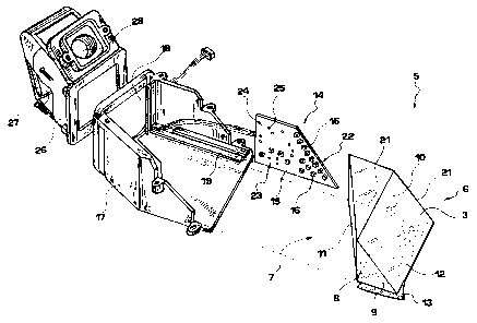
* figure 2 shows a partially exploded perspective
view of a detail of the device of figure 1; and
* figure 3 shows a perspective view of the detail
of figure 2 depicting the use thereof..
With reference to the figures, a device for the
taking and the reading of fingerprints is generally
indicated as 1. This version of device is
substantially portable and suitable to be
connected, as a peripheral, to a computer for
treating, storing and comparing the fingerprint.
However, it is understood that what is described in
the following can be referred to any device able to
carry out the function of taking fingerprints, e.g.
a device for generating the required data for an
electronic passport or for an electronic identity
card, a fixed check point and so on.
The device 1 of the present embodiment comprises a
case 2 substantially hand-grippable for an
operator, an impression surface 3 for fingerprints,
a starting button 4, and other possible reading
device of optical kind, RFID, a microchip reader
and the like.
The impression surface 3 corresponds to a first
surface of an anamorphic prism 5 of the device 1,
resulting from the matching of a first right-angled
triangular prism 6 and of a second right-angled
triangular prism 7, both having, as base polygon, a
right-angled triangle.
-4-
CA 02674192 2009-06-25
WO 2008/080995 PCT/EP2007/064652
In this kind of prism, as inclined surface it is
understood a surface, having greater width,
corresponding to the hypotenuse of the right-angled
triangle constituting the base of the prism. Said
impression surface 3 corresponds to a first
inclined surface of the first prism 6.
A first non-inclined surface 8 of the first prism 6
corresponds to a respective and non-inclined
surface of the second prism 7.
Said first inclined surface 3 extends between a
first triangular base 9 of its prism 6 and a plane
surface resulting from the matching of the
triangular base opposite to said first base, and a
second non-inclined surface of the second prism 7.
Said plane surface 10 hence has the shape of a
right-angled trapezium. The second inclined surface
of the anamorphic prism 5, belonging to the second
prism 7 and opposite to the first inclined surface
3, constitutes the taking and reading surface 11 of
the anamorphic prism 5.
The second non-inclined surface 12 of the first
prism 6, adjacent to the impression surface 3,
forms a further right-angled trapezium with the
base of the second prism 7.
Said second non inclined surface 12 of the first
prism 6, i.e. a surface adjacent to the impression
surface of the anamorphic prism 5, is treated in
such a way to shows a layer directed toward the
inside of the prism 5 having a reduced
reflectivity.
-5-
CA 02674192 2009-06-25
WO 2008/080995 PCT/EP2007/064652
In this embodiment, the surface 12 is treated
overlapping a high emissivity layer 13. In
particular, such layer 13 can have an light
absorption close to one, i.e. a reflectivity close
to zero, equivalent to that of a black body
incapable of reflecting light.
However, it is understood that these optical
characteristics should be valid at least for the
operational wavelengths of the device 1, i.e.
greater than 700 nm (infrared field).
At the plane surface 10, in a lateral position with
respect to the impression surface 3, the device 1
comprises a light source, indicated in general as
15, embodied by a printed circuit board on which a
plurality of first LEDs 16 are mounted,
electrically supplied in a conventional manner.
Said printed circuit board 15 is plane, having a
shape overlapping that of the plane surface 10.
Such printed circuit board 15 and the anamorphic
prism 5 are housed in a first case 17 leaving
uncovered the impression surface 3 and containing
the taking surface 11, in front of which a first
opening 18 is formed. Moreover, a positioning rail
19 is provided for the printed circuit board 15.
From the arrangement of the first LEDs 16 on the
printed circuit board it is understood that the
illumination is more intense at the lateral margin
20 of the impression surface 3, and at the vertex
of the plane surface 10, where a first set 22 of
LEDs 16 is placed. A second set 23 of LEDs 16 is
-6-
CA 02674192 2009-06-25
WO 2008/080995 PCT/EP2007/064652
placed at the lower margin 21 of the plane surface
on the second prism 7.
On the printed circuit board 15 a third set 24 of
second LEDs 24 is also provided, having a different
5 colouring with respect to that of the first LEDs 16
and intended to be switched on for signalling the
operation of the device 1 through the impression
surface 3.
The plane surface 10, wherein the light source is
10 placed, is satinized, so as to improve the light
diffusion inside the prism 5.
A second case 26 is connected to the first case 17
at the opening 18. The second case 26 contains a
reflecting surface 27 reflecting the image formed
over the taking and reading surface 11 toward a
second opening 28, housing lenses 29 (figure 3)
operating as filter, a filtering layer being
deposited on them, in particular on the surface of
the first or only lens receiving the light beam.
In the preset embodiment, the first LEDs are of the
IRLED type, i.e. they emit an infrared radiation
having a wavelength greater than 700 nm. Thus, said
filtering layer will have a bandwidth for
wavelengths greater than 700 nm.
The device 1 comprises, at said second opening, a
digital optical sensor, not shown, digitalizing the
image of the fingerprint. The sensor is of the CCD
type, or even of the CMOS type.
With reference to the device herein described, in
the following an embodiment of the method according
-7-
CA 02674192 2009-06-25
WO 2008/080995 PCT/EP2007/064652
to the invention will be detailed.
In such a method, an anamorphic prism 5 is provided
as above described, on which a first surface is
provided, in particular an inclined surface of the
prism, for having a fingerprint impressed on it by
a simple fingertip pressure.
On a surface adjacent to said first surface, a
layer having a reduced reflectivity is provided,
preferably having a light absorption coefficient
close to one, and said first surface is laterally
illuminated.
Then, the image of the fingerprint on a further
surface of the anamorphic prism is taken, opposite
to said first surface 3.
Nin the method according to the present embodiment,
the lighting is more intense at a lateral margin of
said first surface, and at the prism vertex at said
first surface.
The lighting is carried out by an infrared
radiation.
To the above device and method a man skilled in the
art, to comply with further and contingent
requirements, will adopt several further variations
and modifications, in any case all falling within
the protection scope of the present invention, as
defined by the annexed claims.
-8-