Note: Descriptions are shown in the official language in which they were submitted.
CA 02676948 2009-08-26
1
An array antenna comprising means to suppress the coupling effect in
the dielectric gaps between its radiator elements without establishing
galvanic contacts
The present invention relates to an apparatus for suppressing the
coupling effect in the dielectric gaps between the radiator elements of an
array antenna, without establishing galvanic contacts. For example, the
invention is particularly applicable to antenna modules for radar and telecom.
Nowadays radar systems may use a scanning phased array
antenna to cover their required angular range. Such an antenna comprises a
large number of identical radiator elements assembled onto a panel so as to
form a grid of radiator elements. The control of the phase shifting between
adjacent radiator elements enables to control the scanning angle of the beam
emitted by the array antenna. The techniques that are the most commonly
used to build an array antenna are based on interconnect substrate
technologies, e.g. the Printed Circuit Board technology (PCB). These thick-
film or thin-film multilayer technologies consist in many sequential steps of
laminating layers, of drilling holes through the layers and of metallizing the
holes. These sequential build-up technologies typically result in planar
interconnect devices comprising multiple interconnection layers. However,
the next generation of compact scanning phased array antennas require
Radio-Frequency (RF) radar functionalities to be implemented directly at the
antenna face, such as Active Electronically Scanned Array (AESA) antennas
for example. This cannot be achieved by the above mentioned techniques,
as they typically result in planar interconnect devices that do not afford
extra
room to embed the required RF components. This is one of the technical
problems that the present invention aims at solving.
The use of 3D-shaped radiator elements, so-called radiator
packages, may afford sufficient extra interior room. It is worth noting that a
3D radiator package also yields design possibilities in terms of bandwidth
and scan-angle that a planar device radiator cannot. The general aspect of a
radiator package is that of a hollowed box topped by an integrated antenna.
A large number of freestanding radiator packages are assembled onto a PCB
CA 02676948 2009-08-26
2
so as to form a grid of radiator packages, by picking and placing them onto
the board as surface mounted devices (SMD). So-called "unit cells" are used
as footprints to mount the radiator packages onto the PCB. A unit cell
determines the space available for each radiator package onto the PCB. The
width and the length of a unit cell is determined by the type of grid
(rectangular grid or triangular grid) and by the required performance, in
terms
of free space wavelength and of scanning requirements. Units cells are
printed at the surface of the PCB according to a triangular grid pattern or a
rectangular grid pattern, thus providing a convenient mean to arrange the
radiator packages onto the PCB. Unfortunately, gaps are left between the
radiator packages. The depth of these gaps is equal to the height of a unit
cell, which is determided by the dimensions and the layout of the RF
components that must be embedded inside the radiator elements.
Consequently, the depth of the gaps cannot be adjusted.
Basically, these gaps result from the necessary tolerances
required by the process of placing and assembling the radiator packages.
Practically, the width of the gaps can be limited to a minimum, as long as it
allows for placement on the PCB and as long as it allows for thermal
expansion and cooling of the radiator packages. Thus, doing without the
gaps is not workable. Unfortunately, these "mechanical gaps" incidently form
"RF gaps" or "dielectric gaps" behaving like waveguides, into which the
electromagnetic energy radiated by the packages partly couples. Reflected in
the bottom of the gaps by the PCB, undesired interference with the directly
emitted energy into free space are generated. Depending on the height of the
radiator packages and on the wavelength, the gaps may induce mismatch
scanning problems for some of the required scanning angle, for example the
scanning angles up to 60 degrees in all directions. This is another technical
problem that the present invention aims at solving. It is worth noting that,
in a
large bandwidth antenna, minimizing the width of the gaps may only alleviate
the problem. Minimizing the width of the gaps cannot solve the problem.
An existing solution consists in an array of radiator packages
attached to a board by means of conducting bolts. The boltheads short-circuit
the conductive sidewalls of the adjacent radiator packages by virtue of
CA 02676948 2009-08-26
3
contact shims, thus suppressing undesired waveguide modes inside the
gaps. However, if the array antenna comprises a lot of radiator packages,
this solution leads to a very complex assembly, which is bound to hamper
any later maintenance or repair operation. Actually, removing an individual
radiator element may turn into a challenge in regard of the very high level of
integration of nowadays systems, as it implies unscrewing several bolts with
special tools and handling with tiny shims. Another major disadvantage of
this solution is that the use of bolts inserted between the radiator elements
do
not allow for proper thermal expansion, thus requiring the use of an
additional
high-performance cooling system. These are other technical problems that
the present invention aims at solving.
In an attempt to provide a radar system that requires little room
whereas the radiator packages are easily interchangeable for maintenance or
repair work, the US patent No. US 6,876,323 discloses a radar system with a
phase-controlled antenna array. The disclosed system comprises a plurality
of data and supply networks interchangeably arranged and a plurality of
transmit/receive modules (e.g.: 3D radiator packages) arranged
interchangeably on a radiation side of the radar system. The sender/receiver
modules are said to be exchangeable either from the irradiation side or from
the front side of the radar system equally. However, the disclosed system
comprises narrow gaps between the exchangeable sender/receiver modules,
these gaps necessarily behaving like waveguides into which the
electromagnetic energy radiated couples. Consequently, the system
disclosed in the US patent No. US 6,876,323 is not adapted to angular
scanning.
The present invention aims to provide an apparatus which may be
used to overcome at least some of the technical problems described above.
The present invention provides a virtual reflecting boundary, which
suppresses electromagnetic fields in the gaps between the radiator
packages, without the need for galvanic contacts between the individual
radiator packages. At its most general, the present invention described
hereafter may provide an apparatus comprising a plurality of three-
dimensional radiator elements, each radiator element transmitting or
CA 02676948 2016-05-04
4
receiving electromagnetic waves by its radiating top side. The radiator
elements are arranged so that their radiating top sides are parallel and so
that at least one pair of adjacent radiator elements are separated by a
dielectric gap between sidewalls, the gap behaving like a waveguide which
induces by a coupling effect electromagnetic interferences with the waves.
Each of said adjacent radiator elements comprises means to suppress the
coupling effect without establishing a galvanic contact with its adjacent
radiator element.
In a preferred embodiment, the means to suppress the coupling
effect may comprise corrugations arranged at the sidewall facing the gap, the
corrugations being arranged so as to interlace with the corrugations of the
adjacent radiator element, without establishing a mechanical contact.
Advantageously, the sidewall facing the gap and its corrugations
may be metallized.
For example, the three-dimensional radiator elements may be
mounted onto a printed circuit board by their bottom sides opposite to their
radiating top sides, the radiating top sides being in a same plan so as to
form
an array of three-dimensional radiator elements.
For example, the three-dimensional radiator elements may be all
identical, arranged so as to form an array of the triangular type.
Advantageously, the corrugations may be orthogonal to the
radiating top sides, so that each radiator element can be independently
picked out from the printed circuit board.
For example, the array of three-dimensional radiator elements
may be part of a scanning phased array antenna.
According to an aspect of the present invention, there is provided an
apparatus comprising a plurality of three-dimensional radiator elements, each
radiator element transmitting or receiving electromagnetic waves by its top
side
which comprises a radiating patch antenna, the radiator elements being
arranged
so that their radiating top sides are in a same plane and so that at least one
pair
of adjacent radiator elements are separated by a gap between sidewalls, the
gap
behaving like a waveguide which induces by a coupling effect electromagnetic
interferences with the waves, each of said adjacent radiator elements
comprises
means to suppress the coupling effect without establishing a galvanic contact
with
its adjacent radiator element, these means comprising corrugations arranged at
the sidewall facing the gap, the corrugations being arranged so as to
interlace
CA 02676948 2016-05-04
4a
with the corrugations of the adjacent radiator element, without establishing a
mechanical contact.
In any of its aspects, the invention disclosed herein conveniently
provides a true pick and place solution of the SMD type, which enables to
easily assemble individual 3D radiator packages together in an array
configuration. It allows for easy placement of the 3D radiator packages on a
PCB, for thermal expansion and for cooling. Implemented in a scanning
phased array antenna, it allows for large scan angles without mismatch
scanning problems and it allows for large bandwidth performance.
CA 02676948 2009-08-26
Exchanging an individual 3D radiator element does not require an unusual
effort, especially because the radiator elements are not in contact.
A non-limiting exemplary embodiment of the invention is described
5 below with reference to the accompanying drawings in which:
- the figure 1 schematically illustrates by a perspective view an
exemplary 3D radiator package with corrugations according to the
invention;
- the figure 2 schematically illustrates by a perspective view an
exemplary 4x4 array of 3D corrugated radiator packages according
to the invention;
- the figure 3 schematically illustrates by a perspective view an
exemplary virtual reflecting boundary provided by the invention.
Figure 1 schematically illustrates by a perspective view an
exemplary 3D radiator package 1, which may emit and/or receive
electromagnetic waves. The radiator package 1 may be fabricated by
different technologies. For example, LTCC technology (Low-Temperature,
Cofired Ceramic) or 3D MID technology (3-Dimensional Molded Interconnect
Device technology) are suitable. The radiator package 1 comprises at its
radiating top side 14 a patch antenna 11. In the illustrated embodiment, the
four sidewalls of the radiator package 1, including a sidewall 12 and a
sidewall 13, may advantageously be corrugated. A parallelepiped-shaped
corrugation 10 may be arranged at the sidewall 12, its longitudinal axis being
advantageously orthogonal to the radiating top side 14. Two parallelepiped-
shaped corrugations 4 and 5 may be arranged at a sidewall opposite to the
sidewall 12, not viewable on Figure 1, their longitudinal axis being
advantageously orthogonal to the radiating top side 14. The corrugations 10
may be sized and arranged so as to be facing the space between the
corrugations 4 and 5 on the opposite sidewall. Four parallelepiped-shaped
corrugations 6, 7, 8 and 9 may be arranged at the sidewall 13, their
longitudinal axis being advantageously orthogonal to the radiating top side
14. Two parallelepiped-shaped corrugations 2 and 3 may be arranged at a
sidewall opposite to the sidewall 13, not viewable on Figure 1, their
CA 02676948 2009-08-26
6
longitudinal axis being advantageously orthogonal to the radiating top side
14. The corrugations 2 may be sized and arranged so as to be facing the
space between the corrugations 8 and 9 on the opposite sidewall. The
corrugations 3 may be sized and arranged so as to be facing the space
between the corrugations 6 and 7 on the opposite sidewall. Advantageously,
the four sidewalls of the radiator package 1 may be metallized, including the
corrugations 2, 3, 4, 5, 6, 7, 8, 9 and 10. In the illustrated embodiment,
combining in an array several 3D radiator packages identical to the radiator
package 1 may advantageously result in interlacing the metallized
corrugations of adjacent radiator packages, so as to form a structure crept
into the dielectric gap between the adjacent radiator packages, as illustrated
by Figure 2. The so-formed crept structure enables to solve the problem of
detrimental scanning mismatch due to the dielectric gap between
freestanding 3D radiator packages, when 3D radiator packages are
combined in an array antenna for example.
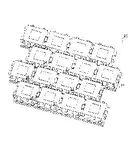
Figure 2 schematically illustrates by a perspective view an
exemplary 4x4 array 20 of sixteen 3D corrugated radiator packages identical
to the radiator package 1, advantageously arranged in a triangular grid onto a
PCB 21 according to the invention. For example, the radiator packages 1, 22,
23, 24, 25, 26 and 27 may be bonded onto the PCB 21 by their side opposite
to their radiating top side, so that their radiating top sides are
advantageously
in a same plan. For the sake of clarity, the same references 2, 3, 4, 5, 6, 7,
8,
9 and 10 are used to identify the metallized corrugations, independently from
the radiator package specifically considered. Advantageously, the metallized
corrugation 10 of the radiator package 1 may be sized and arranged so as to
allow easy interlacing with the metallized corrugations 4 and 5 of a single
adjacent radiator package 22. The metallized corrugations 2 and 3 of the
radiator package 1 may be sized and arranged so as to allow easy interlacing
with the metallized corrugations 6 and 7 of an adjacent radiator packages 23
and with the metallized corrugations 8 and 9 of an adjacent radiator package
24. The metallized corrugations 4 and 5 of the radiator package 1 may be
sized and arranged so as to allow easy interlacing with the metallized
corrugation 10 of a single adjacent radiator package 25. The metallized
CA 02676948 2009-08-26
7
corrugations 6, 7, 8 and 9 of the radiator package 1 may be sized and
arranged so as to allow easy interlacing with the metallized corrugation 2 of
an adjacent radiator packages 26 and with the metallized corrugation 3 of an
adjacent radiator packages 27. It is worth noting that the radiator package 1
is neither in contact with the radiator package 22, nor in contact with the
radiator package 23, nor in contact with the radiator package 24, nor in
contact with the radiator package 25, nor in contact with the radiator package
26, nor in contact with the radiator package 27. The radiator package 1 is
separated from those adjacent packages 22, 23, 24, 25, 26 and 27 by a non-
linear 'mechanical gap'. Hereby, the electromagnetic field must .meander into
the non-linear gap between the metallized corrugations, with a weaker
coupling than it would propagate in a linear gap.
Figure 3 schematically illustrates by a perspective view an
exemplary virtual reflecting boundary 30 provided by the invention. Actually,
the top of the corrugations acts like a virtual reflecting boundary, as if the
3D
radiator packages were galvanically connected at that level.
It is to be understood that variations to the example described
above, such as would be apparent to the skilled addressee, may be made
without departing from the scope of the present invention.
Conveniently, the invention disclosed herein leaves free choice of
the height of the 3D radiator packages to accommodate the RF components
at the inside of the radiator packages.