Language selection

Search

Patent 2678049 Summary

Third-party information liability

Some of the information on this Web page has been provided by external sources. The Government of Canada is not responsible for the accuracy, reliability or currency of the information supplied by external sources. Users wishing to rely upon this information should consult directly with the source of the information. Content provided by external sources is not subject to official languages, privacy and accessibility requirements.

Claims and Abstract availability

Any discrepancies in the text and image of the Claims and Abstract are due to differing posting times. Text of the Claims and Abstract are posted:

  • At the time the application is open to public inspection;
  • At the time of issue of the patent (grant).
(12) Patent: (11) CA 2678049
(54) English Title: BROADBAND RF CONNECTOR INTERCONNECT FOR MULTILAYER ELECTRONIC PACKAGES
(54) French Title: INTERCONNEXION PAR CONNECTEUR RF LARGE BANDE POUR BOITIERS ELECTRONIQUES MULTICOUCHES
Status: Granted and Issued
Bibliographic Data
(51) International Patent Classification (IPC):
  • H01R 24/44 (2011.01)
  • H01R 12/58 (2011.01)
  • H01R 13/6464 (2011.01)
(72) Inventors :
  • AGUIRRE, GERARDO (United States of America)
(73) Owners :
  • KYOCERA AMERICA, INC.
(71) Applicants :
  • KYOCERA AMERICA, INC. (United States of America)
(74) Agent: OYEN WIGGS GREEN & MUTALA LLP
(74) Associate agent:
(45) Issued: 2015-12-08
(86) PCT Filing Date: 2008-02-13
(87) Open to Public Inspection: 2008-08-28
Examination requested: 2012-11-20
Availability of licence: N/A
Dedicated to the Public: N/A
(25) Language of filing: English

Patent Cooperation Treaty (PCT): Yes
(86) PCT Filing Number: PCT/US2008/053880
(87) International Publication Number: US2008053880
(85) National Entry: 2009-08-13

(30) Application Priority Data:
Application No. Country/Territory Date
11/709,080 (United States of America) 2007-02-21

Abstracts

English Abstract

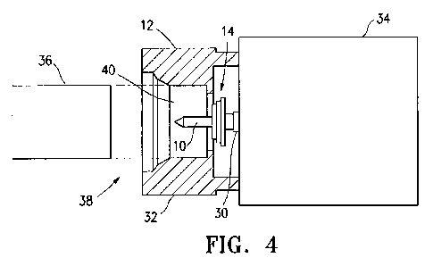
A coaxial transition arrangement including a coaxial connector for connecting a coaxial cable to a multilayer package has an improved coaxial connector for accomplishing impedance matching and providing improved broadband performance. Impedance matching is provided by a metal disk structure comprising a plurality of metal disks mounted on a center conductor pin of the coaxial connector. The disks are mounted in spaced-apart relation on the center conductor pin and have different radiuses which decrease with increasing distance from the base of the center conductor pin. The coaxial connector has a shroud which is configured to accommodate the metal disk structure therein, as does the ring of ground vias forming a part of the multilayer package.


French Abstract

Système de transition coaxial comportant un connecteur coaxial conçu pour connecter un câble coaxial à un boîtier multicouche, ledit connecteur coaxial présentant une conception améliorée assurant une adaptation d'impédance et une meilleure qualité de transmission en large bande. L'adaptation d'impédance est réalisée par une structure à disques métalliques comprenant une pluralité de disques métalliques montés sur une broche conductrice centrale du connecteur coaxial. Les disques sont montés espacés les uns des autres sur la broche conductrice centrale et possèdent des rayons différents qui diminuent à mesure que la distance qui les sépare de la base de la broche conductrice centrale augmente. Le connecteur coaxial est doté d'une coque configurée pour recevoir la structure à disques métalliques, à l'instar de la couronne de traversées d'interconnexion à la masse qui fait partie du boîtier multicouche.

Claims

Note: Claims are shown in the official language in which they were submitted.


I claim:
1. A coaxial connector having a center conductor pin surrounded by a
shroud, the connector having at least three conductive disks of different
size mounted contiguously in actual contact with each other on the
center conductor pin to provide impedance matching.
2. The coaxial connector set forth in claim 1, wherein the conductive disks
are comprised of relatively thin metal disks of different radii.
3. The coaxial connector set forth in claim 1, further including a
multilayer package having the coaxial connector mounted thereon.
4. The coaxial connector set forth in claim 3, wherein the multilayer
package includes a stack of ceramic layers and the center conductor pin
has a braze pad at a base thereof brazed to the stack of ceramic layers.
5. The coaxial connector set forth in claim 3, wherein the multilayer
package includes a ring of ground vias having an aperture therein for
receiving the center conductor pin therein.
6. The coaxial connector set forth in claim 3, further including a coaxial
cable connected to the coaxial connector.
7. A coaxial connector having a center conductor pin surrounded by a
shroud, the connector having a plurality of conductive disks of different
outer radius mounted in spaced-apart fashion on the center conductor
pin to provide impedance matching, further including a multilayer
package having the coaxial connector mounted thereon, wherein the
center conductor pin has a base thereof mounted on the multilayer
package and the plurality of conductive disks comprise three metal
7

disks which have decreasing diameters with increasing distance from
the multilayer package.
8. A coaxial transition arrangement comprising the combination of:
a multilayer package;
a coaxial cable; and
a coaxial connector coupling the multilayer package to the coaxial
cable, the coaxial connector including a center conductor pin having a
metal disk structure thereon, the metal disk structure comprising at
least three metal disks mounted contiguously in actual contact with
each other along the conductor pin and providing impedance matching.
9. The coaxial transition arrangement set forth in claim 8, wherein the
center conductor pin has a base coupled to the multilayer package and
the metal disks have decreasing diameters with increasing distance
from the multilayer package.
10. The coaxial transition arrangement set forth in claim 8, wherein the
coaxial connector includes a shroud mounted on the multilayer package,
surrounding the center conductor pin and the metal disk structure
thereon and receiving the coaxial cable therein.
8

Description

Note: Descriptions are shown in the official language in which they were submitted.


CA 02678049 2009-08-13
WO 2008/103588 PCT/US2008/053880
BROADBAND RF CONNECTOR INTERCONNECT
FOR MULTILAYER ELECTRONIC PACKAGES
Background of the Invention
1. Field of the Invention
[0001] The present invention relates to a broadband RF connector
interconnect for multilayer electronic packages, and more particularly to
impedance matching to provide improved broadband performance in ceramic
multilayer packages requiring brazed connectors.
2. History of the Prior Art
[0002] It is known in the art to provide a coaxial transition arrangement
including a broadband RF connector interconnect for multilayer electronic
packages. Such arrangements are commonly used in, for example, radar systems
having an electronic package with a transmit/receive module and antenna feed
network for the transmitter.
[0003] In such arrangements, it is difficult to achieve broadband high
frequency RF performance from a coaxial connector transition to a transmission
line structure within a multilayer package. It is impossible to compensate the
impedance mismatch within the connector by using impedance matching
structures inside the package alone. Attempts to compensate connector
transition
by reducing the braze pad for the pin connection leads to high-risk
manufacturing
and connector reliability.
[0004] Various different arrangements have been tried in an attempt to
provide impedance matching and thereby broadband performance in coaxial
transition arrangements. Such an arrangement is shown in U.S. Patent 3,745,488
of Rogers. This patent describes a disk 70 and a ring 78 which are moveable
within a coaxial structure to achieve impedance matching. However, such
structure is relatively complex and not readily adapted to coaxial transition
arrangements which couple a coaxial cable to a multilayer package so that
impedance matching is achieved with minimum modification. Similar comments

CA 02678049 2009-08-13
WO 2008/103588 PCT/US2008/053880
apply to U.S. Patent 6,02$,497 of Allen in which the impedance of a coaxial
transmission line is adjusted by adjusting the width and shape of a pin and
the
inner diameter of a washer-shaped end of a shroud.
Brief Description of the Invention
[0005] The present invention provides impedance matching and improved
broadband performance with a broadband RF connector interconnect for
multilayer electronic packages in which only relatively minor modification of
conventional structures is required. A coaxial transition arrangement
comprises a
transmission line structure inside a multilayer package, a coaxial cable and a
coaxial connector coupling the multilayer package to the coaxial cable. The
coaxial
conductor includes a center conductor pin having a metal disk structure
thereon.
The metal disk structure provides impedance matching.
[0006] In accordance with the invention, the metal disk structure includes a
plurality of metal disks of different size mounted in spaced-apart relation
along
the center conductor pin. The center conductor pin has a base coupled to the
multilayer package, and the plurality of metal disks have decreasing diameters
with increasing distance from the multilayer package. The coaxial connector
includes a shroud brazed on the multilayer package, surrounding the center
conductor pin and the metal disk structure thereon and receiving the coaxial
cable
therein.
[0007] In a preferred arrangement according to the invention, the
multilayer package includes a stack of ceramic layers, inside which a coaxial
via
structure exists. The center conductor pin of the broadband RF connector has a
braze pad at a base thereof which is brazed to the stack of the ceramic
layers.
Within the ceramic layers the center via of the coaxial structure is connected
to
the braze pad. The multilayer package may include a ring of ground vias for
construction of coaxial via structure.
[0008] Impedance matching in accordance with the invention is achieved
with only relatively minor modification of conventional coaxial structures.
More
specifically, a plurality of the thin metal disks are mounted on the center
2

CA 02678049 2009-08-13
WO 2008/103588 PCT/US2008/053880
conductor pin adjacent the braze pad at the base of the pin. Additionally, the
size
and shape of a shroud which surrounds the center conductor pin is adjusted so
as
to accommodate the thin conductive disks.
[0009] In a preferred arrangement, three conductive disks are mounted on
the center conductor pin in spaced-apart relation adjacent the braze pad of
the pin.
The diameter of each disk is different from the diameter of the other two
disks,
and the disks are mounted such that the diameters thereof decrease with
increasing distance from the braze pad.
Brief Description of the Drawings
[0010] FIG. 1 is a perspective, exploded view of a center conductor pin of a
coaxial connector showing the manner in which plural conductive disks are
mounted on the center connector pin to achieve impedance matching in
accordance
with the invention.
[0011] FIG. 2 is a side view of the center conductor pin of FIG. 1 showing
the disks mounted thereon in accordance with the invention.
[0012] FIG. 3 is a side sectional view of a coaxial connector in which the
center conductor pin of FIGS. 1 and 2 is mounted within a surrounding shroud.
[0013] FIG. 4 is a side sectional view of the coaxial connector of FIG. 3
showing the manner in which it is coupled to a multilayer package and the
manner in which it receives a coaxial cable, to provide a coaxial transition
arrangement.
[0014] FIG. 5 is a side sectional view of a coaxial transition arrangement
similar to that shown in FIG. 4, in which the coaxial structure within the
multilayer package includes an iris and a ring of grounded vias.
[0015] FIG. 6 is a plan view of the ground ring and iris of FIG. 5.
[0016] FIG. 7 is a side sectional view similar to that of FIG. 5 and showing
the manner in which the ground ring has the coaxial connector coupled thereto.
[0017] FIG. 8 is a diagrammatic plot of S-parameter magnitude in dB as a
function of frequency in GHz for a conventional coaxial transition
arrangement,
3

CA 02678049 2009-08-13
WO 2008/103588 PCT/US2008/053880
without the impedance matching conductive disks, and showing reflection loss
or
return loss, and also insertion loss.
[0018] FIG. 9 is a diagrammatic plot similar to that of FIG. 8 but with the
conducti.ve disks mounted on the center conductor pin to provide impedance
matching in accordance with the invention.
Detailed Description
[0019] FIG. 1 is an exploded perspective view of a center conductor pin 10 of
a coaxial connector 12 having a metal disk structure 14 mounted on the pin 10
to
provide impedance matching in accordance with the invention. The metal disk
structure 14 includes three different disks 16, 18 and 20, each with a radius
different than that of the other two disks. The disk 16 has a radius which is
larger
than the disk 18. The disk 18, in turn, has a radius which is larger than that
of
the disk 20.
[0020] The center conductor pin 10 is of conventional design and has a
generally cylindrical portion 22 which terminates in a tip 24. The center
conductor
pin 10 has a second cylindrical portion 26 of diameter which is larger than
the
diameter of the cylindrical portion 22. The second cylindrical portion 26
extends
between the first cylindrical portion 22 and a base 28 of the center conductor
pia.a
on which a braze pad 30 is mounted.
[0021] As shown in the side view of FIG. 2, the disks 16, 18 and 20 are
mounted in spaced-apart relation along the second cylindrical portion 26 of
the
center conductor pin 10 adjacent the braze pad 30. The disks 16, 18 and 20 are
of
varying radii and are located such that the disk 16 is closest to the braze
pad 30,
the disk 18 of diameter slightly smaller than that of the disk 16 is mounted
on the
other side of the disk 16 from the braze pad 30, and the disk 20 of diameter
slightly smaller than that of the disk 18 is mounted on the other side of the
disk 18
from the disk 16.
[0022] The center conductor pin 10 with the metal disk structure 14
thereon form a part of the coaxial connector 12 which is shown in FIG. 3. The
4

CA 02678049 2009-08-13
WO 2008/103588 PCT/US2008/053880
center conductor pin 10 is concentrically disposed within and is surrounded by
a
shroud 32. The shroud 32 is of conventional design except that it is enlarged
as
necessary to accommodate the metal disk structure 14 on the center conductor
pin
10.
[0023] FIG. 4 shows the coaxial connector 12 of FIG. 3 mounted on a
multilayer package 34 and receiving a coaxial cable 36 so as to provide a
coaxial
transition arrangement 38 between the multilayer package 34 and the coaxial
cable 36. The center conductor pin 10 of the coaxial connector 12 is coupled
to the
multilayer package by way of the braze pad 30 at the base thereof. The braze
pad
30 is brazed to the multilayer package 34. The shroud 32 is also coupled to
the
multilayer package 34, as shown in FIG. 4. The multilayer package 34 may
comprise a stack of ceramic layers.
[0024] The shroud 32 has an opening 40 therein for receiving the coaxial
cable 36 to couple the coaxial cable 36 to the multilayer package 34 by way of
the
coaxial connector 12.
[0025] The transmission line structure within the multilayer package 34
may comprise a coaxial via structure, as in the case of the present example,
or it
may comprise a slabline structure or a stripline structure. FIG. 5 shows the
coaxial cable 36 coupled to the coaxial connector 12 which is mounted on the
multilayer package 34 including a ground ring 42 which is connected to a
circular
arrangement of grounded vias 44. The ground ring 42, which is shown in FIG. 6
as well as FIGs. 5 and 7, has an iris opening 46 therein for accommodating the
center conductor via of the coaxial structure within the multilayer package.
[0026] As previously noted, the metal disk structure 14 consisting of the
disks 16, 18 and 20 on the center conductor pin 10 provides impedance matching
with the result that improved broadband performance is achieved. This is
illustrated by the diagrammatic plots in FIGs. 8 and 9. FIG. 8 is a plot of
S-parameter magnitude in dB as a function of frequency/GHz for a conventional
coaxial connector. An upper curve 50 is insertion loss, and a lower curve 52
is
reflected loss or return loss. As shown in FIG. 8, the upper curve 50
representing
5

CA 02678049 2009-08-13
WO 2008/103588 PCT/US2008/053880
insertion loss deviates from the zero axis at a frequency of approximately 20
GHz
indicating that the performance of the conventional coaxial connector is
considerably less than ideal.
[0027] FIG. 9 is a diagrammatic plot similar to that of FIG. 8 but
representing the performance provided by the coaxial connector 12 with the
metal
disk structure 14 according to the present invention. An upper curve 54
represents insertion loss, and a lower curve 56 represents reflected loss or
return
loss. As will be seen from FIG. 9, in the case of the coaxial connector 12
according
to the invention, the insertion loss represented by the curve 54 remains at
zero up
to a frequency of approximately 32 GHz, representing far better performance
than
in the case of the conventional coaxial connector illustrated by the plot of
FIG. 8.
The improved performance is due to the impedance matching provided by the
metal disk structure 14.
6

Representative Drawing
A single figure which represents the drawing illustrating the invention.
Administrative Status

2024-08-01:As part of the Next Generation Patents (NGP) transition, the Canadian Patents Database (CPD) now contains a more detailed Event History, which replicates the Event Log of our new back-office solution.

Please note that "Inactive:" events refers to events no longer in use in our new back-office solution.

For a clearer understanding of the status of the application/patent presented on this page, the site Disclaimer , as well as the definitions for Patent , Event History , Maintenance Fee  and Payment History  should be consulted.

Event History

Description Date
Common Representative Appointed 2019-10-30
Grant by Issuance 2015-12-08
Inactive: Cover page published 2015-12-07
Inactive: Adhoc Request Documented 2015-10-06
Inactive: Delete abandonment 2015-10-06
Deemed Abandoned - Conditions for Grant Determined Not Compliant 2015-08-10
Pre-grant 2015-07-08
Inactive: Final fee received 2015-07-08
Notice of Allowance is Issued 2015-02-10
Letter Sent 2015-02-10
Notice of Allowance is Issued 2015-02-10
Inactive: Q2 passed 2014-12-15
Inactive: Approved for allowance (AFA) 2014-12-15
Amendment Received - Voluntary Amendment 2014-07-22
Inactive: S.30(2) Rules - Examiner requisition 2014-03-05
Inactive: Report - No QC 2014-02-28
Inactive: IPC deactivated 2013-11-12
Inactive: <RFE date> RFE removed 2013-05-31
Letter Sent 2013-05-31
Inactive: Delete abandonment 2013-05-31
Inactive: First IPC assigned 2013-02-27
Inactive: IPC assigned 2013-02-27
Inactive: Abandon-RFE+Late fee unpaid-Correspondence sent 2013-02-13
Request for Examination Received 2012-11-20
Request for Examination Requirements Determined Compliant 2012-11-20
Inactive: Adhoc Request Documented 2012-11-20
All Requirements for Examination Determined Compliant 2012-11-20
Inactive: IPC expired 2011-01-01
Inactive: IPC assigned 2010-11-16
Inactive: IPC removed 2010-11-16
Inactive: First IPC assigned 2010-11-16
Inactive: IPC assigned 2010-11-16
Inactive: IPRP received 2010-01-28
Inactive: Office letter 2010-01-13
Letter Sent 2010-01-13
Inactive: Single transfer 2009-11-06
Inactive: Declaration of entitlement - PCT 2009-11-06
Inactive: Cover page published 2009-11-06
IInactive: Courtesy letter - PCT 2009-10-09
Inactive: Notice - National entry - No RFE 2009-10-09
Application Received - PCT 2009-10-07
National Entry Requirements Determined Compliant 2009-08-13
Application Published (Open to Public Inspection) 2008-08-28

Abandonment History

Abandonment Date Reason Reinstatement Date
2015-08-10

Maintenance Fee

The last payment was received on 2014-10-22

Note : If the full payment has not been received on or before the date indicated, a further fee may be required which may be one of the following

  • the reinstatement fee;
  • the late payment fee; or
  • additional fee to reverse deemed expiry.

Patent fees are adjusted on the 1st of January every year. The amounts above are the current amounts if received by December 31 of the current year.
Please refer to the CIPO Patent Fees web page to see all current fee amounts.

Owners on Record

Note: Records showing the ownership history in alphabetical order.

Current Owners on Record
KYOCERA AMERICA, INC.
Past Owners on Record
GERARDO AGUIRRE
Past Owners that do not appear in the "Owners on Record" listing will appear in other documentation within the application.
Documents

To view selected files, please enter reCAPTCHA code :


To view images, click a link in the Document Description column. To download the documents, select one or more checkboxes in the first column and then click the "Download Selected in PDF format (Zip Archive)" or the "Download Selected as Single PDF" button.

List of published and non-published patent-specific documents on the CPD .

If you have any difficulty accessing content, you can call the Client Service Centre at 1-866-997-1936 or send them an e-mail at CIPO Client Service Centre.


Document
Description 
Date
(yyyy-mm-dd) 
Number of pages   Size of Image (KB) 
Description 2009-08-12 6 273
Drawings 2009-08-12 3 44
Abstract 2009-08-12 1 61
Claims 2009-08-12 2 57
Representative drawing 2009-11-05 1 6
Claims 2009-08-13 2 63
Claims 2014-07-21 2 67
Notice of National Entry 2009-10-08 1 193
Courtesy - Certificate of registration (related document(s)) 2010-01-12 1 125
Reminder - Request for Examination 2012-10-15 1 117
Acknowledgement of Request for Examination 2013-05-30 1 190
Commissioner's Notice - Application Found Allowable 2015-02-09 1 162
PCT 2009-08-12 4 127
Correspondence 2009-10-08 1 21
Correspondence 2009-11-05 2 79
Correspondence 2010-01-12 1 16
PCT 2009-08-13 8 394
Final fee 2015-07-07 2 59