Note: Descriptions are shown in the official language in which they were submitted.
CA 02678298 2009-09-04
-1-
Title: METHOD AND APPARATUS FOR IDENTIFYING AN
ELECTRICAL DEVICE
FIELD OF THE INVENTION
This invention relates generally to the field of electronics, and more
particularly to the field of electronic or electro-mechanical devices. Most
particularly this invention relates to identifying such devices through the
use of individual identification and/or lot tracking information.
BACKGROUND OF THE INVENTION
Tracking and identifying devices is an important issue in modern
commerce, especially with respect to manufactured goods. Identification
of goods means that the source of the goods can be verified, and if the
device can be identified, its distribution and location can be tracked for
inventory, sales, product liability or many other purposes. For example, a
unique identification number can be used to ensure that the device
originates from the legitimate manufacturer and therefore is not a
counterfeit or knock off.
A number of identification or tracking systems have been
developed and are well known. One such tracking device is the use of
bar code labels that are read optically with a scanner. This system is
used extensively in retail establishments and among other things
simplifies pricing goods at checkout and inventory tracking. While this
technology is very useful and cost effective, it relies on a printed label
being affixed to the outside of the product and requires an optical scanner
to read the bar code. Often the bar code label is applied in the
supermarket of the like, or it might be incorporated into the printing of the
label on the product. Such bar code labels are highly visible and can be
removed or damaged and thus the tracking can be rendered inoperative.
Another known tracking and identification technology is through the
use of RFID tags, which may also be attached to the outside of the object
CA 02678298 2009-09-04
-2-
being tracked. RFID tags are also very useful, but may have some
disadvantages, such as, that some versions of the RFID tags can be
remotely scanned and tracked, which may be considered an invasion of
privacy. Also, RFID tags, like bar code labels, are separate items that are
attached to the object and thus can be removed, whether intentionally or
unintentionally, rendering any further tracking impossible. In other words,
once the RFID tag is removed, it may be difficult to say, for example, if the
product is a real or genuine product, or a knock off. Preventing the
proliferation of knock-off and counterfeit products is a critical concern for
trademark owners and product developers.
As can now be appreciated each of these known tracking systems
require the addition to a device to be tracked of a separate label or tag
which forms the basis of the identification. This makes such tracking
systems universally applicable to any type of good or object that has a
place onto which the tag or label may be affixed, regardless of the
character of the object, but also requires the addition to the object of the
tag or label.
Another way of tracking items relies on electromagnetic radiation.
For example, in US patent 4,333,072 to Beigel, a close coupled
identification system is disclosed for identifying an animal object or other
thing. A probe is provided including a circuit connected to a source of
alternating current, and a separate miniature circuit is adapted to be
implanted or attached to the animal object or thing. The probe circuit,
when held close to the implanted circuit, inductively couples the circuits so
that a load applied to the implanted circuit has an affect on the current in
the probe circuit. A programmable load is included in the implant circuit
along with a means for connecting and disconnecting the load, in
response to the alternating current cycles in the probe circuit according to
a predetermined code program. A signal is derived from the probe circuit
corresponding to the coded program in the implant circuit and the signal is
decoded and displayed as a number or other representation to indicate
CA 02678298 2009-09-04
-3-
the identity of the object.
While interesting, this device has a probe which relies on
electromagnetic radiation powered by an alternating current. Further, the
device requires a separate implant circuit, which is like a label of the other
methods and is to be affixed to the object or implanted into an animal.
The coding is achieved by alternately loading and unloading the receiver
coil in the implant circuit, and the implant circuit is designed to load and
couple to the probe's electromagnetic field. To minimize the size of the
implant circuit, the patent teaches there is no battery or other power
source on the implant circuit. Further, while some objects can have tags
implanted or affixed to them, other objects are not amenable to a separate
element being added as required by all of the foregoing prior art
technologies.
What is desired is a method and an apparatus for identifying
objects that do not require, or cannot accommodate, the addition of a
physically separate label or tag to the object to be identified, and which
therefore eliminate the cost associated with the physically separate tag
from the tracking system. Most preferably the identification system would
also not be visible and thus would be much more difficult to tamper with,
remove, or obscure.
SUMMARY OF THE INVENTION
The present invention is directed to a method and an apparatus for
providing an identification system that does not require physically affixing
a separate label or tag, to either the exterior, or the interior, of any other
part of the object to be tracked. The present invention is directed to an
identification system that is limited to use on a certain type of device,
namely a device having an electrical load and a controller for controlling
power to the electrical load. The present invention is preferred to be
capable of assigning to each object a separate and unique identifying
code, which can be translated into a self generated electromagnetic pulse
CA 02678298 2009-09-04
-4-
sequence within the object, and then detected by means of a close
proximity probe. In this way the present invention provides identification
for an object through a means that is not visible and requires no physically
separate tag or label to be affixed to the object. Thus, an advantage of
the present invention is the elimination of the individual unit cost of such
physically separate tags or labels. Most preferable the present invention
relies on a controller to selectively connect an electrical load to a source
of power to generate a digital electromagnetic signal, which can be
detected by a passive probe positioned within the electromagnetic field, in
proximity to the object. The controller can be a CPU, micro-controller, ,
micro-processor, Field Programmable Gate Array (FPGA), digital logic
controller, or the like. The present invention provides an identification
system which is not visible to the naked eye and thus is much less prone
to be obliterated or destroyed or added to illegally manufactured goods.
Furthermore, the absence of the identification code will be a clear
indication that the object is not a legitimate good.
Therefore, according to one aspect, the present invention provides
a method of identifying an electrical device, comprising the steps of:
providing an identification code to a controller;
operatively connecting said controller to an electrical load;
using said controller to create a sequence of timed electromagnetic
field pulses in accordance with said identification code;
said sequence of timed electromagnetic field pulses comprising an
initial pulse followed by one or more pulse groups, each pulse group
consisting of a time delay followed by at least one subsequent pulse;
detecting said sequence of timed pulses by means of a passive
probe; and
translating said sequence of timed pulses into said identification
code to identify said device.
CA 02678298 2009-09-04
-5-
In accordance with another aspect of the invention there is also
provided an apparatus for identifying an electrical device, said apparatus
comprising:
a circuit comprising at least an electrical load, an electromagnetic
field generator, a current varying means, and a power source operatively
connected together in series;
an identification code for identifying said device; and
a controller for controlling said current varying means in
accordance with said identification code;
wherein said controller controls said current varying means to
cause said electromagnetic field generator to emit a sequence of timed
electromagnetic field pulses sized and shaped to be detected by a
passive probe.
BRIEF DESCRIPTION OF THE DRAWINGS
Reference will now be made to preferred embodiments of the
invention, by way of example only, by reference to the following drawings,
in which:
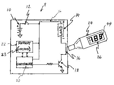
Figure 1 is a view of a generic device, having an apparatus for
identifying an electrical device, and a passive probe, according to the
present invention;
Figure 2 is a view of the circuit for the passive probe of Figure 1;
Figure 3a is a view of an algorithm for creating a sequence of
electromagnetic pulses in accordance with an identification code
according to the present invention;
Figure 3b is a view of an algorithm for detecting and translating the
sequence of electromagnetic pulses of Figure 3a into the identification
code; and
Figure 4 is an amplitude vs. time graph representation of the
sequence of electromagnetic pulses created by the apparatus of Figure 1.
CA 02678298 2009-09-04
-6-
DETAILED DESCRIPTION OF THE PREFERRED EMBODIMENTS
A preferred embodiment of the identification apparatus and method
according to the present invention is shown in Figures 1 to 4. As can be
seen from Figure 1, the invention comprises, in part, a device 8 having a
circuit comprising a power source 10 (e.g. battery), an on/off switch 12, an
electrical load 14, a electromagnetic field generator 16, a current varying
means 18, a controller 20 and a memory 22 with an identification code 23.
The controller 20 can be any device capable of controlling the flow of
current in the circuit from the power source 10 through the electrical load
14 and electromagnetic field generator 16, preferably by controlling the
current varying means 18. The controller 20 can include a CPU, a micro-
controller, a micro-processor, a Field Programmable Gate Array (FPGA),
a digital logic controller, or the like. By varying the flow of electrical
power
from the power source 10 through both the electrical load 14 and
electromagnetic field generator 16, in accordance with the identification
code, the controller 20 causes the electromagnetic field generator 16 to
create a sequence of timed electromagnetic pulses for detection by a
passive probe 24
In the preferred embodiment the current varying means 18 and
memory 23 are shown as being separate elements from the controller 20,
however it will be understood that in alternate embodiments the current
varying means 18 and/or the memory 22 may be combined with the
controller 20 into a single unit. What is important is that the identification
code 23 be provided to the controller 20. The probe 24 which is
preferably an inductive coil electromagnetic sensor is also shown in
Figure 1, with a display 26, which is explained in more detail below. All of
the elements are operatively connected or coupled together as explained
below.
The electrical load 14 is any electronic element that preferably
draws at least 20 to 100mA steady state current. However, as will be
appreciated by a person skilled in the art adequate results may be
CA 02678298 2009-09-04
-7-
obtained with current draws outside of this range in view of the various
factors known to affect the generation of electromagnetic fields.
Examples of electrical loads include, but are not limited to, an electrical
motor, a relay coil, a solenoid, a transformer, a coil having inductance, a
light (i.e. incandescent bulb or LED), a resistor, a heating element, a
semiconductor, a speaker, and the like.
The electromagnetic field generator 16 may be any electrical
electromagnetic field generator which is connected in series with the
electrical load 14, and can include, without limitation, a wire, metal strip,
or even a track on a printed circuit board. While Figure 1 depicts the
probe 24 as being positioned adjacent the electromagnetic field generator
16 on the ground or negative side of the electrical load 14, those skilled in
the art will understand the present invention also comprehends
positioning the probe 24 near the electromagnetic field generator at the
positive side of the electrical load 14. In other words the electromagnetic
field generator 16 connected between the electrical load 14 and the
positive side of the power source, in the example Figure 1, will also emit
the electromagnetic pulses.
Accordingly, if the normal position of the electromagnetic field
generator 16 does not permit adequate access for the probe (i.e. does not
sufficiently project an electromagnetic field) then the electromagnetic field
generator 16 may need to be re-routed intentionally to a location where
access by the probe 24 to the electromagnetic field generated by the
electromagnetic field generator 16 is possible (as is shown in Figure 1
with electromagnetic field generator 16 on the negative side of electrical
load 14). Most preferably the electromagnetic field generator 16 will
remain protected and invisible from the exterior by being behind a non-
metallic wall or covering such as plastic. In this sense access to the
probe means that the probe 24 can be put in sufficient proximity to the
electromagnetic field generator 16 to sense the electromagnetic field
emitted from the electromagnetic field generator 16 as explained in more
CA 02678298 2009-09-04
-8-
detail below. As described in more detail below, the pulsing of current
from the power source through the electrical load 14 and electromagnetic
field generator 16 will cause the electromagnetic field generator 16 to emit
an electromagnetic field suitably detectable by the probe 24.
The current varying means 18 is connected in series to the
electromagnetic field generator 16 between the negative ground
connection of the power source 10 and the electrical load 14. Preferably
the current varying means 18 is an NPN transistor. However, the current
varying means 18 can be any type of electronic switch, except electro-
mechanical switches such as relays. Another preferred electronic varying
means is an NMOS FET device. As mentioned above, the current varying
means 18 may be incorporated into the controller 20 in an alternate
embodiment. Also, while the drawing depicts the current varying means
18 being located on the ground or negative side of the electrical load 14,
those skilled in the art will understand the present invention also
comprehends positioning the current varying means 18 on the positive
side of the circuit. In other words a PNP transistor or an PMOS FET
device could be connected between the electrical load 14 and the positive
side of the power source 10. Of course other switches and/or user
controls may also exist to add additional functionality to the circuit.
However, only a basic circuit is described for purposes of the present
description. Since the method and apparatus for identifying an electrical
device of the present invention is incorporated into an existing electrical
device, it will be understood that the circuit of an actual device may need
to be more complex in order to provide functionality of the additional
features of the device.
In the preferred embodiment of the present invention, the current
varying means 18 is controlled by the controller 20, in a simple on and off
fashion, so that the current from the power source 10 can flow through the
electrical load 14 and the electromagnetic field generator 16, in a
controlled manner. What is important is that the current varying means 18
CA 02678298 2009-09-04
-9-
be adapted to suddenly change the current flow through the
electromagnetic field generator 16 and the electrical load 14, which are
connected in series. While the present invention is illustrated with the
current being suddenly turned on and off, it will be appreciated that in
other embodiments the electromagnetic pulses may be generated by
suddenly decreasing the current flow from on to a value less than on,
suddenly increasing the current flow from a value less than on to on,
suddenly increasing the current flow from on to a value more than on, etc.
The controller 20 is typically a CPU, micro-controller, micro-
processor, FPGA, digital logic controller, or the like, that would already be
present in the device 8. Such a controller 20 might be used to control
motors, solenoids, lights, speakers, or other aspects of the electronic
functioning of the device 8. As mentioned above, the current varying
means 18 may be a part of the controller 20 itself or a separate element
connected to the controller 20. The present invention is applicable to any
device where there is such a controller controlling the current through an
electrical load 14 and an electromagnetic field generator 16 in series.
The identification code 23 is preferably provided to the controller 20
via access to a memory 22, or other form of storage within the device 8,
as a binary code value. As mentioned above, the memory 22 need not be
a separate element of the device and may in fact be incorporated into the
controller 20. For simplicity, Figures 1, 2 and 4 show the identification
code 23 stored in memory 22 as the 8-bit binary code value, "10111001".
This 8-bit binary code value maps to OB9 in hexadecimal, and 185 in
decimal based numeral systems. However, the present invention
comprehends storing the identification code 23 in binary code values with
longer bit lengths if desired. See for example Figures 3a and 3b which
illustrate algorithms for handling an identification code stored as a 24-bit
binary code value. However, the present invention is not limited to any
one type of code format, as many types of codes and code sequences
can be used according to the present invention. The identification code
CA 02678298 2009-09-04
-10-
23 may represent the device's serial number, a special key, a random
identifier, a lot identifier or any other form of identifying means according
to the present invention. As shown in Figure 1, the probe 24 has a
display 26 with the expected 8-bit binary code value ("10111001"),
representing the identification code 23, being displayed as it was detected
from the electromagnetic field emitted by the electromagnetic field
generator 16 and translated into the decimal based numeral system, as
explained in more detail below.
At a predetermined point in the device's operation the controller 20
reads the N-bit code value of the identification code 23 one bit at a time
and controls the flow of current in the circuit from the power source 10
through the electrical load 14 and electromagnetic field generator 16, in
series, causing the electromagnetic field generator 16 to emit a sequence
of timed electromagnetic pulses in accordance with the N-bit code values
of the identification code 23. For example, the predetermined point may
be when the device is switched from off to on, or from on to off. The
predetermined point can also occur at one or more pre-set intervals
during the device's normal mode of operation. To prevent engaging the
electrical load 14 fully, and to generate the best electromagnetic pulses
for quick detection, the pulses are of short duration, preferably timed in
micro-seconds. In this respect, good results have been obtained with
pulses having durations in the range of 200-400 psec. According to the
present invention the sequence of electromagnetic pulses can be used to
generate a binary or other code for identification purposes.
As will be appreciated by those skilled in the art, the logic bits can
be according to one of several common time-based schemes. Good
results have been achieved when using two different time delays, such as
a 1.75 msec delay for a logic "1" bit and a 3.75 msec delay for a logic "0"
bit. Thus, the electrical load 14, such as a motor, for example, will be
turned on for 250 psec at the start of the sequence, followed by one or
more pulse groups for each bit in the sequence. Each pulse group
CA 02678298 2009-09-04
-11-
consists of either a 1.75 msec time delay and a subsequent 250 psec
pulse, or a 3.75 msec time delay and a subsequent 250 psec pulse as
appropriate.
The short pulsing of current through the electrical load 14 and
electromagnetic field generator 16 in series creates a varying
electromagnetic field due to interruption or sudden change of current flow
in the electrical load 14. According to the present invention the
electromagnetic pulses caused by the interruption or sudden change of
current flow can be detected by the passive probe 24, which includes a
simple inductive coil held in close proximity to the electromagnetic field
generator 16 having the electrical feed. In this sense as stated
previously, in close proximity means within the electromagnetic field
generated by the electromagnetic field generator 16, whereby the probe
can detect the changes in the electromagnetic field caused by the
electromagnetic pulses.
Turning to Figure 2 a passive electrical coil 30 is shown within the
probe 24. Good results have been achieved with a 6.8 mH (millihenry)
inductor wound on a ferrite bobbin 31. It will now be appreciated the
probe is a passive probe in the sense that it senses or receives the
electromagnetic field fluctuations generated around the electromagnetic
field generator 16, but it does not emit intentional radiation or power. Also
shown is a filter and clamping network 32 which includes biasing resistors
and capacitors to filter out any high frequency noise that may blur the
pulse by causing multiple edges. The filter and clamping network 32 also
preferably includes clamping diodes that clamp or limit the incoming
signal to the ground and battery positive supply voltage rails, to protect
the comparator IC inputs from being overdriven or damaged. The probe
24 can include other elements as is well known in the art, such as for
example an amplifier and a monostable multivibrator (not shown). The
comparator 40 functions to convert the small voltage spike sensed across
the coil 30 into a large voltage pulse with regulated amplitude. The output
CA 02678298 2009-09-04
-12-
of the comparator 40 would typically be open collector type, meaning that
the output voltage can be made equal to any voltage used by the
following circuitry, in this case the positive supply of the probe controller
42. The probe controller 42 can be a CPU, micro-controller, micro-
processor, FPGA, digital logic controller, or the like, as will be understood
by those skilled in the art. The comparator output is applied to an
interrupt type input of the probe controller 42, such that any positive-going
transition of an input pulse will interrupt a program flow within the probe
controller 42 to signal that an important timing event has occurred. The
probe controller 42 then measures the time delays between consecutive
pulses, and reconstructs the original binary code value of the identification
code 23 stored in the memory 22 of the device 8, by correlating the
measured time intervals to the logic "1" and logic "0" bits. The probe
controller 42 can then further convert the binary code value representing
the identification code 23 into the decimal based numeral system and
cause the decimal identification number 44 to appear on an integral
screen display 26, as shown in Figure 1, in a manner well known in the
art. However, it will be appreciated that the identification code 23 can be
displayed on the integral screen display 26 in any form, including using
graphic, symbolic, alphabetic, numeric, alpha-numeric, or other characters
correlated to the binary code value of the identification code 23 originally
stored in the memory 22 of the device 8. It is also contemplated that the
identification code 23 detected by the probe 24 can be stored in a
memory unit in the probe (not shown) for later retrieval, or transmitted to
another device wirelessly or wiredly (e.g. via USB cable, etc.) by known
means. Completing the probe 24 circuit is an on/off switch 46 and a
probe power source 48. It will be further appreciated that even though the
probe 24 and all of its elements has been described as a portable device,
some or all of its elements may also be housed in a non-portable
instrument case.
While Figure 1 shows an 8 bit (i.e. 1 byte) binary code value
CA 02678298 2009-09-04
-13-
representing the identification code 23 being stored in memory 22, in
accordance with another embodiment of the present invention, Figures 3a
and 3b illustrate program logic or algorithms for detecting a 24-bit binary
code value (i.e. 3 bytes, with each byte containing 8 bits).
In particular, Figure 3a depicts an algorithm for emitting
electromagnetic pulses in accordance with a 24-bit binary code value
representing the identification code 23 stored in memory 22 on the device
8. It will be understood that while reasonable results have been achieved
with this algorithm, other algorithms are comprehended by the present
invention provided that they generate a sequence of timed
electromagnetic pulses in accordance with the identification code 23
contained in the memory 22 of the device 8.
As shown, the first step is to have the memory pointer
(MEM_POINTER) set up to point to the first I.D. Byte address (I.D. BYTE
#1). Then the I.D. BYTE COUNT and BIT_COUNT counters are
initialized to three and eight, respectively, in this example since the
identification code 23 is stored as a 24-bit binary code value consisting of
3 bytes, with each byte containing 8 bits. The variable
"I.D._BYTE_OOUNT" can be any number from 1 to 64, for example, to
achieve corresponding binary code values having lengths of 8 to 512 bits
respectively. Then the first I.D. BYTE is read from memory. Then the first
I.D. BYTE is shifted left by one bit into the CARRY FLAG. Then the
power is enabled to the electrical load. Then a delay of 250 psec is
provided, after which the power to the electrical load is disabled. The next
step is to see if the bit in the CARRY FLAG is equal to 1 for example. If
yes, then a delay of 1.75 msec is incurred. If no, then the bit in the
CARRY FLAG must be a 0 and a delay of 3.75 msec is incurred. In the
next step the BIT_COUNT is reduced by 1, and a check is performed to
see if there is another bit in the first I.D. BYTE, by checking whether the
BIT_COUNT is equal to 0. If the BIT_COUNT is not equal to 0, there is
another bit in the sequence and the algorithm requires going back to get
CA 02678298 2009-09-04
-14-
the next bit value and repeating the above steps. If all of the bits in the
first I.D. BYTE have been read, then BIT_COUNT will be 0, and the
algorithm will increment the memory pointer to the next I.D. BYTE
address, and decrease the I.D. BYTE COUNT by 1. The process will then
repeat for the next byte. Once all three bytes of the I.D. BYTE have been
read, the I.D. BYTE COUNT will be 0, and the program will finish.
The short pulsing of the electrical load 14, such as a motor for
example, creates voltage spikes across the probe coil 30 due to the
interruption of current or the sudden change in current flow through the
electrical load 14. Figure 4 shows a series of voltage spikes 49 on a
graph of amplitude vs. time as they would appear at the input to
comparator 40. Although the present invention only makes use of the
positive voltage spikes, it is quite feasible to also make use of the
negative voltage spikes that have been suppressed by the clamping diode
in this preferred embodiment. As shown, the voltage spikes last about 250
psec which is the duration of time the electrical load 14 is turned on. The
interval between 3 and 5 represents 2 msec and has a logic bit value of
"1". Then the gap between 5 and 9 has a time value of 4 msec and
represents a logic bit value of "0". The voltage spikes 49 are timed, as
shown by the graph at 51 to represent a binary code value of "10111001",
which is the binary code value stored in the memory 22 of the device 8 for
the first byte. Other bit values will be stored for the other two bytes of the
three byte (24-bit) binary code value representing the identification code
23 in the present example.
Figure 3b provides a preferred algorithm for use in the probe's
controller 42. While this is a preferred algorithm it will be appreciated that
other algorithms will also provide adequate results and are comprehended
by the present invention. The algorithm of Figure 3b shows how the
voltage spikes 49 are timed and transformed back to the original three I.D.
bytes that were emitted as electromagnetic pulses using the algorithm
illustrated in Figure 3a. The probe algorithm is based on an interrupt
CA 02678298 2009-09-04
-15-
service routine (known to those skilled in the art as an "ISR"). This ISR is
triggered every time a voltage spike leading or rising edge is applied to
the external interrupt port of the probe controller 42. An internal timer
named TIMER-1 is used to measure the time delays between
consecutive voltage spikes that trigger the external interrupt port. The
initial pulse will cause the interrupt routine to turn on TIMER-1 in a reset
state, and initialize the BIT_COUNT and I.D. BYTE COUNT counters to
eight and three respectively for this example, as well as set up the
memory pointer (MEM_POINTER) to point to the first I.D. BYTE address
(I.D. BYTE#1). Each subsequent pulse causes the TIMER-1 time delay
value to be read and stored temporarily into the variable TEMP, followed
by a reset of TIMER-11 to start timing the next time delay in sequence.
The TEMP value represents the time delay measured between the last
two voltage spike interrupt pulses, and is tested to verify that the value is
within the expected range. If the TEMP value is outside of the expected
range, the algorithm is aborted with the TIMER_1 disabled. The algorithm
ensures that the measured time delays are within at least 10% of the
expected intervals for a logic "1" (1.75.0 msec +/- 0.2 msec) or a logic "0"
(3.75 msec +/- 0.4 msec) encoded input. Once a time delay has been
identified as representing either a logic "'I", or a logic "0" bit, the SET
CARRY BIT, or the CLEAR CARRY BIT, in the controller's arithmetic
logic unit (ALU), is shifted into the final answer location, that being the
detected I.D. BYTE in sequence. Once all three I.D. BYTEs have been
successfully detected, a DONE FLAG is set prior to exiting the ISR. This
action indicates to the mainline program in the probe controller 42 that the
received binary code value may be converted for display or stored as
appropriate.
The present invention further comprehends translating the detected
binary code value representing the identification code 23 into a decimal
number, and then translating each binary-coded decimal (BCD) digit in
turn to its 7-segment driver equivalent, for example, to send the complete
CA 02678298 2009-09-04
-16-
identification number 23 to a display such as a 7-segment LED type
display. The BCD numbers may also be converted to ASCII and sent to
an LCD driver chip for powering an LCD type display. However, all of the
foregoing is common knowledge to those skilled in the art, and therefore
is not described in any more detail herein.
The advantages of the present invention can now be understood.
The described invention provides a low cost way of identifying devices
that have a power source, a controller, an electrical load, and an
electromagnetic field generator. An example of such a device is a
vibrator. A vibrator may not have a surface onto which a tag or label may
be safely placed and thus the object can become unidentifiable once it is
removed from the packaging. This can create concerns for the
manufacturer if the device is brought in for a warranty claim, especially if
there is a question as to whether the product is a genuine product or a
knock off. The incremental cost for implementing the invention for each
additional device is very low, as there is nothing to be physically added to
the device. Essentially the present invention makes use of the existing
components, namely a controller 20, a memory 22, an electrical load 14
(e.g. an electric motor), and a electromagnetic field generator 16, to emit
a pulsed electromagnetic field which corresponds to the identification
code 23 of the product. The probe 24 passively determines the
identification code 23, by detecting the emitted electromagnetic pulses,
measuring the time delays between each of the pulses, and using the
time delays to derive the identification code 23 stored in the device 8.
Because the identification code 23 is imbedded in each product, in the
existing memory and/or controller parts thereof, it is essentially secret and
substantially tamper proof. In other words, for a person to be able to
tamper with the identification code of the present invention, they would
first have to know that it is encoded in the existing memory and/or
controller parts of the device. Then they would have to obtain access to
the identification code and/or firmware driving the controller, decode the
CA 02678298 2009-09-04
-17-
identification code and/or the firmware, and alter the code and/or the
firmware. These steps are considerably more difficult than removing or
obliterating an RFID tag or the like. Moreover, since the identification
code is integrated into the elements which are required to operate the
electrical device, attempting to alter or remove the identification code will
likely lead to the loss of functioning of the device. The present invention
also can be used where space limitations would prevent the use of tags or
labels and remains functional within the product even after the packaging
has been removed or lost. Further, the precise identification code 23 can
be kept secret by the manufacturer, also making the identification system
of the present invention even more tamper-proof, even assuming that
anyone can identify that an identification code is being used. The
manufacturer also has the option to base the transmission of the
identification code on a complex, rarely used, or secret set of user
interface sequences.
As can now be appreciated the present invention can be applied to
any device having a CPU, micro-controller, microprocessor, FPGA, digital
logic control, or the like which is controlling the power/current to an
electrical load and electromagnetic field generator. Examples of devices
that are suitable include kids toys such as, toy planes, cars, robots and
the like having a CPU, micro-controller, microprocessor, FPGA, or digital
logic control and motors; computers and handheld devices (the load being
a speaker for example); most household small and medium appliances
having a CPU, micro-controller, microprocessor, FPGA, or digital logic
control and a load, such as, hair dryers (the load being a heater coil or fan
motor for example), can openers (the load being a motor for example),
kettles (the load being a heater coil for example), fridges (the load being
an ice crusher motor for example), washers/dryers (the load being a light
or a motor for example), stoves (the load being a light bulb for example),
air conditioners (the load being a fan motor for example), televisions (the
load being a speaker for example), radios (the load being a speaker for
CA 02678298 2009-09-04
-18-
example), portable cassette or MP3 players (the load being a head set
speaker, or LED backlight for example), DVD players (the load being a
disk eject motor for example); motor vehicles such as
cars/buses/motorcycles/tractors (the load being a light for example);
electric or battery operated power tools (the load being a motor for
example); cell phones (the load being a vibrating motor for example);
sunglasses with built in MP3 players and ear buds (the load being a
speaker for example); tooth brushes (the load being a motor or inductive
charge coil for example); Christmas tree lights with CPU driven flash
patterns (the load being a light for example); plug in power chargers, etc.
According to another aspect of the present invention a probe can
be incorporated into one device (the primary device) that has a display,
and the identification code and electromagnetic pulse circuitry
incorporated into an associated device. The primary device could then
determine if the associated device was compatible with the primary
device, before activating a feature in the primary device. For example,
the primary device might be a rechargeable device such as a cell phone,
and the associated device could be a charging device or docking station.
Accordingly, a cell phone can be provided with a means for accepting (or
declining) charging power from a charging device/docking station, which
would be activated upon the incorporated probe identifying the charging
device as being compatible based on the identification code emitted by
the charging device/docking station.
While reference has been made in the foregoing to preferred
embodiments of the present invention it will be appreciated that variations
are possible within the broad scope of the appended claims without
departing from the scope of protection afforded thereby. Some of these
variations have been discussed above and others will be apparent to
those skilled in the art.