Note: Descriptions are shown in the official language in which they were submitted.
, - -
CA 02678330 2009-09-10
229286
QUASI-AC, PHOTOVOLTAIC MODULE FOR UNFOLDER
PHOTOVOLTAIC INVERTER
BACKGROUND
The invention relates generally to electronic power conversion and more
particularly to a quasi-AC, photovoltaic (PV) module for an unfolder PV
inverter.
Photovoltaic (PV) cells generate direct current (DC) power with the level of
DC current being dependent on solar irradiation and the level of DC voltage
inversely
dependent on temperature. When alternating current (AC) power is desired, an
inverter is used to convert the DC energy into AC energy. Typical PV inverters
employ two stages for power processing with the first stage configured for
providing a
constant DC voltage and the second stage configured for converting the
constant DC
voltage to AC current. Often, the first stage includes a boost converter, and
the
second stage includes a single-phase or three-phase inverter system. The
efficiency of
the two-stage inverter is an important parameter affecting PV system
performance and
is a product of the individual stage efficiencies.
Single phase photovoltaic inverters generally require a two-stage conversion
power circuit to convert the varying DC voltage of a PV array to the fixed
frequency
AC voltage of the grid. Traditional PV inverters use a DC link as the
intermediate
energy storage step, which means that the converter first converts the PV
array
voltage to a stable DC voltage then to a current that can be injected into the
grid.
Traditional single phase PV inverters also undesirably control the power
circuits with a fixed switching frequency using a plurality of switching
devices that
contribute to the overall switching losses. Switching losses are typically
kept as low
as possible when using traditional PV inverters by keeping the switching
frequency
low.
1
CA 02678330 2009-09-10
229286
A photovoltaic generator can include many PV modules that are connected in
series and parallel to form a solar generator. PV modules can lose their
ability to
produce power due to shading effects caused by tall objects, leaves, dust,
snow, and
so on. A photovoltaic generator delivers its maximum power by selecting a
proper
operational voltage maximum power point. Maximum power point tracking however,
works well only under optimum, non-shaded conditions. As soon as parts of a PV
module (one cell is enough) are covered by snow, dust, leaves, and the like,
the PV
generator can lose a significant portion its power.
It would be both advantageous and beneficial to provide a residential
photovoltaic (PV) energy system that is easier to install, is less expensive,
and has a
higher efficiency than that associated with traditional PV inverters. It would
be
further advantageous if the PV energy system could operate in the absence of a
DC
disconnect mechanism. It would be further advantageous if the PV energy system
could be configured to allow each PV module to operate at a corresponding
operational point that is dependent upon its shading conditions.
It would be further advantageous if modules of various powers could
effortlessly be combined in a system and if each quasi AC module were backward
compatible when presented with a DC load voltage, further making it suitable
for
three-phase systems that draw constant power.
It would be further advantageous if each quasi AC module were controllable
by using simple off the shelf unity power factor regulator ICs, ensuring
simplicity.
Additional advantages of such a PV energy system would include, without
limitation, the ability to mix different power modules in a system and also
thereby
maximize available roof area for energy generation, an efficiency gain over
the AC
module concept, no voltage on the output during installation making is safer
than
convention systems to install, provision of an array that can be mounted multi-
directional e.g. on an igloo, and mini PV cell converters in a module, each
producing
pulsing current in which various configurations are possible e.g. one
converter per 4
cells etc.
2
.n.....d=====Mraa=Nwa..
CA 02678330 2009-09-10
229286
BRIEF DESCRIPTION
Briefly, in accordance with one embodiment, a photovoltaic (PV) energy
system comprises:
a pulsating bus defined by a non-zero average value voltage that is
proportional to a rectified utility grid AC supply voltage;
at least one PV module comprising a PV generator with a converter
configured to convert a PV voltage into a pulsing current that is injected
into the
pulsing bus; and
a current unfolding circuit configured to control the polarity of AC current
injected into the utility grid in response to the injected pulsing current
such that power
generated by the at least one PV module is transferred to the utility grid.
DRAWINGS
These and other features, aspects, and advantages of the present invention
will become better understood when the following detailed description is read
with
reference to the accompanying drawings in which like characters represent like
parts
throughout the drawings, wherein:
Figure 1 illustrates a photovoltaic inverter topology that is known in the
art;
Figure 2 is illustrates a photovoltaic energy system in accordance with one
embodiment of the invention;
Figure 3 illustrates a haver-sine voltage waveform and unity power factor
current generated by a pulsed DC bus associated with a utility grid supply
according
to one embodiment of the invention;
Figure 4 is a schematic diagram illustrating a photovoltaic module integrated
with a buck topology according to one embodiment of the invention;
Figure 5 illustrates a photovoltaic buck topology including a ripple current
cancellation circuit to reduce the main buck inductor size while maintaining
ripple
specifications on a pulsed DC bus according to one embodiment of the
invention;
3
CA 02678330 2014-07-03
229286
Figure 6 illustrates the effects of shading on a string of photovoltaic
modules;
Figure 7 illustrates a portion of a photovoltaic array that is known in the
art;
Figure 8 illustrates a photovoltaic energy system in accordance with another
embodiment of the invention; and
Figure 9 illustrates an operating region for photovoltaic cells arranged into
high voltage PV modules capable of delivering a PV voltage that is always
larger in
magnitude than a peak mains grid voltage, according to one embodiment of the
invention.
While the above-identified drawing figures set forth alternative
embodiments, other embodiments of the present invention are also contemplated,
as
noted in the discussion. In all cases, this disclosure presents illustrated
embodiments
of the present invention by way of representation and not limitation. Numerous
other
modifications and embodiments can be devised by those skilled in the art which
fall
within the scope of this invention.
DETAILED DESCRIPTION
Figure 1 illustrates a photovoltaic inverter 10 topology that is known in the
art. Photovoltaic (PV) inverter 10 employs a two-stage power circuit to
convert a
varying DC voltage of a PV array 12 to a fixed frequency AC voltage for a
power grid
14. Photovoltaic inverter 10 uses a DC link capacitor 16 to implement the
intermediate energy storage step. This means the PV inverter 10 first converts
the
unstable PV DC voltage 18 to a stable DC voltage 20 that is greater than the
grid
voltage via a boost converter, and subsequently converts the stable DC voltage
20 to a
current 22 via a PWM circuit 24 that can then be injected into the grid 14.
Photovoltaic inverter 10 topology employs five switching devices 44, 46, 48,
50, 52
that are all switching at a high frequency and that undesirably contribute to
the overall
switching losses of the two-stage converter.
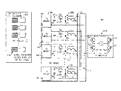
Figure 2 illustrates a photovoltaic (PV) energy system 100 in accordance
with one embodiment of the invention. PV energy system 100 employs a topology
4
CA 02678330 2009-09-10
229286
that simplifies installation, improves efficiency and reduces cost beyond that
achievable with the system topology depicted in Figure 1.
PV energy system 100 includes a pulsating bus 102 that is defined by a non-
zero average value voltage that is proportional to a rectified utility grid AC
supply
voltage and that is described in further detail below with reference to Figure
3. The
pulsating bus 102 is derived by rectification of a main utility grid supply
voltage via a
PV inverter 104 that is connected to the main utility grid; and all current
injected into
the bus 102 via the PV modules 106 is in phase with this voltage and closely
matches
the voltage waveform. The PV inverter 104 simply becomes an unfolding circuit.
The PV energy system 100 topology is particularly advantageous when the
photovoltaic cells are arranged using high voltage PV modules 106 capable of
delivering a PV voltage that is always larger in magnitude than the peak mains
grid
voltage 220 such as depicted for one embodiment in Figure 9 that illustrates a
PV
module operating region of interest 222. Each PV module 106 is configured to
operate with a corresponding bucking circuit 108 that converts the PV module
106
voltage (power) into a pulsing current that is injected into the pulsating bus
102.
Although similar to an AC module, PV module 106 together with its
corresponding bucking circuit 108 does not generate AC or DC, but instead
generates
a quasi AC. Since the PV modules 106 are configured such that they cannot
produce
energy in the absence of the voltage on the pulsating bus 102, no DC
disconnect
capability is required and the PV modules are therefore cheaper and easier to
implement. Further, the disconnect can be centrally located (inverter
¨unfolder).
Further the PV modules 106 that are each integrated with a respective
bucking circuit 108 provide a topology that requires very low power and only a
single
switching device 110. The conversion efficiency of each bucking circuit 108 is
very
high, producing very low heat. Each bucking circuit 108 employs only two
active
devices that can optionally be implemented using SiC devices that can tolerate
higher
temperature better than more conventionally used Si devices. Further, the
active
switch 110 for the buck converter 108 can be placed in the negative line of
the PV
CA 02678330 2009-09-10
229286
module 106 to simplify the gate driver and control circuit, such as depicted
in
Figure 4.
According to one aspect of the invention, a boosting circuit is not required
for the high voltage module 106 case since the working maximum power voltage
will
always be above the peak of the grid voltage when the photovoltaic cells are
arranged
into high voltage PV modules capable of delivering a PV voltage that is always
larger
in magnitude than the peak mains grid voltage.
According to one aspect of the invention, the plurality of pulsing currents
112 generated via the PV modules 106 are summed together to produce a
resultant
pulsing current on the pulsed bus 102. The resultant pulsing current is then
fed to the
PV inverter/unfolder circuit 104 that controls the AC injected into the
utility grid to
which the unfolder circuit 104 is connected. The inverter/unfolder 104 employs
a
topology that can be made very efficient (-99%), requiring virtually no
cooling and is
very inexpensive to realize.
Since each PV module is capable of operating at maximum power when
configured as illustrated in Figure 4, there is no need to design a PV array
to
accommodate a particular site. The PV energy system 100 is therefore extremely
immune to the negative effects of shading common to more conventional
topologies.
The inherent shading immunity maintains the high conversion efficiency to
harvest
more KWhrs than possible when using a conventional system.
The PV energy system 100 topology generates additional cost savings during
installation since a specialized electrician is no longer required for
installation; and a
DC disconnect is also no longer required. A DC disconnect is no longer
required
since the DC source is contained inside the PV module 106 and is not
externally
exposed.
PV modules 106 in a multiple PV module system can advantageously be
configured with different power ratings from other PV modules while retaining
interchangeability of PV modules in the absence of PV energy system
modifications
to accommodate the interchangeability of the PV modules such that the PV
energy
6
õ
CA 02678330 2009-09-10
229286
system maximizes available roof space used to attach the PV energy system.
Further,
the plurality of PV modules can be configured to provide a plurality of PV
arrays
having dissimilar directional orientations such that the PV energy system
provides
increased sun tracking capability and energy harvesting capability beyond that
achievable with a conventional PV energy system having all PV modules oriented
in
the same direction.
The PV energy system according to one embodiment is configured such that
each converter 108 and the current unfolding circuit 104 together are
configured to be
more energy conversion efficient than a conventional AC module converter. In
another embodiment, each converter and the current unfolding circuit together
are
each configured to achieve an energy conversion efficiency of about 99%.
The PV energy system according to another embodiment is configured such
that each PV module is configured to produce an output current only when the
corresponding current unfolding circuit presents a voltage to the pulsating
bus. In a
further embodiment, each PV module converter comprises at least one of a buck
converter, a boost converter, an isolated converter, or a boost converter with
flyback
capability. In yet another embodiment, each PV module converter is configured
to be
controlled via a simple and readily available off the shelf power factor
regulator IC.
In still another embodiment, each PV module is configured to deliver a PV
voltage
that is always larger in magnitude than the peak utility grid voltage. In
still another
embodiment, each PV module and the current unfolding circuit together are
configured to provide compatibility with AC energy converters to provide
energy
conversion if the pulsating bus becomes DC. In still another embodiment, each
PV
module is configured to provide constant power suitable for use with three-
phase PV
energy systems.
Figure 3 illustrates a haver-sine voltage waveform 120 and unity power
factor current 122 generated by a pulsing bus associated with a utility grid
supply
according to one embodiment of the invention.
Figure 4 is a schematic diagram illustrating a common voltage node PV
module buck topology 130 according to one embodiment of the invention.
7
CA 02678330 2009-09-10
229286
Figure 5 illustrates a PV buck topology 140 including a ripple current
cancellation circuit 142 to reduce high frequency ripple on a pulsating bus
according
to one embodiment of the invention. Ripple current cancellation circuit 142
provides
a means for reducing the main inductor 144 size without compromising the
output
ripple current requirements of the system. Ripple current cancellation circuit
142
allows use of a smaller inductor 144 having lower losses than that achievable
with a
larger inductor. Soft switching techniques can be employed to further reduce
switching losses
Looking again at Figure 2, the photovoltaic energy system 100 topology
overcomes the necessity to employ a DC link to implement an intermediate
energy
storage step such as described above with reference to Figure 1, because
bucking
circuit 108 converts the PV array 12 voltage immediately into a quasi AC
current 112.
This feature is implemented by stiffening each leg of the PV array 12 with a
large
capacitance 34, effectively shifting the DC link to the PV array 12 thereby
stabilizing
the PV array output voltage during generation of the rectified grid current.
The
subsequent inverter stage 104 merely needs to unfold the current 112 into the
grid 14,
and does so without switching losses because the inverter stage switching
devices 54,
56, 58, 60 switch only at the utility grid 14 low frequency at the zero
voltage and
current crossing points.
Each bucking circuit 108 can be seen to also include a bypass diode 114.
Each bypass diode 114 operates to protect its corresponding PV module 106
during
operating conditions when shading occurs and the PV module 106 cannot produce
the
requisite amount of energy necessary to operate the bucking circuit switching
device
110. The bypass diode 114 protects the PV module 106 during shading conditions
by
allowing the PV module current to bypass the non-functioning PV module 106 and
corresponding bucking circuit 108 without adversely impacting operating
conditions
associated with the PV modules 106 that remain unaffected by shading.
In summary explanation, a pulsating bus 102 is connected to a high voltage
PV module 106 including a buck converter 108 that generates a pulsating
current that
is injected into the bus 102 in phase with the pulsating bus voltage and
closely
8
CA 02678330 2009-09-10
229286
matches the voltage waveform. The buck converter 108 is a simple two active
device
circuit. Boosting is not required as the working maximum power voltage will
always
be above the peak of the grid voltage according to one aspect of the
invention. The
active switch for the buck converter 108 can be placed in the negative line of
the PV
module 106 to simplify the gate driver and control circuit.
Advantages provided by the PV energy system 100 include without
limitation, provision of a ripple current cancellation circuit that ensures
the buck
converter 108 inductor 144 can be made small and to ensure that high frequency
currents are sufficiently attenuated on the pulsating bus line. Further, the
PV
inverter/unfolder 104 simplifies to a simple unfolder circuit with very high
conversion
efficiency. The buck converter 108 for the PV module 106 can be realized using
SiC
devices that can tolerate higher temperatures better than Si devices, as
stated above.
Additional advantages include, without limitation, 1) the capacitor energy
storage requirements for the high voltage PV array system are significantly
reduced so
that higher reliability capacitors can be selected such as film capacitors on
the front
end of the buck converter 108; 2) ground fault detection can still be provided
in the
PV inverter/unfolder 104; and 3) if a converter capable of buck-boost
operation, or if
the buck converter 108 has a transformer as part of the converter, the PV
energy
system 100 will work with photovoltaic modules 106 whose voltage is less than
the
line voltage.
Still further advantages include, without limitation, 1) a concept that is
simpler to practice than conventional systems, 2) a higher energy harvesting
capability than possible with conventional systems, 3) reduced installation
costs as
DC wiring, requiring specially qualified electricians for installation has
been
eliminated, 4) a simplified PV array dimensioning (embedded into PV module),
and
5) a PV inverter 104 that is highly efficient and therefore significantly more
compact
and also more reliable when compared to a conventional system.
Looking now at Figure 6, the effects of shading are depicted for a string of
conventional photovoltaic modules such as depicted as PV array 12 in Figure 1.
PV
inverters have two tasks including operating the PV generator at its maximum
power
9
CA 02678330 2009-09-10
229286
point, and transforming the DC power to AC power. Maximum power point tracking
however, works well only under optimum, non-shaded conditions. As soon as
parts
of a PV module (one cell is enough) are covered by snow, dust, leaves, and the
like,
the PV generator loses a portion its power (up to 15% under certain
conditions).
When this condition occurs, a bypass diode, enumerated as 150 in Figure 7,
protects
the PV module from exposure to high reverse voltage levels that can damage the
PV
module during the shading conditions.
Figure 8 illustrates a photovoltaic energy system 200 in accordance with
another embodiment of the invention. PV energy system 200 includes a PV array
202
including a plurality of PV modules 204 connected in series in which a DC/DC
boost
converter 206 is connected across each PV module 204. Each PV module 204 can
include a single PV cell, an array of PV cells or multiple arrays of PV cells.
The PV
energy system 200 topology allows an individual operational point for every PV
module 204, ensuring that the maximum power is always achieved for the PV
array
202. If the switching transistor (e.g. MOSFET) 210 fails, the body diode 212
and the
external diodes 214 provide operating behavior as usual, such as normally
associated
with the topology illustrated in Figure 7.
The DC/DC boost converter topology described above with reference to Figure
8 can easily be employed across individual PV cells or groups of PV cells to
implement
each PV module 106 illustrated in Figure 2. The resultant architecture will
ensure that
photovoltaic cells are arranged into high voltage PV modules 106 capable of
delivering
a PV voltage that is always larger in magnitude than the peak mains grid
voltage.
In all versions of the previously described embodiments, the AC utility
voltage may not be purely sinusoidal due to the presence of harmonics. In such
cases,
the action of the unfolding circuit will not result in a haver-sine waveform
on the
pulsating bus, but rather a waveform representing the absolute value of the AC
utility
voltage.
In one case where the AC utility voltage is non-sinusoidal, the currents
injected into the bus by the PV modules may be made proportional to the
pulsating
bus voltage.
õ
CA 02678330 2009-09-10
229286
In another case where the AC utility voltage is non-sinusoidal, the currents
injected into the bus by the PV modules may be made proportional to a filtered
version of the pulsed bus voltage. This filter would reject some frequency
bands and
allow others. One example of such a filter would pass DC and the frequency
equal to
twice the line frequencies, and optionally a finite number of harmonics
thereof.
In one case where the AC utility voltage is non-sinusoidal, the currents
injected into the bus by the PV modules may be made proportional to the
absolute
value of a filtered version of the AC utility voltage. In this case, the
filter may be
constructed to band-limit the signal, including the ability to reject DC. The
filter may
be constructed to allow only signals at the fundamental of the AC line. In any
case,
the filter may also be constructed such that the fundamental component of the
current
waveform injected into the utility grid by the unfolding circuit is
proportional to the
fundamental component of the AC utility grid voltage waveform.
The above can also be accomplished by unfolding a signal-level
representation of the pulsed bus voltage such that the PV module itself can
generate a
copy of the utility voltage waveform from the bus voltage. This may then be
filtered
in the above manner. The advantage of this is that modules can now be self-
contained
without requiring a direct sample of the utility voltage. Note that when one
unfolds
the bus voltage, a phase error of 180 degrees with respect to the AC line is
possible,
assuming the actual line reference is not available. However, if the DC
component of
this representation approaches zero, as is typically the case for a utility
voltage, or if
any such DC component is removed with a filter, this phase shift is
permissible, as
once the absolute value of the filtered signal is taken, the 180 degree phase
error is
immaterial.
The advantage of using the filtering technique above is that one can improve
the stability of the system, by allowing a response only to desired AC line
voltage
frequency component. This limits the chance for instability due to arbitrary
loads.
A further advantage of using the filtering technique above is that one can
improve the safety of the system, by allowing a response only to the
fundamental
frequency of the AC line voltage frequency component. Then, when the utility
AC
11
CA 02678330 2014-07-03
229286
,
line voltage is absent, the converter produces no output to provide, for
example, anti-
islanding capability.
While only certain features of the invention have been illustrated and
described herein, many modifications and changes will occur to those skilled
in the
art. It is, therefore, to be understood that the appended claims are intended
to cover
all such modifications and changes as fall within the scope of the invention.
12