Note: Descriptions are shown in the official language in which they were submitted.
CA 02679816 2009-09-22
HIGH PRESSURE DISCHARGE LAMP LIGHTING DEVICE AND LUMINAIRE
USING SAME
Field of the Invention
The present invention relates to a high pressure
discharge lamp lighting device and a luminaire using the
same.
Background of the Invention
Although a high pressure discharge lamp is widely used
as a lamp with high luminance and high light output, a
lighting device called a stabilizer, which is a kind of
discharge lamp, is required for stable lighting. The
lighting device mainly includes a copper-iron type
consisting of an inductance and an electronic type using the
switching control of an electronic circuit. In recent years,
the electronic type has been increasingly speeded in view of
power saving.
(Conventional Example 1)
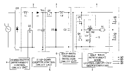
Fig. 48 shows an example of a high pressure discharge
lamp lighting device of an electronic type. This high
pressure discharge lamp lighting device includes a rectifier
DB connected to a commercial AC power source 1 for
rectifying an AC voltage thereof; a DC power source circuit
-1-
CA 02679816 2009-09-22
2 for receiving the voltage rectified by the rectifier DB as
an input and outputting a DC voltage Vdc; an inverter
circuit 4 for converting the DC voltage Vdc into a square
wave AC voltage and applying it to a high pressure discharge
lamp DL; a starting circuit 5 for generating a high voltage
to start and restart the high pressure discharge lamp DL; a
detection circuit unit 6 for detecting a state of the high
pressure discharge lamp DL; a control circuit 7 for
controlling switching elements Q3 to Q6 of the inverter
circuit 4; and a control circuit 9 for controlling the
switching element Ql of the DC power source circuit 2.
The detection circuit unit 6 is provided with a
detection circuit 6a for detecting; a voltage applied to
both ends of the high pressure discharge lamp DL and a half-
wave discharge detection unit 6b for receiving an output of
the detection circuit 6a and detecting the presence or
absence of a half-wave discharge state.
The control circuit 7 is provided with a lighting
decision unit 7a for deciding between lighting and
unlighting of the high pressure discharge lamp DL based on a
detection result of the detection circuit unit 6; a switch
circuit 7b for receiving a lighting decision signal of the
lighting decision unit 7a and switching the operation of the
inverter circuit 4 to a first operating state for generating
a high voltage for the startup of the high pressure
discharge lamp DL and a second operating state for stably
-2-
CA 02679816 2009-09-22
lighting the high pressure discharge lamp DL, and an
arithmetic circuit 7c for receiving the detection result of
the detection circuit unit 6 to determine the chopping
frequency and ON period of the switching elements Q5 and Q6.
An output of the arithmetic circuit 7c passes through the
switch circuit 7b and then controls each of the switching
elements Q3 to Q6 during the second operating state.
The control circuit 9 is provided with a Vdc detection
circuit 9a for detecting an output voltage Vdc of the DC
power source circuit 2; and a Q1 control circuit 9b for
controlling the switching element Ql based on a detection
result of the Vdc detection circuit 9a.
Fig. 49 shows the waveforms of the respective parts of
the high pressure discharge lamp lighting device of Fig. 48.
An operation from the inputting of a commercial AC power 1
to the stable lighting of the high pressure discharge lamp
DL is shown therein, and the AC voltage Vs of the commercial
AC power source 1, the output voltage Vdc of a step-up
chopper circuit serving as the DC power source circuit 2,
the both-end voltage Vo of the high pressure discharge lamp,
e.g., high-intensity discharge lamp (HID lamp) DL; the lamp
current Io, the output of the lighting decision unit 7a, and
the operating states of the switching elements Q3 to Q6 are
shown from the top.
When a commercial AC power source 1 is input, the DC
power source circuit 2 keeps the DC voltage Vdc constant at
-3-
CA 02679816 2009-09-22
a predetermined value both during unlighted state of the
high pressure discharge lamp DL is not lighted and during
lighted state of the high pressure discharge lamp DL is
lighted by allowing the control circuit 9 to turn the
switching element Ql on and off at several 10 kHz and
properly control the pulse width depending on the DC voltage
Vdc. Also, the DC power source circuit 2 functions to
improve the input power factor from the commercial AC power
source 1 and suppress input current distortion.
When the DC voltage Vdc reaches a predetermined value,
the inverter circuit 4 starts operation thereof. At this
period of time, the high pressure discharge lamp DL is in an
unlighted state, which is equivalent to an open state, and
thus the high pressure discharge lamp DL is in a high
impedance state whose equivalent impedance is close to
infinity. At this time, the inverter circuit 4 starts
operation thereof in the first operating state for starting
the high pressure discharge lamp DL, and the ON state of the
switching elements Q3 and Q6 and the ON state of the
switching elements Q4 and Q5 are alternately repeated at a
predetermined frequency f0 (about several 100 kHz).
The frequency f0 is a frequency which is close to a
resonance frequency fr of a serial resonance circuit
including a primary coil Nl of a pulse transformer L3 and a
capacitor C3, wherein a high voltage of sine wave is
generated in the primary coil N1. The high voltage of sine
-4-
CA 02679816 2009-09-22
wave generated in the primary coil N1 is stepped up by the
winding ratio between the primary coil N1 and secondary coil
N2 of the pulse transformer L3, and applied to the high
pressure discharge lamp DL through a capacitor C2. As a
result, the high pressure discharge lamp DL dielectrically
breaks down and is started up.
When the high pressure discharge lamp DL is started up,
the high pressure discharge lamp DL becomes a low impedance
state close to a short circuit, and the both-end voltage Vo
of the high pressure discharge lamp DL is reduced to
approximately 0 V. If the both-end voltage Vo of the high
pressure discharge lamp DL is below a threshold value of a
lighting decision voltage, the lighting decision unit 7a
decides that the high pressure discharge lamp DL is lighted,
and then an output signal of the lighting decision unit 7a
changes from H level to L level and is input to the switch
circuit 7b of the control circuit 7. The switch circuit 7b
receives this signal and switches the operation of the
inverter circuit 4 to the second operating state for stably
lighting the high pressure discharge lamp DL.
During the second operating state of the inverter
circuit 4, the switching elements Q3 and Q4 are alternately
turned on and off at a predetermined frequency fa (about
several hundreds of Hz). At this time, the switching
elements Q5 and Q6 repeat an operation in which the
switching element Q6 is turned on and off at a predetermined
-5-
CA 02679816 2009-09-22
frequency fb (about several tens of kHz) during an ON period
of the switching element Q3 and the switching element Q5 is
turned on and off at the predetermined frequency fb (about
several tens of kHz) during an ON period of the switching
element Q4. By this polarity inverting type step-down
chopper operation, the square wave AC voltage of the
frequency fa is applied to the high pressure discharge lamp
DL. At this time, the capacitor C2 and an inductor L2
function as a filter circuit of a step-down chopper circuit,
and reverse parallel diodes incorporated in the switching
elements Q5 and Q6 function as regenerative current carrying
diodes of the step-down chopper circuit.
The both-end voltage of the high pressure discharge
lamp DL is low right after the startup of the lamp, and
increased as the voltage and temperature in the lamp become
higher, and then the high pressure discharge lamp DL is
becomes a stable lighting state when a rate value is reached.
The control circuit 7 detects a state of the high
pressure discharge lamp DL by the detection circuit 6a, and
properly controls the chopping frequency or ON period of the
switching elements Q5 and Q6 by the arithmetic circuit 7C
based on the both-end voltage of the high pressure discharge
lamp DL so that an appropriate power is supplied to the high
pressure discharge lamp DL and the high pressure discharge
lamp DL is stably lighted.
In the conventional example, in a startup process, a
-6-
CA 02679816 2009-09-22
half-wave discharge detecting function is stopped in order
to prevent error detection. Thus, the detecting operation
is started after the high pressure discharge lamp DL is
shifted to a stable lighting state. If a half-wave
discharge is detected, it is determined that an end stage of
the life span of the high pressure discharge lamp DL has
come, and thus the discharge lamp DL is_shifted to a
protecting operation for stopping or reducing the output of
the lighting device.
(Conventional Example 2)
Fig. 50 shows an example of another high pressure
discharge lamp lighting device. This lighting device
includes a rectifier DB connected to a commercial AC power
source 1 for rectifying an AC voltage thereof; a DC power
source circuit 2 for receiving the voltage rectified by the
rectifier DB as an input and outputting a DC voltage Vdc; a
step-down chopper circuit 3 controlled to supply an
appropriate power to the high pressure discharge lamp DL by
using the DC voltage Vdc as a power source; an inverter
circuit 4 for converting the DC output of the step-down
chopper circuit 3 into a square wave AC voltage and applying
it to the high pressure discharge lamp DL; and a starting
pulse generating circuit for generating and applying a high
voltage required for starting up the high pressure discharge
lamp DL, and a control circuit for controlling the above
components to operate properly.
-7-
CA 02679816 2009-09-22
Details of the configuration of the starting pulse
generating circuit will be described. The starting pulse
generating circuit is provided with a pulse transformer PT
whose secondary coil N2 is connected between an output of
the inverter circuit 4 and the high pressure discharge lamp
DL; a voltage response type switching element Q7 which is ON
when the both-end voltage exceeds a predetermined value; a
capacitor C7 connected in series between a primary coil N1
of the pulse transformer PT and the switching element Q7;
and a resistor R7 connected in parallel to the switching
element Q7 for controlling current for charging the
capacitor Q7 when the switching element Q7 is off.
The configuration of the control circuit will be
described. A half-wave discharge detection circuit unit 6,
a lighting decision unit 7a, and a power factor improvement
control circuit unit 9 may have the same configuration as
Fig. 48. A step-down chopper output detection unit 7d
detects an output voltage of the step-down chopper circuit 3,
and a step-down chopper control circuit unit 8 controls the
switching element Q2 to have a predetermined current
depending on the output voltage of the step-down chopper
circuit 3, to supply an appropriate power to the high
pressure discharge lamp DL. A polarity inversion control
circuit 7e performs switching control of the switching
elements Q3 to Q6 of the inverter circuit 4.
Hereinafter, the operation of this circuit will be
-8-
CA 02679816 2009-09-22
described with reference to the waveform diagram of Fig. 51.
During unlighting of the high pressure discharge lamp DL,
the step-down chopper circuit 3 outputs a DC voltage higher
than the voltage of the high pressure discharge lamp DL
during stable lighting to smoothly start up the high
pressure discharge lamp DL, converts it into a square wave
AC voltage by the inverter circuit 4, and applies it to the
high pressure discharge lamp DL through the starting pulse
generating circuit.
In the starting pulse generating circuit, the
capacitor C7 is charged through the primary coil Nl of the
pulse transformer PT and the resistor R7. Here, the sum of
the output voltage of the inverter circuit 4 and a voltage
Vc7 of the capacitor C7 is applied to the switching element
Q7 of voltage response type. Meanwhile, if a value of the
output voltage of the inverter circuit 4 is almost equal to
a value of the output voltage of the step-down chopper
circuit 3 and the output voltage of the step-down chopper
circuit 3 is set to Vc2, when the square wave is stable, a
voltage of jVc2j-jVc7j is provided, thus failing to reach an
on voltage of the switching element Q7 and turn on the
switching element Q7. However, if the polarity of the
square wave voltage is inverted, the voltage of the
capacitor C7 does not change rapidly because the resistor R7
is connected thereto, and a voltage of jVc2j+jVc7j is
applied to the switching element Q7, thereby reaching the ON
-9-
CA 02679816 2009-09-22
voltage of the switching element Q7 and turning on the
switching element Q7.
Thus, a steep pulse current flows in the primary coil
N1 of the pulse transformer Nl, and a high voltage, which is
a multiple of the voltage generated in the primary coil N1
by the winding ratio, is generated in the secondary coil N2
and applied to the high pressure discharge lamp DL by using
the capacitor C2 connected to the output of the step-down
chopper circuit 3 and the capacitor C7 of the starting pulse
generating circuit as a power source, thereby dielectrically
breaking down the high pressure discharge lamp DL.
When the high pressure discharge lamp DL is started up,
the startup of the high pressure discharge lamp DL is
detected by the lighting decision unit 7a, the output
voltage of the step-down chopper circuit 3 is detected by
the step-down chopper output detection unit 7d, the
switching element Q2 is controlled to have a predetermined
current depending on the output voltage by the step-down
chopper control circuit unit 8, and an appropriate power
having a rectangular waveform is supplied to the high
pressure discharge lamp DL through the inverter circuit 4,
thus stably lighting up the high pressure discharge lamp DL.
It is known that the high pressure discharge lamp DL
is in a so-called `half-wave discharge' state, which is one
of abnormal conditions of the end stage of the life span, in
which discharge is asymmetric as discharge is formed from
-10-
CA 02679816 2009-09-22
one electrode only or discharge from one electrode is
suppressed. In case of `half-wave discharge', a normal
lighting control cannot be performed, and thus there is a
risk of abnormal heating of the high pressure discharge lamp
lighting device or an increase of electrical stress on the
electronic parts constituting the high pressure discharge
lamp lighting device. Therefore, there is provided a high
pressure discharge lamp lighting device which has the half-
wave discharge detection circuit unit 6 installed therein
and has a protection function for stopping an operation of a
ballast when detecting a half-wave discharge of the high
pressure discharge lamp DL.
Fig. 52 shows an operating diagram of a protection
function by detection of a half-wave discharge in the high
pressure discharge lamp lighting device of Fig. 50. A half-
wave discharge phenomenon is detected by detecting
variations of the output voltage of the step-down chopper
circuit 3 by the half-wave discharge detection circuit unit
6 of Fig. 50. If a half-wave discharge is detected, power
supply to the high pressure discharge lamp DL is stopped by
stopping a control signal from the step-down chopper control
circuit unit 8 to the switching element Q2.
In the conventional example, in a startup process, a
half-wave discharge detecting function is stopped in order
to prevent error detection. Thus, the detecting operation
is started after the high pressure discharge lamp DL is
-11-
CA 02679816 2009-09-22
shifted to a stable lighting state. If a half-wave
discharge is detected, the discharge lamp DL is shifted to a
protecting operation for stopping or reducing the output of
the lighting device.
(Conventional Example 3)
Fig. 54 is a circuit diagram of a high pressure
discharge lamp lighting device disclosed Japanese Patent
Laid-open Application No. 2005-100829. To a DC power source
circuit 2, a serial circuit of capacitors Cel and Ce2 and a
serial circuit of switching elements Q5 and Q6 are connected
in parallel. A serial circuit of an inductor L2 and a
capacitor C2 is connected between a connection point of the
capacitors Cel and Ce2 and a connection point of the
switching elements Q5 and Q6. A high pressure discharge
lamp DL is connected to both ends of the capacitor C2
through a secondary coil of a pulse transformer PT of a
starting circuit S. The switching elements Q5 and Q6 are
composed of MOSFETs, and includes reverse parallel diodes
therein. An auxiliary chopper circuit 9 consisting of a
diode D9, a switching element Q9, and an inductor L9 is
additionally provided.
Fig. 55 shows operation waveforms of the respective
parts from an unlighted state to a lighted state. A control
signal applied to the switching elements Q5, Q6, and Q9 has
the operation waveforms shown in Fig. 55.
The on and off of the switching elements Q5 and Q6 is
-12-
CA 02679816 2009-09-22
controlled through a driving circuit 72 by a control signal
output from a control circuit 71. During stable lighting,
in a first period Ti, the switching element Q5 is turned on
and off at a high frequency, and thus the switching element
Q6 is turned off. In a second period T2, the switching
element Q6 is turned on and off at a high frequency, and
thus the switching element Q5 is turned off. The capacitors
Cel and Ce2 have sufficiently large capacitance, and the
voltage Vcel of the capacitor Cel and the voltage Vce2 of
the capacitor Ce2 are not varied in an alternating period of
the periods Ti and T2. The voltage Vdc of the DC power
source circuit 2 is divided by the capacitors Cel and Ce2,
and thus Vdc=Vcel+Vce2. If the capacitances of the
capacitors Cel and Ce2 are almost the same, Vicel -Vice2.
In the first period T1, when the switching element Q5
is turned on, current flows in the order of capacitor Cel,
switching element Q5, inductor L2, capacitor C2 (starting
circuit 5 and high pressure discharge lamp DL) and capacitor
Cel. When the switching element Q5 is turned off, current
flows in the order of inductor L2, capacitor C2 (starting
circuit 5 and high pressure discharge lamp DL), capacitor
Ce2, switching element Q6 (reverse parallel diode thereof)
and inductor L2 by energy stored in the inductor L2.
In the second period T2, when the switching element Q6
is turned on, current flows in the order of capacitor Ce2,
capacitor C2 (high pressure discharge lamp DL and starting
-13-
CA 02679816 2009-09-22
circuit 5), inductor L2, switching element Q6 and capacitor
Ce2. When the switching element Q6 is turned off, current
flows in the order of inductor L2, switching element Q6
(reverse parallel diode thereof), capacitor Ce, capacitor C2
(high pressure discharge lamp DL and starting circuit 5) and
inductor L2 by energy stored in the inductor L2. Therefore,
during stable lighting, the voltage Vo of the high pressure
discharge lamp DL becomes a square wave voltage having a low
frequency shown on the right side (the periods Tl and T2
following the period T3) of Fig. 55.
During unlighted state of the high pressure discharge
lamp DL, the starting circuit 5 generates a high pulse
voltage for startup. An operation waveform during unlighted
state during which the starting circuit 5 operates is shown
on the left side (prior to the period T3) of Fig. 55.
During unlighted state of the high pressure discharge lamp
DL, the amplitude of the lamp voltage Vo is Vdc/2, to which
a high pulse voltage is superposed, thereby reaching a peak
voltage Vp.
In accordance with the third conventional example,
during unlighted state and in a time period from the startup
of the high pressure discharge lamp DL to a definite
transition to arc discharge, only the switching element Q5
is turned on and off at a high frequency, and the switching
element Q6 is kept off, thereby preventing a half-wave
discharge by performing a DC startup (DC voltage input) . If
-14-
CA 02679816 2009-09-22
a half-wave discharge occurs when there is a transition from
an unlighted state to a lighted state, current flows only
in one direction in the discharge lamp DL. However, if only
the switching element Q5 is turned on and off, current
flowing only in one direction due to occurrence of half-wave
discharge can be prevented, even though the discharge lamp
DL may not be turned on.
As shown in the waveform of the lamp voltage Vo of Fig.
55, in a period from the startup of the lamp DL to a
definite transition to arc discharge, the period T3 for
several tens of seconds to several minutes is set, during
which only the switching element Q5 is continuously turned
on and off during unlighted state to thus stabilize the
discharge, and thereafter the switching element Q6 is also
turned on and off so as to be switched alternately with the
switching element Q5.
In the period T3 for stabilizing the discharge, while
the switching element Q5 is on, current Il flows in the high
pressure discharge lamp DL (and the capacitor C2) through
the inductor L2 so that energy is stored in the inductor L2.
When the switching element Q5 is off, the energy stored in
the inductor L2 is emitted and current Il' flows in the high
pressure discharge lamp DL (and the capacitor C2) through
the capacitor Ce2, a reverse parallel diode of the switching
element Q6, and the inductor L2. At this time, the energy
emitted from the capacitor Cel is applied to the capacitor
-15-
CA 02679816 2009-09-22
Ce2.
However, only the switching element Q5 is driven in
the period T3 so that there is no path for emitting the
energy stored in the capacitor Ce2 when a DC startup is
carried out, thus only leading to the storage of a voltage
in the capacitor Ce2. Consequently, an auxiliary chopper
circuit 9 indicated in dotted line is installed in the
circuit of Fig. 54 to provide an emission path of the energy
to be charged in the capacitor Ce2.
By adding the auxiliary chopper circuit 9 shown in Fig.
54, if a voltage stored in the capacitor Ce2 exceeds a
predetermined value, the switching element Q9 is turned on,
and the energy charged in the capacitor Ce2 is discharged
and stored in the inductor L9 through the switching element
Q9. Next, when the switching element Q9 is turned off, the
energy stored in the inductor L9 is emitted and charged in
the capacitor Cel through the diode D9. At this time, the
switching element Q9 is turned on and off at a high
frequency. As a result, the energy stored in the capacitor
Ce2 can be emitted, and an overvoltage application can be
prevented.
It is known that a`half-wave discharge' phenomenon
occurs not only in the above-mentioned end stage of the
lifespan, but also during the startup of the high pressure
discharge lamp DL. Figs. 53A to 53C show waveforms
illustrating `half-wave discharge' occurring during startup,
-16-
CA 02679816 2009-09-22
in which Fig. 53A shows a waveform illustrating one example
of `half-wave discharge' during startup in the first
conventional example (the circuit of Fig. 48), Figs. 53B and
53C show waveforms illustrating one example of `half-wave
discharge' during startup in the second conventional example
(the circuit of Fig. 50), Figs. 53A and 53B represent
transition to discharge to a typical full wave after the
duration of the half-wave discharge, and Fig. 53C represents
a continuing half-wave discharge.
`Half-wave discharge' arises because the cathode
electrode from which electrons are emitted towards anode
electrode cannot transit from glow discharge to arc
discharge, and is caused by instability of thermal electron
emission from the cathode electrode. The causes thereof may
be low electrode temperature, adhesion of impurities, or the
like.
`Half-wave discharge' during startup is a phenomenon
which occurs during a process leading to normal lighting as
shown in Figs. 53A and 53B. Thus, if the protection
function for stopping the operation of a ballast by
detection by the aforementioned half-wave discharge
detection circuit unit 6 is operated, there occurs a failure
that the high pressure discharge lamp DL is not lighted.
Therefore, the aforementioned function of protection is
stopped for a predetermined time period from the startup of
the high pressure discharge lamp DL.
-17-
CA 02679816 2009-09-22
Japanese Patent Laid-open Application No. 2005-100829
discloses the high pressure discharge lamp lighting device
as shown in Figs. 54 and 55, and also discloses a technique
in which half-wave discharge is prevented by controlling the
switching elements such that a DC voltage is applied in the
period T3 from the startup of the high pressure discharge
lamp DL to a secure transition to arc discharge, but the
number of parts increases because of the addition of the
auxiliary chopper circuit 9. Further, once a DC voltage is
applied and there is a definite transition to arch discharge,
the temperature of the arc tube of the high pressure
discharge lamp increases and electrons are easily emitted
from both of the electrodes, thus making transition to
stable lighting easier. However, under a condition in which
a DC voltage is applied, one electrode is fixed as an anode
and the opposite electrode is fixed as a cathode, and thus a
difference is easily generated between the states of both
electrodes depending on the duration of the DC voltage.
Moreover, a DC voltage application time for securely
suppressing the occurrence of half-wave discharge is varied
depending on the type or state of the high pressure
discharge lamp, so it is very difficult to properly set the
DC voltage application time.
Additionally, if `half-wave discharge' continues, a
difference is generated between the states of both
electrodes and it is difficult to make a transition to
-18-
CA 02679816 2009-09-22
stable discharge of a full wave. Further, a vapor pressure
inside the arc tube of the high pressure discharge lamp
increases due to arc discharge at one side, and it is also
difficult to maintain `half-wave discharge'. Although the
high pressure discharge lamp returns to the unlighted state
because extinguishing occurs, the inside of the arc tube has
a high temperature and high pressure. Thus, it is necessary
to wait until the lowering of the temperature and pressure
in the arc tube to enter a so-called restart mode and start
up the high pressure discharge lamp again and it takes time
to start up the high pressure discharge lamp.
Summary of the Invention
In view of the above, the present invention provides a
high pressure discharge lamp lighting device which can
quickly shift to an appropriate discharge of a full wave in
the event of a half-wave discharge during startup of a high
pressure discharge lamp.
In accordance with a first aspect of the present
invention, there is provided a high pressure discharge lamp
lighting device, including: a DC power source circuit; a
power supply circuit for converting an output from the DC
power source circuit into a square wave AC output to be
supplied to a high pressure discharge lamp; a starting
circuit for applying a high voltage output for lamp startup
-19-
CA 02679816 2009-09-22
to the high pressure discharge lamp; a control circuit for
controlling the DC power source circuit, the power supply
circuit and the starting circuit; and a half-wave discharge
detection circuit for detecting a half-wave discharge in
which load voltages or load currents of two half periods of
two different polarities of the square wave AC output are
asymmetric with each other. The half-wave discharge
detection circuit detects the half-wave discharge at an
initial stage of the lamp startup from dielectric breakdown
of the high pressure discharge lamp until a lamp voltage of
the high pressure discharge lamp approximates a rated lamp
voltage, and judges that the half-wave discharge has
occurred, if it is detected that the absolute value of a
load voltage difference or a load current difference of the
two different polarities is larger than a maximum variation
of a load voltage difference or a load current difference of
the two different polarities of the square wave AC output
during normal lighting of the discharge lamp. Further, the
control circuit adjusts the output of each of at least one
of the DC power source circuit, the power supply circuit,
and the starting circuit if the half-wave discharge
detection circuit detects the half-wave discharge, thereby
controlling the magnitude of a voltage of a square wave half
period of one polarity having a load voltage of a larger
magnitude and that of a square wave half period of the other
polarity having a load voltage of a smaller magnitude to
-20-
CA 02679816 2009-09-22
approximate to each other.
In accordance with a second aspect of the present
invention, there is provided a high pressure discharge lamp
lighting device, including: a DC power source circuit; a
power supply circuit for converting an output from the DC
power source circuit into a square wave AC output to be
supplied to a high pressure discharge lamp; a starting
circuit for applying a high voltage output for lamp startup
to the high pressure discharge lamp; a control circuit for
controlling the DC power source circuit, the power supply
circuit and the starting circuit; and a half-wave discharge
detection circuit for detecting a half-wave discharge in
which load voltages or load currents of two half periods of
two different polarities of the square wave AC output are
asymmetric with each other. The half-wave discharge
detection circuit detects the half-wave discharge at an
initial stage of startup from dielectric breakdown of the
high pressure discharge lamp until a lamp voltage of the
high pressure discharge lamp approximates a rated lamp
voltage, and judges that a half-wave discharge condition has
occurred, if the absolute value of a load voltage difference
or a load current difference of the two different polarities
is larger than a maximum variation of a load voltage
difference or a load current difference of the two different
polarities of the square wave AC output during normal
lighting of the discharge lamp. Further, if the half-wave
-21-
CA 02679816 2009-09-22
discharge detection circuit detects the half-wave discharge,
the control circuit turns off the high pressure discharge
lamp for a predetermined time period and then restarts the
lamp, and wherein when restarting the lamp, the control
circuit adjusts the output of each of at least one of the DC
power source circuit, the power supply circuit, and the
starting circuit, thereby controlling the magnitude of a
voltage or a current of a square wave half period of one
polarity having a load voltage of a larger magnitude to
approximate to that of a square wave half period of the
other polarity having a load voltage of a smaller magnitude.
In accordance with a third aspect of the present
invention, there is provided a luminaire including one of
the high pressure discharge lamp lighting device of the
first and the second aspect of the present invention.
In accordance with the present invention, the half-
wave discharge detection circuit decides that a half-wave
discharge phenomenon has occurred, at an initial stage of
startup from dielectric breakdown of the high pressure
discharge lamp until reaching an approximate rated lamp
voltage of the high pressure discharge lamp, if it is
detected that an absolute value of a voltage difference or
current difference of the other polarity is larger than the
maximum variation of a voltage difference or current
difference of each half period of a square wave AC output
during normal lighting.
-22-
CA 02679816 2009-09-22
The control circuit controls such that a voltage value
of the square wave half period of a polarity having load
voltage of larger magnitude and a voltage value of a square
wave half period of a polarity having the load voltage of
smaller magnitude are approximate to each other by adjusting
the output of at least one of the DC power source circuit,
the power supply circuit, and the starting circuit upon
decision of a half-wave discharge by the half-wave discharge
detection circuit, thereby making a transition to an
operation of a half-wave improvement mode for facilitating a
discharge from an electrode in a cathode period, and
extinguishing the high pressure discharge lamp for a
predetermined period.
Thereafter, when restarting, it is possible to prevent
the duration of a half-wave discharge phenomenon in a
startup process because a discharge from an electrode in a
cathode period is facilitated by performing a half-wave
improvement control to make a voltage value of a square wave
half period of a polarity having the load voltage of larger
magnitude and a voltage value of a square wave half period
of a polarity having the load voltage of smaller magnitude
approximate to each other by adjusting the output of at
least one of the DC power source circuit, the power supply
circuit, and the starting circuit. As a result, it is
possible to make a quick transition to a stable lighting
mode.
-23-
CA 02679816 2009-09-22
Brief Description of the Drawings
The objects and features of the present invention will
become apparent from the following description of preferred
embodiments, given in conjunction with the accompanying
drawings, in which:
Fig. 1 is a circuit diagram of a first embodiment of
the present invention of the present invention;
Fig. 2 is an operation waveform diagram of the first
embodiment of the present invention;
Fig. 3 is a circuit diagram of a second -embodiment of
the present invention;
Fig. 4 is an operation waveform diagram of the second
embodiment of the present invention;
Fig. 5 is a circuit diagram of a third embodiment of
the present invention;
Fig. 6 is an operation waveform diagram of the third
embodiment of the present invention;
Fig. 7 is an operation waveform diagram of the third
embodiment of the present invention;
Fig. 8 is a circuit diagram of a fourth embodiment of
the present invention;
Fig. 9 is an operation waveform diagram of the fourth
embodiment of the present invention;
Fig. 10 is an operation waveform diagram of the fourth
-24-
CA 02679816 2009-09-22
embodiment of the present invention;
Fig. 11 is an operation waveform diagram of a fifth
embodiment of the present invention;
Fig. 12 is an operation waveform diagram of the fifth
embodiment of the present invention;
Fig. 13 is an operation waveform diagram of the fifth
embodiment of the present invention;
Fig. 14 is an operation waveform diagram of a sixth
embodiment of the present invention;
Fig. 15 is an operation waveform diagram of the sixth
embodiment of the present invention;
Fig. 16 is an operation waveform diagram of the sixth
embodiment of the present invention;
Fig. 17 is an operation waveform diagram of a seventh
embodiment of the present invention;
Fig. 18 is an operation waveform diagram of the
seventh embodiment of the present invention;
Fig. 19 is an operation waveform diagram of an eighth
embodiment of the present invention;
Fig. 20 is a circuit diagram of a ninth embodiment of
the present invention;
Fig. 21 is an operation waveform diagram of the ninth
embodiment of the present invention;
Fig. 22 is a circuit diagram of a modified example of
the ninth embodiment of the present invention;
Fig. 23 is an operation waveform diagram of a modified
-25-
CA 02679816 2009-09-22
example of the ninth embodiment of the present invention;
Fig. 24 is an operation waveform diagram of a tenth
embodiment of the present invention;
Fig. 25 is an operation waveform diagram of the tenth
embodiment of the present invention;
Fig. 26 is an operation waveform diagram of the tenth
embodiment of the present invention;
Fig. 27 is an operation waveform diagram of the tenth
embodiment of the present invention;
Fig. 28 is an operation waveform diagram of an
eleventh embodiment of the present invention;
Fig. 29 is an operation waveform diagram of a twelfth
embodiment of the present invention;
Fig. 30 is an operation waveform diagram of a
thirteenth embodiment of the present invention;
Fig. 31 is an operation waveform diagram of a
fourteenth embodiment of the present invention;
Fig. 32 is an operation waveform diagram of a
fifteenth embodiment of the present invention;
Fig. 33 is an operation waveform diagram of the
fifteenth embodiment of the present invention;
Fig. 34 is an operation waveform diagram of a
sixteenth embodiment of the present invention;
Fig. 35 is an operation waveform diagram of a
seventeenth embodiment of the present invention;
Fig. 36 is an operation waveform diagram of the
-26-
CA 02679816 2009-09-22
seventeenth embodiment of the present invention;
Fig. 37 is an operation waveform diagram of an
eighteenth embodiment of the present invention;
Fig. 38 is an operation waveform diagram of the
eighteenth embodiment of the present invention;
Fig. 39 is an operation waveform diagram of a
nineteenth embodiment of the present invention;
Fig. 40 is an operation waveform diagram of a
twentieth embodiment of the present invention;
Fig. 41 is an operation waveform diagram of a twenty-
first embodiment of the present invention;
Fig. 42 an operation waveform diagram of the twenty-
first embodiment of the present invention;
Fig. 43 is an operation waveform diagram of a twenty-
second embodiment of the present invention;
Fig. 44 is an operation waveform diagram of a twenty-
third embodiment of the present invention;
Fig. 45 is an operation waveform diagram of a twenty-
fourth embodiment of the present invention;
Fig. 46 is an operation waveform diagram of a twenty-
fifth embodiment of the present invention;
Figs. 47A to 47C are perspective views showing the
outer appearances of a luminaire of a twenty-sixth
embodiment of the present invention;
Fig. 48 is a circuit diagram of a first conventional
example;
-27-
- -- ------- --,.__.___-_- ---__- _------_.____ _
CA 02679816 2009-09-22
Fig. 49 is an operation waveform diagram of the first
conventional example;
Fig. 50 is a circuit diagram of a second conventional
example;
Fig. 51 is an operation waveform diagram of the second
conventional example upon startup;
Fig. 52 is an operation waveform diagram of the second
conventional example upon occurrence of half-wave discharge
after stable lighting;
Figs. 53A to 53C are operation waveform diagrams
showing a half-wave discharge right after startup in the
first and second conventional examples;
Fig. 54 is a circuit diagram of a third conventional
example; and
Fig. 55 is an operation waveform diagram of the third
conventional example;
Detailed Description of the Embodiments
Hereinafter, embodiments of the present invention will
be described in detail with reference to the accompanying
drawings which form a part hereof.
(Embodiment 1)
Fig. 1 shows a circuit diagram of a lighting device of
a first embodiment of the present invention. An AC power
source 1 is full-wave rectified by a rectifier DB, and
-28-
CA 02679816 2009-09-22
converted into a DC voltage by a DC power source circuit 2.
The DC power source circuit 2 is comprised of a step-up
chopper circuit having an inductor Ll, a switching element
Qi, a diode Dl, and a capacitor Cl. The switching element
Ql of the DC power source circuit 2 is turned on and off at
a high frequency by a power factor improvement control
circuit unit 9. The power factor improvement control
circuit unit 9 can be easily realized by using a
commercially available integrated circuit (MC33262 or the
like). Although not shown, current of the switching element
Ql, current of the inductor L1, and input and output
voltages of the DC power source circuit 2 are monitored by
the power factor improvement control circuit unit 9, an AC
input from the commercial AC power source 1
is converted into a predetermined DC voltage, and a power
factor improvement control for giving resistance to the
circuits is performed such that the phase of an input
current and the phase of an input voltage are identical to
each other.
A step-down chopper circuit 3 and an inverter circuit
4 serving as a power conversion circuit are connected to the
output of the DC power source circuit 2. The step-down
chopper circuit 3 includes a switching element Q2, a diode
D2, an inductor L2, and a capacitor C2, is a circuit that
outputs a DC voltage obtained by stepping down an input
voltage, and is used as a stabilizer that adjusts power
-29-
CA 02679816 2009-09-22
supplied to the high pressure discharge lamp DL by
controlling on and off of the switching element Q2 by a PWM
signal from a step-down chopper control circuit unit B.
The inverter circuit 4 is a full-bridge circuit
including switching elements Q3 to Q6. As the pair of the
switching elements Q3 and Q6 and the pair of the switching
elements Q4 and Q5 are alternately turned on at a low
frequency of several tens to several hundreds of Hz by a
control signal from a control circuit unit 7, the inverter
circuit 4 supplies a square wave AC power to the discharge
lamp DL. Further, upon startup, the switching elements Q3
and Q4 are alternately turned on at a high frequency of
several tens to several hundreds of kHz which is near a
resonance frequency of a resonant starting circuit 5 or a
frequency near 1 of the integer part thereof, thereby
supplying a high voltage for startup to the high pressure
discharge lamp DL.
The resonant starting circuit 5 is comprised of a
resonance step-up circuit including a pulse transformer L3
connected between one end of the high pressure discharge
lamp DL and a connection point of the switching elements Q3
and Q4; a serial circuit of a capacitor C3; and a resistor
R3 that are inserted between the center tap of the pulse
transformer L3 and the ground.
The control circuit unit 7 detects a lamp voltage Vo
and a lamp current Io of the high pressure discharge lamp DL
-30-
CA 02679816 2009-09-22
by a detection unit (not shown), performs on and off control
of the switching element Q2 based on detection results
thereof, and performs control of the switching element Q2 of
the step-down chopper circuit 3 and control of the switching
elements Q3 to Q6 of the inverter circuit 4 to supply
desired current or power to the high pressure discharge lamp
DL. The control circuit unit 7 is configured by including a
microcomputer for example.
The discharge lamp DL is a high-luminance and high
pressure discharge lamp (HID), such as a metal halide lamp
or a high-pressure mercury lamp.
A half-wave discharge detection circuit unit 6 detects
a half-wave discharge state in a startup process, and
switches the operation of the control circuit unit 7 to a
half-wave improvement mode upon detection of the half-wave
discharge state in the startup process.
In order for the high pressure discharge lamp DL to
reach a stable lighting state from a no load (unlighted)
state by using this circuit, the lighting device undergoes
the three main processes as follows.
No load mode: The high pressure discharge lamp DL is
in an unlighted state, and a resonance pulse voltage, which
is generated by alternately turning on/off the switching
elements Q3 and Q4 at near an LC resonance frequency (or 1
of the integer part of the resonance frequency) of a primary
coil Ni of the pulse transformer L3 and the capacitor C3
-31-
___-
---
CA 02679816 2009-09-22
constituting a resonance circuit, is stepped up by the
winding ratio (N2/N1) of the pulse transformer L3 and
applied between the lamp electrodes, thereby dielectrically
breaking down the high pressure discharge lamp DL and making
a transition to the startup mode.
Startup mode: When the high pressure discharge lamp DL
dielectrically breaks down by a resonance pulse voltage, a
transition to arc discharge through glow discharge is
.performed. In a process from the start of arc discharge to
the stabilization of the temperature in the arc tube, the
lamp voltage Vo gradually rises up to a stable voltage from
several V over several minutes.
Stable lighting mode: Upon lapse of several minutes
after the lighting of the high pressure discharge lamp DL,
the temperature in the arc tube of the high pressure
discharge lamp DL increases and becomes stable, and the lamp
voltage Vo becomes almost constant and the lighting
continues in this state.
However, there may occur a half-wave discharge which
causes electron emission asymmetric in positive and negative
periods between a pair of electrodes of the discharge lamp
which is AC-lighted right after startup. This problem
arises because one electrode in a cathode period cannot be
shifted from glow discharge to arc discharge. In other
words, this problem is caused by instable formation of
bright spots of the electrodes, i.e., the instability of
-32-
CA 02679816 2009-09-22
thermal electron emission. If this half-wave discharge
state continues, the lamp may be extinguished, which acts as
one of the factors that deteriorate the startability of the
lamp.
In the present invention, as shown in the period of
`half-wave detection' of Fig. 2, the half-wave discharge
detection circuit unit 6 detects that a half-wave discharge
state continues for a predetermined time period, the half-
wave discharge state consisting of a square wave half period
(lamp voltage: Vtl) during which normal discharge occurs and
a square wave half period (lamp voltage: Vt2) during which
normal discharge does not occur, and the operation of the
control circuit unit 7 is shifted to the half-wave
improvement mode.
Here, as for the detection of half-wave discharge, it
is judged that a half-wave discharge occurs when a voltage
difference between a lamp voltage (absolute value) detected
by the half-wave discharge detection circuit unit 6 during
the turn-on of the switching elements Q3 and Q6 and a lamp
voltage (absolute value) detected by the half-wave discharge
detection circuit unit 6 during the turn-on of the switching
elements Q4 and Q5 is above a predetermined decision
threshold value. For example, if a difference between the
lamp voltages of the positive and negative polarities during
normal discharge is less than 20V, a decision threshold
value of half-wave discharge detection is preferably set to
-33-
---- :_.__....._._ _ ....---._ - - CA 02679816 2009-09-22
20 V.
Further, when a voltage difference higher than the
decision threshold value of half-wave discharge detection is
detected, relating to deciding which polarity normal
discharge occurs and which polarity normal discharge does
not occur, it may be appropriate to determine the higher one
of the detected lamp voltages Vtl and Vt2 as being the
polarity where normal discharge does not occur.
In the half-wave improvement mode, as shown in Fig. 2,
a high-frequency switching operation period is set before
polarity inversion to the polarity where normal discharge
does not occur (thermal electron emission does not occur).
Thus, a resonance voltage is generated by using the starting
circuit 5, like in the no load mode, and discharge is
facilitated so that the high pressure discharge lamp DL can
be quickly shifted to a stable lighting state. Depending on
the half-wave improvement mode, if the formation of
symmetric discharge in positive and negative periods is
detected, the high pressure discharge lamp lighting device
terminates the half-wave improvement mode and is controlled
in a normal stable lighting mode.
As to whether a transition to a normal discharge is
made, if a voltage difference between the detected lamp
voltages Vtl' and Vt2' falls within the range of variations
(for example, less than 20V) of a lamp voltage difference
between the positive and negative polarities in a normal
-34-
CA 02679816 2009-09-22
discharge, it can be determined that transition to normal
discharge is made.
As described above, if the duration of a half-wave
discharge state in the startup process of the high pressure
discharge lamp is detected for a predetermined time period,
a resonant operation is carried out again to cause discharge
in the polarity where normal discharge does not occur, too,
and the initiation of electric field emission is facilitated.
Thus, an asymmetric discharge state of the high pressure
discharge lamp is eliminated and the high pressure discharge
lamp is quickly shifted to a stable lighting state, thereby
realizing a high pressure discharge lamp lighting device
with less startup failure and good startability.
(Embodiment 2)
Fig. 3 shows a circuit diagram of a lighting device of
a second embodiment of the present invention. In this
embodiment, the step-down chopper circuit 3 of Fig. 1 is
omitted, and instead the switching elements Q3 and Q4 are
driven at a low frequency and the switching elements Q5 and
Q6 are driven at a high frequency to thus combine the
functions of the step-down chopper circuit 3 and the
inverter circuit 4 of the first embodiment in a single
circuit. That is, during stable lighting, the switching
elements Q3 and Q4 are alternately turned on and off at a
low frequency, and the on/off operation of the switching
element Q5 at a high frequency in the on period of the
-35-
CA 02679816 2009-09-22
switching element Q4 and the on and off operation of the
switching element Q6 at a high frequency in the on period of
the switching element Q3 are alternated at a low frequency,
thereby supplying a square wave voltage of a low frequency
to the high pressure discharge lamp DL. Here, the inductor
L2 and the capacitor C2 function as a low pass filter of the
step-down chopper circuit. Further, reverse parallel diodes
incorporated in the switching elements Q5 and Q6 function as
regenerative current carrying diodes of the step-down
chopper circuit.
As the starting circuit 5, a high voltage generation
circuit including a combination of a pulse generator PG and
a pulse transformer PT is used instead of the resonance
step-up circuit of Fig. 1. The pulse generator PG is a
circuit that generates a pulse voltage applied to the
primary coil of the pulse transformer PT. Here, the pulse
generator PG is a circuit capable of generating a startup
pulse voltage at a given timing in response to a command
from the control circuit unit 7. Regarding a concrete
circuit configuration of the pulse generator PG, the pulse
generator PG may have the same configuration as, e.g., the
conventional example (Fig. 50) as long as it generates a
pulse voltage right after polarity inversion, but the on and
off of the switching element Q7 for generating a startup
pulse is preferably controllable by the control circuit unit
7.
-36-
CA 02679816 2009-09-22
Further, the half-wave discharge detection circuit
unit 6 detects a half-wave discharge state in a startup
process, and switches the operation of the control circuit
unit 7 to a half-wave improvement mode upon detection of the
half-wave discharge state in the startup process.
In order for the high pressure discharge lamp DL to
reach a stable lighting state from a no load (unlighted)
state by using this circuit, the lighting device undergoes
the three main processes as follows.
No load mode: The high pressure discharge lamp DL is
in an unlighted state, and a pulse voltage generated by the
pulse generator PG is stepped up by the pulse transformer PT
and applied between the electrodes of the high pressure
discharge lamp DL through the capacitor c2, thereby
dielectrically breaking down the high pressure discharge
lamp DL and making a transition to the startup mode.
Startup mode: When the high pressure discharge lamp DL
dielectrically breaks down by a high pulse voltage, a
transition to arc discharge through glow discharge is
performed. In a process from the start of arc discharge to
the stabilization of the temperature in the arc tube, the
lamp voltage Vo gradually rises up to a stable voltage from
several V over several minutes.
Stable lighting mode: Upon lapse of several minutes
after the lighting of the high pressure discharge lamp DL,
the temperature in the arc tube of the high pressure
-37-
CA 02679816 2009-09-22 discharge lamp DL increases and becomes stable, and the
lamp
voltage Vo becomes almost constant and the lighting
continues in this state.
However, there may occur a half-wave discharge which
causes electron emission asymmetric in positive and negative
periods between a pair of electrodes of the high pressure
discharge lamp which is AC-lighted right after startup.
This problem arises because one electrode in a cathode
period cannot be shifted from glow discharge to arc
discharge. In other words, this problem is caused by
instable formation of bright spots of the electrodes, i.e.,
the instability of thermal electron emission. If this half-
wave discharge state continues, the lamp may be extinguished,
which acts as one of the factors that deteriorate the
startability of the lamp.
In the present invention, as shown in the period of
`half-wave detection' of Fig. 4, the half-wave discharge
detection circuit unit 6 detects that a half-wave discharge
state continues for a predetermined time period, the half-
wave discharge state consisting of a square wave half period
(lamp voltage: Vtl) during which normal discharge occurs and
a square wave half period (lamp voltage: Vt2) during which
normal discharge does not occur, and then shifts to the
half-wave improvement mode.
Here, as for the detection of half-wave discharge, it
is decided that a half-wave discharge occurs when a voltage
-38-
CA 02679816 2009-09-22
difference between a lamp voltage (absolute value) detected
by the half-wave discharge detection circuit unit 6 during
the turn-on of the switching element Q3 (during chopping of
the switching element Q6) and a lamp voltage (absolute
value) detected by the half-wave discharge detection circuit
unit 6 during the turn-on of the switching element Q4
(during chopping of the switching element Q5) is above a
predetermined decision threshold value. For example, if a
difference between the lamp voltages of the positive and
negative polarities during normal discharge is less than 20V,
a decision threshold value of half-wave discharge detection
is preferably set to 20 V.
Further, when a voltage difference higher than the
decision threshold value of half-wave discharge detection is
detected, relating to deciding which polarity normal
discharge occurs and which polarity normal discharge does
not occur, it may be appropriate to determine the higher one
of the detected lamp voltages Vtl and Vt2 as being the
polarity where normal discharge does not occur.
In the half-wave improvement mode, in a square wave
half period of the polarity where normal discharge does not
occur (thermal electron emission does not occur), a pulse
voltage is applied by using the starting circuit 5, like in
the no load mode, and discharge is facilitated so that the
high pressure discharge lamp DL can be quickly shifted to a
stable lighting state. Depending on the half-wave
-39-
CA 02679816 2009-09-22
improvement mode, if the formation of symmetric discharge in
positive and negative periods is detected, the high pressure
discharge lamp lighting device terminates the half-wave
improvement mode and is controlled in a normal stable
lighting mode.
As to whether a transition to a normal discharge is
made, if a voltage difference between the detected lamp
voltages Vtl' and Vt2' falls within the range of variations
(for example, less than 20 V) of a lamp voltage difference
between the positive and negative polarities in a normal
discharge, it can be determined that transition to normal
discharge is made.
As can be seen from above, if the duration of a half-
wave discharge state in the startup process of the high
pressure discharge lamp is detected for a predetermined time
period, a pulse voltage is applied to cause discharge in the
polarity where normal discharge does not occur, too, and the
initiation of electric field emission is facilitated. Thus,
an asymmetric discharge state of the high pressure discharge
lamp is eliminated and the high pressure discharge lamp is
quickly shifted to a stable lighting state, thereby
realizing a high pressure discharge lamp lighting device
with less startup failure and good startability.
(Embodiment 3)
Fig. 5 shows a circuit diagram of a lighting device of
a third embodiment of the present invention. In this
-40-
CA 02679816 2009-09-22
embodiment, a half-bridge type inverter circuit is used as a
power conversion circuit. In this embodiment, the inverter
circuit 4 also functions as the step-down chopper circuit 3
of the first embodiment. A serial circuit of an inductor L2
and a capacitor C2 is used as a low pass filter for a step-
down chopper. A serial circuit of switching elements Q5 and
Q6 is connected in parallel with a serial circuit of
electrolytic capacitors C4 and C5 of a DC power source
circuit 2, the serial circuit of the capacitor C2 and the
inductor L2 is connected between a connection point of the
capacitors C4 and C5 and a connection point of the switching
elements Q5 and Q6, and a high pressure discharge lamp DL is
connected in parallel with the capacitor C2 through a
secondary coil of a pulse transformer PT.
The on and off period of the switching element Q5 at a
high frequency of several tens to several hundreds of kHz
and the on and off period of the switching element Q6 at a
high frequency of several tens to several hundreds of kHz
are alternated at a low frequency of several tens to several
hundreds of Hz by a control signal of a control circuit unit
7, thereby generating a square wave voltage of a low
frequency at both ends of the capacitor C2.
Further, as the starting circuit 5, a high voltage
generation circuit including a combination of a pulse
generator PG and the pulse transformer PT is used instead of
the resonance step-up circuit of Fig. 1. The pulse
-41-
-
---- _----
CA 02679816 2009-09-22
generator PG is a circuit that generates a pulse voltage
right after polarity inversion of the inverter circuit 4,
and may have the same configuration as the conventional
example (Fig. 50).
Further, a half-wave discharge detection circuit unit
6 detects a half-wave discharge state in a startup process,
and switches the operation of the control circuit unit 7 to
a half-wave improvement mode upon detection of the half-wave
discharge state in the startup process.
In order for the high pressure discharge lamp DL to
reach a stable lighting state from a no load (unlighted)
state by using this circuit, the lighting device undergoes
the three main processes as follows.
No load mode: The high pressure discharge lamp DL is
in an unlighted state, and a pulse voltage generated by the
pulse generator PG is stepped up from the primary coil of
the pulse transformer PT toward the secondary coil, and is
superposed on the square wave voltage and applied between
the electrodes, thereby dielectrically breaking down the
high pressure discharge lamp DL and making a transition to
the startup mode.
Startup mode: When the high pressure discharge lamp DL
dielectrically breaks down by a pulse voltage, a transition
to arc discharge through glow discharge is performed. In a
process from the start of arc discharge to the stabilization
of the temperature in the arc tube, the lamp voltage Vo
-42-
_- ....,. - --_.. . _ __ .___ ....._ .
- - - --- -
... ------ .
CA 02679816 2009-09-22
gradually rises up to a stable voltage from several V over
several minutes.
Stable lighting mode: Upon lapse of several minutes
after the lighting of the high pressure discharge lamp DL,
the temperature in the arc tube of the high pressure
discharge lamp DL increases and becomes stable, and the lamp
voltage Vo becomes almost constant and the lighting
continues in this state.
However, there may occur a half-wave discharge which
causes electron emission asymmetric in positive and negative
periods between a pair of electrodes of the high pressure
discharge lamp which is AC-lighting right after startup.
This problem arises because one electrode in a cathode cycle
cannot make transition from glow discharge to arc discharge.
In other words, this problem is caused by instable formation
of bright spots of the electrodes, i.e., the instability of
thermal electron emission. If this half-wave discharge
state continues, the lamp may be extinguished, which acts as
one of the factors that deteriorate the startability of the
lamp.
In the present invention, as shown in the period of
`half-wave detection' of Fig. 6, the half-wave discharge
detection circuit unit 6 detects that a half-wave discharge
state continues for a predetermined time period, the half-
wave discharge state consisting of a square wave half period
(lamp voltage: Vtl) during which normal discharge occurs and
-43-
CA 02679816 2009-09-22
a square wave half period (lamp voltage: Vt2) during which
normal discharge does not occur, and then shifts to the
half-wave improvement mode.
Here, as for the detection of half-wave discharge, it
is decided that a half-wave discharge occurs when a voltage
difference between a lamp voltage (absolute value) detected
by the half-wave discharge detection circuit unit 6 during
chopping of the switching element Q5 and a lamp voltage
(absolute value) detected by the half-wave discharge
detection circuit unit 6 during chopping of the switching
element Q6 is above a predetermined decision threshold value.
For example, if a difference between the lamp voltages of
the positive and negative polarities during normal discharge
is less than 20 V, a decision threshold value of half-wave
discharge detection is preferably set to 20 V.
Further, when a voltage difference higher than the
decision threshold value of half-wave discharge detection is
detected, relating to deciding which polarity normal
discharge occurs and which polarity normal discharge does
not occur, it is preferable to determine the higher one of
the detected lamp voltages Vtl and Vt2 as being the polarity
where normal discharge does not occur.
In the half-wave improvement mode, in a square wave
half period of the polarity where normal discharge does not
occur (thermal electron emission does not occur), a pulse
voltage is applied by using the starting circuit 5, like in
-44-
--
CA 02679816 2009-09-22
the no load mode, and discharge is facilitated so that the
high pressure discharge lamp DL can be quickly shifted to a
stable lighting state. Depending on the half-wave
improvement mode, if the formation of symmetric discharge in
positive and negative periods is detected, the high pressure
discharge lamp lighting device terminates the half-wave
improvement mode and is controlled in a normal stable
lighting mode.
Further, in the half-wave improvement mode, a DC
voltage Vdc is stepped up to a voltage higher than that at
normal time in accordance with the polarity inversion to the
polarity where normal discharge does not occur (Fig. 6). At
this time, the rising period of the DC voltage Vdc may be a
predetermined period, immediately after polarity inversion
as shown in Fig. 7. That is, the control circuit adjusts
the output of the DC power source circuit or the power
supply circuit such that the magnitude of an output voltage
of the DC power source circuit or the power supply circuit
is increased only during the whole power supply period of
the square wave half period of the polarity having the load
voltage of the larger magnitude, or only during an initial
part of the power supply period of the square wave half
period of the polarity having the load voltage of the larger
magnitude. It may be appropriate that the rise of the DC
voltage Vdc is carried out by applying a boosting command
from the control circuit unit 7 to a power factor
-45-
CA 02679816 2009-09-22
improvement control circuit unit 9.
Although a concrete circuit configuration is not shown,
the power factor improvement control circuit unit 9
generally divides the DC voltage Vdc by a resistance
voltage-division circuit, and controls the pulse width of
the switching element Q1 so that the DC voltage Vdc has a
predetermined value. Thus, it is preferred to temporarily
increase the boosting ratio by temporarily switching the
voltage division ratio of the resistance voltage-division
circuit to a low level.
Accordingly, the high pressure discharge lamp is
quickly shifted to a stable lighting state. Depending on
the half-wave improvement mode, if the formation of
symmetric discharge in positive and negative periods is
detected, the high pressure discharge lamp lighting device
terminates the half-wave improvement mode and is controlled
in a normal stable lighting mode.
As to whether a transition to a normal discharge is
made, if a voltage difference between the detected lamp
voltages Vtl' and Vt2' falls within the range of variations
(e.g., less than 20 V) of a lamp voltage difference between
the positive and negative polarities in a normal discharge,
it can be determined that transition to normal discharge is
made.
As described above, if the duration of a half-wave
discharge state in the startup process of the lamp is
-46-
CA 02679816 2009-09-22
detected for a predetermined time period, an output voltage
Vdc of the DC power source circuit 2 at the side where
normal discharge does not occur is stepped up for a
predetermined period, thereby allowing lighting to be kept
upon generation of a refiring voltage. Also, when a hotspot
which is the origin of thermal electron emission is formed,
instantaneous current supply is possible. Thus, an
asymmetric discharge state of the high pressure discharge
lamp is eliminated and the high pressure discharge lamp is
quickly shifted to a stable lighting state, thereby
realizing a high pressure discharge lamp lighting device
with less startup failure and good startability.
(Embodiment 4)
Fig. 8 shows a circuit diagram of a lighting device of
a fourth embodiment of the present invention. In this
embodiment, the step-down chopper circuit 3 of Fig. 1 is
omitted, and instead the switching elements Q3 and Q4 are
driven at a low frequency and the switching elements Q5 and
Q6 are driven at a high frequency during stable lighting to
thus combine the functions of the step-down chopper circuit
3 and the inverter circuit 4 of the first embodiment in a
single circuit. That is, during stable lighting, the
switching elements Q3 and Q4 are alternately turned on and
off at a low frequency, and the on and off operation of the
switching element Q5 at a high frequency in the on period of
the switching element Q4 and the on/off operation of the
-47-
CA 02679816 2009-09-22~~- -
switching element Q6 at a high frequency in the on period of
the switching element Q3 are alternated at a low frequency,
thereby supplying a square wave voltage of a low frequency
to the discharge lamp DL.
Here, the inductor L2 and the capacitor C2 function as
a low pass filter of the step-down chopper circuit. Further,
reverse parallel diodes incorporated in the switching
elements Q5 and Q6 function as regenerative current carrying
diodes of the step-down chopper circuit. The resonance
step-up circuit of Fig. 1 is used as the starting circuit 5,
and thus, during startup, the switching elements Q3 and Q4
are driven at a high frequency, thereby generating a high
voltage for startup by a resonance operation.
In order for the high pressure discharge lamp DL to
reach a stable lighting state from a no load (unlighted)
state by using this circuit, the lighting device undergoes
the three main processes as follows.
No load mode: The high pressure discharge lamp DL is
in an unlighted state, and a resonance pulse voltage, which
is generated by alternately turning on and off the switching
elements Q3 and Q4 at near an LC resonance frequency (or 1
of the integer part of the resonance frequency) of a primary
coil Nl of the pulse transformer L3 and the capacitor C3
constituting a resonance circuit, is stepped up by the
winding ratio (N2/Nl) of the pulse transformer L3 and
applied between the lamp electrodes, thereby dielectrically
-48-
_ : ----
_.-- - -. ~~.. CA 02679816 2009-09-22
breaking down the high pressure discharge lamp DL and making
a transition to the startup mode.
Startup mode: When the high pressure discharge lamp DL
dielectrically breaks down by a resonance pulse voltage, a
transition to arc discharge through glow discharge is
performed. In a process from the start of arc discharge to
the stabilization of the temperature in the arc tube, the
lamp voltage Vo gradually rises up to a stable voltage from
several V over several minutes.
Stable lighting mode: Upon lapse of several minutes
after the lighting of the high pressure discharge lamp DL,
the temperature in the arc tube of the high pressure
discharge lamp DL increases and becomes stable, and the lamp
voltage Vo becomes almost constant and the lighting
continues in this state.
However, there may occur a half-wave discharge which
causes electron emission asymmetric in positive and negative
periods between a pair of electrodes of the high pressure
discharge lamp which is AC-wisely turned on after startup.
This problem arises because one electrode in a cathode
period cannot be shifted from glow discharge to arc
discharge. In other words, this problem is caused by
instable formation of bright spots of the electrodes, i.e.,
the instability of thermal electron emission. If this half-
wave discharge state continues, the lamp may be extinguished,
which acts as one of the factors that deteriorate the
-49-
CA 02679816 2009-09-22
startability of the lamp.
In the present invention, as shown in Figs. 9 and 10,
the half-wave discharge detection circuit unit 6 detects
that a half-wave discharge state continues for a
predetermined time period, and then makes a transition to
the half-wave improvement mode.
In the drawings, an Ip target value represents a
target value of the peak value of chopper current, and an L2
current value represents an instantaneous value of current
flowing in the inductor L2. The current flowing in the
inductor L2 is detected by a detection unit (not shown) and
input to the control circuit unit 7. The control circuit
unit 7 turns off a switching element being driven at a high
frequency when the L2 current reaches the Ip target value.
Also, when the L2 current becomes zero, a switching element
being driven at a high frequency is turned on.
To be more specific, if the switching element Q6 is
turned on in a square wave half period in which the
switching element Q3 is on, the current flowing in the
inductor L2 gradually increases, and when the Ip target
value is reached, the switching element Q6 is turned off.
Then, energy stored in the inductor L2 flows as regenerative
current through an reverse parallel diode in the switching
element Q5, the current flowing in the inductor L2 gradually
decreases, and when the current becomes zero, the switching
element Q6 is turned on again.
-50-
CA 02679816 2009-09-22 Further, if the switching element Q5 is turned on in a
square wave half period in which the switching element Q4 is
on, the current flowing in the inductor L2 gradually
increases, and when the Ip target value is reached, the
switching element Q5 is turned off. Then, energy stored in
the inductor L2 flows as regenerative current through an
reverse parallel diode in the switching element Q6, the
current flowing in the inductor L2 gradually decreases, and
when the current becomes zero, the switching element Q5 is
turned on again.
As for the detection of a half-wave mode, as a result
of detecting a lamp voltage Vtl upon driving of the
switching elements Q3 and Q6 and detecting a lamp voltage
Vt2 upon driving of the switching elements Q4 and Q5, it is
decided that a half-wave discharge occurs when jVtl-Vt2j is
within the range of a predetermined decision threshold value.
For example, if a difference between the lamp voltages of
the positive and negative polarities in normal times is less
than 20 V, the decision threshold value of half-wave
discharge detection may be set to 20 V < jVt1-Vt2j < Vdc.
Further, when a value within the range of a decision
threshold value of half-wave discharge detection is detected,
relating to deciding which polarity normal discharge occurs
and which polarity normal discharge does not occur, it may
be appropriate to determine the higher one of the detected
lamp voltages Vtl and Vt2 as being the polarity where normal
-51-
CA 02679816 2009-09-22
discharge does not occur.
In the half-wave improvement mode, in a square wave
half period of the polarity (of glow discharge) where no
normal discharge occurs, a current control target value (Ip
target value) is temporarily increased, as shown in Fig. 9,
to thereby facilitate discharge so that the high pressure
discharge lamp DL may be quickly shifted to a stable
lighting state.
Alternatively, a period (t2') of a square wave half
period of the polarity where normal discharge does not occur
may be made longer than a normal period (t2) as shown in Fig.
10 to warm up the electrodes and facilitate discharge.
Further, while 1 period of a square wave is extended
by the relationship of T2 < T2' because of t2'>t2 in Fig. 10,
it is also possible to achieve the same effect by changing
the duty ratio between the square wave half period in which
normal discharge occurs and the square wave half period in
which normal discharge does not occur while maintaining 1
period of the square wave equal.
Depending on the half-wave improvement mode, if the
formation of nearly symmetric discharge in positive and
negative periods is detected, the high pressure discharge
lamp lighting device terminates the half-wave improvement
mode and is controlled in a normal stable lighting mode.
As to whether normal discharge has occurred or not, as
a result of detecting a lamp voltage Vtl' when driving the
-52-
CA 02679816 2009-09-22
switching elements Q3 and Q6 and detecting a lamp voltage
Vt2' when driving the switching elements Q4 and Q5, it is
preferably judged that a normal discharge occurs when JVtl'-
Vt2'1 is less than a variation (e.g., 20 V) of the
difference between the lamp voltages of the positive and
negative polarities in normal times.
As described above, if the duration of a half-wave
discharge state in the startup process of the high pressure
discharge lamp DL is detected for a predetermined time
period, a current target value is increased to initiate arc
discharge from the polarity of glow discharge, too, thereby
enabling instantaneous current supply when a hotspot which
is the origin of thermal electron emission is formed. Thus,
an asymmetric discharge state of the lamp is quickly
eliminated and the lamp is shifted to a stable lighting
state, thereby realizing a high pressure discharge lamp
lighting device with less startup failure and good
startability.
In each of the above-described embodiments, a
combination of a step-down chopper circuit and a full-bridge
circuit (Fig. 1), a full-bridge circuit serving as a step-
down chopper circuit (Figs. 3 and 8), and a half-bridge
circuit also serving as a step-down chopper circuit (Fig. 5)
are illustrated as a power converter circuit, and a starting
circuit (Figs. 1 and 8) using a resonance circuit and a
starting circuit (Figs. 3 and 5) using a pulse generator PG
-53-
:-_
---
CA 02679816 2009-09-22
and a pulse transformer PT are illustrated as a starting
circuit. However, it is needless to say that the present
invention is not limited thereto and their concrete circuit
configurations may be properly changed. This is also
applied to the following respective embodiments.
(Embodiment 5)
Figs. 11 to 13 show the operation of a fifth
embodiment of the present invention. One of circuit
configuration of the first to fourth embodiments, e.g., the
configuration of Fig. 8, may be employed. If a lamp voltage
of a square wave half period at a normal lighting side right
after startup is above a predetermined threshold value, a
current peak target value (Ip target value) of the polarity
where normal discharge occurs is lowered, as shown in Fig.
11, before or simultaneously with the startup of the half-
wave improvement mode explained in the first to fourth
embodiments, so that the rising speed of the vapor pressure
in the arc tube is alleviated. This facilitates the
initiation of thermal electron emission from the polarity
where normal discharge does not occur, too, thereby quickly
shifting the high pressure discharge lamp to a stable
lighting state.
In addition, as shown in Figs. 12 and 13, the same
effect can be achieved by making the square wave duty width
of the polarity where normal discharge occurs shorter than
the square wave duty width of the polarity where normal
-54-
CA 02679816 2009-09-22 discharge does not occur. While the example of Fig. 12
shows that the square wave duty width is controlled as in
tl' < t1 = t2 < t2' under a state where Tl = T2, the example
of Fig. 13 shows that tl' < tl = t2 by shortening the square
wave period as in T1 > T2.
As described so far, depending on the half-wave
improvement mode, if the formation of nearly symmetric
discharge in positive and negative periods is detected, the
high pressure discharge lamp lighting device terminates the
half-wave improvement mode and is controlled in a normal
stable lighting mode.
As described above, the amount of current of the
polarity where normal discharge occurs is altered before or
simultaneously with the startup of the half-wave improvement
mode explained in the first to fourth embodiments. Thus, an
asymmetric discharge state of the high pressure discharge
lamp is eliminated and the high pressure discharge lamp is
quickly shifted to a stable lighting state, thereby
realizing a high pressure discharge lamp lighting device
with less startup failure and good startability.
(Embodiment 6)
Figs. 14 to 16 show the operation of a sixth
embodiment of the present invention. One of circuit
configuration of the first to fourth embodiments, e.g., the
configuration of Fig. 8, may be employed.
If a lamp voltage of a square wave half period at a
-55-
CA 02679816 2009-09-22
normal lighting side right after startup is below a
predetermined threshold value, a current peak target value
of the polarity where normal discharge occurs is raised, as
shown in Fig. 14, before or simultaneously with the startup
of the half-wave improvement mode explained in the first to
fourth embodiments, so that the electrode temperature of the
polarity where normal discharge does not occur is increased.
This facilitates the initiation of thermal electron emission,
thereby quickly shifting the high pressure discharge lamp to
a stable lighting state.
In addition, as shown in Figs. 15 and 16, the same
effect can be achieved by making the square wave duty width
of the polarity where normal discharge occurs longer than
the square wave duty width of the polarity where normal
discharge does not occur. While the example of Fig. 15
shows that the square wave duty width is controlled as in
t2' < ti = t2 < tl' under a state where Tl = T2, the example
of Fig. 13 shows that t2' < t1 = t2 by shortening the square
wave period as in T1 > T2.
As described so far, depending on the half-wave
improvement mode, if the formation of nearly symmetric
discharge in positive and negative periods is detected, the
high pressure discharge lamp lighting device terminates the
half-wave improvement mode and is controlled in a normal
stable lighting mode.
As described above, the amount of current of the
-56-
--
CA 02679816 2009-09-22
polarity where normal discharge occurs is altered before or
simultaneously with the startup of the half-wave improvement
mode explained in the first to fourth embodiments. Thus, an
asymmetric discharge state of the lamp is eliminated and the
high pressure discharge lamp is quickly shifted to a stable
lighting state, thereby realizing a high pressure discharge
lamp lighting device with less startup failure and good
startability.
(Embodiment 7)
Figs. 17 and 18 show the operation of a seventh
embodiment of the present invention. One of circuit
conf igurat ion of the first to fourth embodiments, e.g., the
configuration of Fig. 8, may be employed.
The half-wave improvement mode explained in the first
to sixth embodiments is adopted, and a polarity inversion
frequency is increased to facilitate discharge, thereby
enabling the high pressure discharge lamp to be quickly
shifted to the stable lighting state. At this time, the
polarity inversion frequency may be fixed to a frequency
higher than that during normal lighting as shown in Fig. 17,
or may be varied as shown in Fig. 18. Depending on the
half-wave improvement mode, if the formation of nearly
symmetric discharge in positive and negative periods is
detected, the high pressure discharge lamp lighting device
terminates the half-wave improvement mode and is controlled
in a normal stable lighting mode.
-57-
- - , _ _ -.. --_
_ --- --_=-._ ,_õ--~ CA 02679816 2009-09-22
Here, as shown in Fig. 10 of the fourth embodiment, in
case where the duty width of the polarity where normal
discharge does not occur is increased to facilitate
discharge, the polarity inversion frequency is already being
lowered and thus a control for frequency increase of the
seventh embodiment cannot be performed. Therefore, it is
necessary to improve a half-wave discharge by either one
unit.
As- described above, the polarity inversion frequency
is increased simultaneously with the half-wave improvement
mode of the first to sixth embodiments. Thus, an asymmetric
discharge state of the lamp is eliminated and the high
pressure discharge lamp is quickly shifted to a stable
lighting state, thereby realizing a high pressure discharge
lamp lighting device with less startup failure and good
startability.
(Embodiment 8)
Fig. 19 shows the operation of an eighth embodiment of
the present invention. One of circuit configuration of the
first to fourth embodiments, e.g., the configuration of Fig.
8, may be employed.
In the half-wave improvement mode explained in the
first to seventh embodiments, as shown in Fig. 19, it is
possible to realize startup improvement for each state of
the lamp by adopting a proper control depending on the lamp
voltage Vo of a square wave half period in which normal
-58-
CA 02679816 2009 09 22
discharge occurs or varying a control target value (Ip
target value).
Hereinafter, control of Fig. 19 will be explained. If
a half-wave mode is detected and the lamp voltage at that
time is Vtla in the drawing, a half-wave improvement mode A
starts. In this half-wave improvement mode A, the current
peak target value (Ip target value) is increased, and
thermal electron emission is further accelerated in the
polarity where normal discharge occurs to increase the
temperature of the electrode with which electrons are in
contact.
In the polarity where normal discharge does not occur,
current flows as soon as a hot spot, which is the origin of
the thermal electron emission, is formed. Further, at the
time of polarity inversion from the square wave half period
where normal discharge occurs to the square wave half period
where normal discharge does not occur, a startup voltage is
generated to facilitate electric field emission.
In case of Vtlb where the lamp voltage is high due to
the detection of the half-wave mode or due to an increase of
the lamp voltage in the state of the half-wave improvement
mode A, the control circuit unit 7 performs control of a
half-wave improvement mode B. In the half-wave improvement
mode B, the current peak target value in the polarity where
normal discharge does not occur is further increased,
compared with in the half-wave improvement mode A, to
-59-
- ----- ------- -- ----- - -----
~ - -
CA 02679816 2009-09-22
4C
increase the current level after initiation of thermal
electron emission, while the current peak target value in
the polarity where normal discharge occurs is lowered to
facilitate an operation of lowering the vapor pressure in
the arc tube.
As described above, the control of the first to
seventh embodiments is adopted for each state of the high
pressure discharge lamp or the control target value is
varied. Thus, an asymmetric discharge state of the high
pressure discharge lamp is eliminated and the high pressure
discharge lamp is quickly shifted to a stable lighting state,
thereby realizing a high pressure discharge lamp lighting
device with less startup failure and good startability.
(Embodiment 9)
Fig. 20 shows a circuit diagram of a lighting device
of a ninth embodiment of the present invention. An AC power
source 1 is full-wave rectified by a rectifier DB, and
converted into a DC voltage Vdc by a DC power source circuit
2. The DC power source circuit 2 includes a step-up chopper
circuit having an inductor L1, a switching element Q1, a
diode Di, and a capacitor Cl.
The switching element Qi of the DC power source
circuit 2 is turned on and off at a high frequency by a
control circuit unit 7. Although not shown, current of the
switching element Ql, current of the inductor Ll, and input
and output voltages of the DC power source circuit 2 are
-60-
... ..
CA 02679816 2009-09-22
monitored by the control circuit unit 7, an AC input from
the commercial AC power 1 is converted into a predetermined
DC voltage, and a power factor improvement control for
giving resistance to the circuits is performed such that the
phase of an input current and the phase of an input voltage
are identical to each other
A power supply circuit P serving as a stabilizer for
controlling power supplied to the high pressure discharge
lamp DL is connected to the output of the DC power source
circuit 2. Although Fig. 20 shows a circuit configuration
in which the step-down chopper circuit 3 and the inverter
circuit 4 are combined as the power supply circuit P, the
function of the step-down chopper circuit 3 may be used as
the inverter circuit 4 as described in the conventional
examples.
The step-down chopper circuit 3 includes a switching
element Q2, a diode D2, an inductor L2, and a capacitor C2,
and is a circuit that outputs a DC voltage obtained by
stepping down an input voltage. Further, the step-down
chopper circuit 3 is used as a stabilizer that adjusts power
supplied to the high pressure discharge lamp DL by
controlling on/off of the switching element Q2 by a PWM
signal from the control circuit unit 7.
The inverter circuit 4 is a full-bridge circuit
including switching elements Q3 to Q6. As the pair of the
switching elements Q3 and Q6 and the pair of the switching
-61-
CA 02679816 2009-09-22
~
elements q4 and Q5 are alternately turned on at a low
frequency of several tens to several hundreds of Hz by a
control signal from a control circuit unit 7, this inverter
circuit 4 supplies a square wave AC power to the discharge
lamp DL.
Further, upon startup, the pair of the switching
elements Q3 and Q6 and the pair of the switching elements Q4
and Q5 are alternately turned on at a high frequency of
several tens to several hundreds of kHz which is near a
resonance frequency of a resonant starting circuit 5 or a
frequency near 1 of the integer part thereof by a control
signal from a control circuit unit 7, thereby supplying a
high voltage for startup to the high pressure discharge lamp
DL.
The resonant starting circuit 5 includes an LC serial
resonance circuit of an inductor L3 and a capacitor C3
connected to the output of the inverter circuit 4, and the
high pressure discharge lamp DL is connected in parallel
with the capacitor C3.
A lamp voltage Vo is detected by a half-wave discharge
detection circuit unit 6. Further, the control circuit unit
7 detects a lamp current Io of the high pressure discharge
lamp DL, current of the switching element Q2, and current of
the inductor L2 by a detection unit (not shown), performs on
and off control of the switching element Q2 based on
detection results thereof, and performs control of the
-62-
CA 02679816 2009-09-22
,
switching element Q2 of the step-down chopper circuit 3 and
control of the switching elements Q3 to Q6 of the inverter
circuit 4 to supply desired current or power to the high
pressure discharge lamp DL. This control circuit unit 7 is
configured by including, e.g., a microcomputer.
The discharge lamp DL is a high-luminance and high
pressure discharge lamp (HID), such as a metal halide lamp
or a high pressure mercury lamp. The high pressure
discharge lamp becomes a low impedance state if it
dielectrically breaks down upon startup, and the lamp
voltage Vo is lowered to several V, but thereafter, the lamp
voltage Vo gradually rises up to a stable voltage over
several minutes and becomes nearly constant at a rated lamp
voltage (several tens to several hundreds of V), and hence
the high pressure discharge lamp continues to be lighted in
this state.
The half-wave discharge circuit unit 6 detects a half-
wave discharge state in a startup process (process in which
the lamp voltage gradually rises), and switches the
operation of the control circuit unit 7 to a half-wave
improvement mode upon detection of the half-wave discharge
state in the startup process.
Hereinafter, a concrete operation will be described
with reference to Fig. 21. First, as shown in the startup
period Ta, when a commercial AC power 1 source is input, the
switching elements Q3 to Q6 of the inverter circuit 4 are
-63-
---------- ------ -
CA 02679816 2009-09-22
alternately turned on and off at a high frequency, by
forming a pair of the switching elements Q3 and Q6 and a
pair of the switching elements Q4 and Q5, and a high voltage
is generated by an LC resonance operation of the starting
circuit 5.
Thereafter, the switching elements Q3 to Q6 of the
inverter circuit 4 operate at a low frequency, and the
square wave voltage of low frequency as shown in Fig. 21 is
applied to both ends of the high pressure discharge lamp DL.
If the high pressure discharge lamp DL is not brought into a
lighted state, the above operation is repeated but the
switching elements Q3 to Q6 of the inverter circuit 4 are
operated such that the low frequency voltage may be
alternately applied in an inverted polarity as shown in Fig.
21.
When the high pressure discharge lamp DL is started up
by the high voltage obtained by the LC resonance operation,
the both-end voltage of the high pressure discharge lamp DL
is lowered as in point A in the drawing. However, as
discharge becomes unstable right after the startup of the
high pressure discharge lamp DL, the voltage of one polarity
is lowered but the voltage of the other polarity is not
lowered as shown in the half-wave discharge detection period
Tb. The waveform of the lamp current Io at that time is
shown in the lower part of Fig. 21. Looking at the waveform
of the lamp current Io, the current of one polarity and the
-64-
- - ------ - ___. _ _ , .
CA 02679816 2009-09-22
current of the other polarity have different values. This
phenomenon is called a half-wave discharge.
Here, although the waveform of the lamp current Io of
Fig. 21 shows a state in which current flows in both
polarities, it is often the case that no current flows at
all in one polarity. That is, a half-wave discharge state
refers to a state in which a current or voltage of one
polarity and a current or voltage of the other polarity are
greater than a set voltage value or current value and become
unbalanced. In short, the half-wave discharge state is a
state in which the absolute value of a voltage difference or
current difference of the other polarity is greater than a
decision threshold value of half-wave discharge.
The lamp voltage Vo applied to both ends of the high
pressure discharge lamp DL is always detected by the half-
wave discharge detection circuit unit G. Thus, if a half-
wave discharge state continues for a predetermined time
period Tb, the power converter circuit P (the step-down
chopper circuit 3 and the inverter circuit 4) stops power
supply to the high pressure discharge lamp DL. This is the
turn-off period Td in the drawing.
After the lapse of the turn-off period Td, the power
supply circuit P is operated in order to start up the high
pressure discharge lamp DL again. At this point, during a
restart period, the power supply circuit P applies a high
voltage for startup and a load voltage of a square wave half
-65-
i
CA 02679816 2009-09-22
period, preferably starting from the polarity having a load
current of smaller magnitude in the half-wave discharge
detection period Tb.
As a result, a half-wave discharge phenomenon hardly
occurs upon restart after the lapse of the turn-off period
Td. And, as shown in Fig. 21, after breakdown of the high
pressure discharge lamp DL at a high voltage, load voltages
of both polarities are concurrently lowered, thus
maintaining good startability.
This series of operations allows the high pressure
discharge lamp DL to be restarted without continuing the
half-wave discharge.
Although the circuit diagram of Fig. 20 and the
waveform diagram of Fig. 21 show that a high voltage for
startup is generated by the resonant operation of the LC
serial resonance circuit, the configuration of the starting
circuit 5 for generating a high voltage is not limited
thereto.
(Embodiment 9')
Fig. 22 is a circuit diagram of a modified example of
the ninth embodiment. In this circuit, the starting circuit
5 has a different configuration, and a pulse generator PG
and a pulse transformer PT are combined. The pulse
generator PG is a circuit that generates a pulse voltage
applied to the primary coil of the pulse transformer PT.
Here, the pulse generator PG is a circuit capable of
-66-
CA 02679816 2009-09-22
generating a startup pulse voltage at a given timing in
response to a command from the control circuit unit 7. As
for a concrete circuit configuration of the pulse generator
PG, the pulse generator PG may have the same configuration
as the conventional example (Fig. 50) as long as it
generates a pulse voltage right after polarity inversion for
example, but the on and off of the switching element Q7 for
generating a startup pulse is preferably controllable by the
control circuit unit 7.
A concrete operation will be described in Fig. 23.
First, as shown in the startup period Ta in the drawing,
when a commercial AC power source 1 is input, the switching
elements Q3 to Q6 of the inverter circuit 4 are operated at
a low frequency from startup, by forming a pair of the
switching elements Q3 and Q6 and a pair of the switching
elements Q4 and Q5, and a square wave voltage of low
frequency shown in Fig. 23 is applied to both ends of the
high pressure discharge lamp DL.
The pulse generator PG generates a pulse voltage when
the polarity of the square wave voltage of low frequency is
inverted. This pulse voltage is stepped up by the pulse
transformer PT, and applied to both ends of the high
pressure discharge lamp DL from the secondary coil of the
pulse transformer PT through the capacitor C2. If the high
pressure discharge lamp DL is not brought into a lighted
state, the above operation is repeated and the switching
-67-
CA 02679816 2009-09-22
elements Q3 to Q6 of the inverter circuit 4 are operated
such that the low frequency voltage may be alternately
applied in an inverted polarity as shown in Fig. 21.
When the high pressure discharge lamp DL is started up
by the high voltage obtained by the pulse generation
operation, the both-end voltage of the high pressure
discharge lamp DL is lowered as in point A in the drawing.
However, as discharge becomes unstable right after the
startup of the high pressure discharge lamp DL, the voltage
of one polarity is lowered but the voltage of the other
polarity is not lowered as shown in the half-wave discharge
detection period Tb. The waveform of the lamp current Io at
that time is shown in the lower part of Fig. 23. Looking at
the waveform of the lamp current Io, the current of one
polarity and the current of the other polarity have
different values. This phenomenon is called a half-wave
discharge.
Here, although the waveform of the lamp current Io of
Fig. 23 shows a state in which current flows in both
polarities, it is often the case that no current flows at
all in one polarity. That is, a half-wave discharge state
refers to a state in which a current or voltage of one
polarity and a current or voltage of the other polarity are
greater than a set voltage value or current value and become
unbalanced. In short, the half-wave discharge state is a
state in which the absolute value of a voltage difference or
-68-
CA 02679816 2009-09-22
current difference of the other polarity is greater than a
decision threshold value of half-wave discharge.
The both-end voltage Vo of the discharge lamp DL is
always detected by the half-wave discharge detection circuit
unit 6. Thus, if a half-wave discharge state continues for
a predetermined time period Tb, the power converter circuit
P stops power supply to the discharge lamp DL. This is the
turn-off period Td in the drawing.
After the lapse of the turn-off period Td, the power
supply circuit P is operated in order to start up the high
pressure discharge lamp DL again. At this point, during a
restart period, the power supply circuit P applies a high
voltage for startup and a load voltage of a square wave half
period, preferably starting from the polarity having the
load current of smaller magnitude in the half-wave discharge
detection period Tb.
By such an operation, a half-wave discharge phenomenon
hardly occurs upon restart after the lapse of the turn-off
period Td. And, as shown in Fig. 23, after breakdown of the
high pressure discharge lamp DL at a high voltage, load
voltages of both polarities are concurrently lowered, thus
maintaining good startability.
This series of operations allows the high pressure
discharge lamp DL to be restarted without continuing the
half-wave discharge.
(Embodiment 10)
-69-
CA 02679816 2009-09-22
A tenth embodiment of the present invention will be
described with reference to Figs. 24 to 27. The tenth
embodiment describes a concrete form of half-wave discharge
detection in the half-wave discharge detection period Tb.
The circuit configuration thereof may be identical to that
of Fig. 20 or 22.
In the high pressure discharge lamp, a half-wave
discharge can be seen right after startup due to non-uniform
electrode temperature or the like. However, it is common
that after half-wave discharge during startup, the discharge
becomes bipolar and stable.
As described above, this embodiment makes it possible
to prevent the detection of half-wave discharge during a
short period right after startup, in which a half-wave
discharge can be detected with good accuracy in a situation
where a half-wave discharge occurs continuously or even
after a certain period of time. A concrete operation will
be explained with reference to Figs. 24 and 25.
In Fig. 24, after the startup period Ta of the high
pressure discharge lamp DL, the lamp dielectrically breaks
down at point A, and then the detection of a half-wave
discharge is initiated at point B. As a result, it becomes
possible to ignore a half-wave discharge (half-wave between
point A and point B) that occurs right after the startup of
the high pressure discharge lamp DL. At this time, the time
period between point A and point B is set to a length of
-70-
CA 02679816 2009-09-22
time enough for the high pressure discharge lamp DL to be
immediately started by the restart after the turn-off caused
by the detection of a half-wave discharge.
Fig. 24 is an example in which it is determined that a
half-wave discharge occurs if the absolute value of a
voltage difference between a polarities (1) and (2) in the
drawing is greater than a decision threshold value of half-
wave discharge
Fig. 25 is an example in which the absolute value of a
voltage difference between the polarities (1) and t (2) in
the drawing is calculated and it is regarded that a half-
wave discharge occurs only when a first voltage difference
and a second voltage difference are different.
Fig. 26 is an example in which the start (point B) of
detection of half-wave discharge occurs right after the
startup of the high pressure discharge lamp DL (specifically,
e.g., from an inverting point right after the point A at
which the lamp dielectrically breaks down) and it is
regarded that a half-wave discharge occurs when the period
of a half-wave discharge state is repeated multiple times.
For example, in Fig. 26, it is regarded that a half-wave
discharge occurs at the point of time when the half-wave
discharge state occurs five times (five periods).
Fig. 27 is an example in which the start (point B) of
detection of half-wave discharge occurs right after the
startup of the high pressure discharge lamp DL (specifically,
-71-
CA 02679816-2009-09-22
e.g., from an inverting point right after the point A at
which the lamp dielectrically breaks down) and it is
determined that a half-wave discharge occurs when the ratio
of occurrence of a half-wave discharge state during a
predetermined period exceeds a predetermined value. For
example, if a period of half-wave discharge state occurs
more than six times out of ten, it is detected that a half-
wave discharge occurs. In the illustrated example, it is
regarded that a half-wave discharge occurs at the point of
time when a half-wave discharge state occurs seven times out
of ten (7 periods), that is, in the ratio of ten to seven.
(Embodiment 11)
An eleventh embodiment of the present invention will
be described with reference to Fig. 28. A circuit
configuration thereof may be identical to that of Fig. 22.
The difference with the first and second embodiments is that
a half-wave discharge suppression control (or start
facilitation control) period Tc is provided before the turn-
off period Td.
As for the operation of the half-wave discharge
suppression control period Tc shown in Fig. 28, when it is
decided that a half-wave discharge occurs in a half-wave
discharge detection period Tb, the starting circuit 5 is
operated for a predetermined time period such that a high
voltage pulse is applied to the polarity having high voltage
value (or the polarity having low current value) in the
-72-
CA 02679816 2009-09-22
half-wave discharge detection period Tb. By such an
operation, current readily flows in the polarity through
which current hardly flows during the half-wave discharge
detection period Tb by applying a high voltage pulse. As a
result, the high pressure discharge lamp DL becomes readily
dischargeable right before the turn-off period Td, thereby
suppressing the occurrence of a half-wave discharge upon
restart after the lapse of the turn-off period Td.
(Embodiment 12)
A twelfth embodiment of the present invention will be
described with reference to Fig. 29. A circuit
configuration thereof may be identical to that of Fig. 20.
In the twelfth embodiment, a method of application of a high
voltage upon starting and restarting the lamp is performed
by a resonant operation, and, during the half-wave discharge
suppression control period Tc, a high voltage at resonance
superposed with a DC voltage is applied to the polarity
having high voltage value (or the polarity having low
current value) in the half-wave discharge detection period
Tb.
By such an operation, even if the method of generation
of a high voltage for startup is performed at resonance, a
high voltage can be applied to the polarity through which
current hardly flows during the half-wave discharge
detection period Tb. As a result, the high pressure
discharge lamp DL becomes readily dischargeable right before
-73-
CA 02679816 2009-09-22
the turn-off period Td, thereby suppressing the occurrence
of a half-wave discharge upon restart.
(Embodiment 13)
A thirteenth embodiment of the present invention will
be described with reference to Fig. 30. A circuit
configuration thereof may be identical to that of Fig. 22.
In the thirteenth embodiment, during the half-wave discharge
suppression control period Tc, a current control target
value IPref is increased higher than a normal reference
value with respect to the polarity having high voltage value
(or the polarity having low current value) in the half-wave
discharge detection period Tb, thereby raising the level of
the lamp current.
Here, the current control target value IPref is a
target value of the peak value of a chopper current of the
step-down chopper circuit 3. The chopper current flowing in
the inductor L2 is detected by a detection means (not shown)
and input to the control circuit unit 7, and when the
current flowing in the inductor L2 reaches the current
control target value IPref, the control circuit unit 7 turns
off the switching element Q2 of the step-down chopper
circuit 3. Also, when the regenerative current flowing
through the diode D2 becomes zero, the switching element Q2
of the step-down chopper circuit 3 is turned on. The level
of the lamp current can be raised by increasing the current
control target value IPref.
-74-
-- - -- _ - -_-_:..
_-_~~_:
-- ---
CA 02679816 2009-09-22
As a result, the electrode at the side where the
temperature is low and it is hard for the electrons to fly
out is warmed up right before the turn-off period Td,
thereby making the temperature of both electrodes uniform
and suppressing the occurrence of a half-wave discharge upon
restart.
(Embodiment 14)
A fourteenth embodiment of the present invention will
be described with reference to Fig. 31. A circuit
configuration thereof may be identical to that of Fig. 22.
In the fourteenth embodiment of the present invention,
during the half-wave discharge suppression control period Tc,
the square wave half period of the polarity where the
voltage value is larger (or the polarity where the current
value is smaller) in the half-wave discharge detection
period Tb is made longer than the normal time.
As a result, the electrode at the side where the
temperature is low is warmed up right before the turn-off
period Td, thereby making the temperature of both electrodes
uniform and suppressing the occurrence of a half-wave
discharge upon restart.
(Embodiment 15)
A fifteenth embodiment of the present invention will
be described with reference to Figs. 32 and 33. A circuit
configuration thereof may be identical to that of Fig. 22.
In this embodiment, an interruption time (turn-off period
-75-
CA 02679816 2009-09-22
Td) after the detection of a half-wave discharge will be
described.
As shown in Fig. 32, when it is decided that a half-
wave discharge has occurred in the half-wave discharge
detection period Tb (point C in the drawing), a transition
is made to the turn-off period Td for a predetermined time,
and after the turn-off for a predetermined time, a
transition is made to the operation of the half-wave
discharge avoidance period Te. Here, the turn-off period Td
for a predetermined time involves a time period (at least
one period), which necessarily includes both the polarity
where a half-wave discharge occurs and the polarity where no
half-wave discharge occurs. Thus, the high pressure
discharge lamp DL can be completely lit out, and the state
of the high pressure discharge lamp DL is reset for the
moment to make a transition to the period Te.
Further, in Fig. 33, an interruption point C is
different from that of Fig. 32. In Fig. 33, when it is
determined that a half-wave discharge occurs in the half-
wave discharge detection period Tb, transition to the turn-
off period Td must be necessarily made at the point of time
when the half period of the polarity having high voltage
value (or the polarity having low voltage value) out of both
polarities has elapsed. In this case, the stop time of the
turn-off period Td corresponds to a half period.
Accordingly, it is possible to stop the operation, light out
-76-
CA 02679816 2009-09-22
the high pressure discharge lamp DL completely, and reset
the state of the high pressure discharge lamp DL such that
the polarity having low voltage value (the polarity where no
half-wave discharge occurs) is necessarily included.
(Embodiment 16)
A sixteenth embodiment of the present invention will
be described with reference to Fig. 34. A circuit
configuration thereof may be identical to that of Fig. 22.
In this embodiment, as for the application of a high voltage
in the half-wave discharge avoidance period Te, which
corresponds to a half-wave improvement control when
restarting the high pressure discharge lamp DL, a high
voltage is applied only to the polarity having high voltage
value (or the polarity having low voltage value) in the
half-wave discharge detection period Tb, and discharge of
the polarity where discharge is not readily available in the
half-wave discharge detection period Tb is actively
facilitated. Consequently, a square wave current can be made
to flow in the high pressure discharge lamp DL right after
startup at a high voltage with respect to the polarity where
discharge is not readily available, and the duration of
half-wave discharge can be avoided.
(Embodiment 17)
A seventeenth embodiment of the present invention will
be described with reference to Figs. 35 and 36. Fig. 35 is
a timing chart for a lighting device (Fig. 20) that
-77-
CA 02679816 2009-09-22
generates a high voltage for startup by a resonant operation,
and Fig. 36 is a timing chart for a lighting device (Fig.
22) that generates a high voltage for startup by a pulse
generation operation.
Hereinafter, although the operation will be described
with reference to Fig. 35, the same operation will be done
for Fig. 36.
The both-end voltage of the high pressure discharge
lamp is always detected by the half-wave discharge detection
circuit unit 6. Thus, if a half-wave discharge continues
for a predetermined time period Tb, the power supply circuit
P stops its operation to interrupt power supply to the high
pressure discharge lamp DL. This corresponds to the turn-
of f period Td in the drawing. Af ter the lapse of the turn-
off period Td, the power supply circuit P is operated in
order to start up the high pressure discharge lamp DL again.
Here, in the half-wave discharge avoidance period Te,
which corresponds to a half-wave improvement control upon
restart, the power supply circuit P repeats a high-frequency
operation, a low-frequency operation, and interruption as
shown in Fig. 35 in the same way as in the startup period Ta.
Here, the low-frequency operation of the power supply
circuit P in the half-wave discharge avoidance period Te is
performed for a predetermined time period on the polarity
where the voltage is not lowered during the half-wave
discharge detection period Tb, that is, the polarity where
-78-
..::.. .-._ _, ~.. .~:- ..... _ ~---.
CA 02679816 2009-09-22..:-
discharge is not readily available.
By such an operation, current can be made to flow only
in the polarity where no current flows during the half-wave
discharge detection period Tb, and the electrode temperature
in the polarity where no current flows during the half-wave
discharge detection period Tb can be raised in the period Te.
After the elapse of the half-wave discharge avoidance
period Te, the power supply circuit P operates in the same
way as in the startup period Ta. And, as shown in the
drawing, the high pressure discharge lamp DL breaks down by
application of a high voltage for startup, and then load
voltages of both polarities are concurrently lowered, thus
maintaining good startability.
That is, because of the half-wave discharge avoidance
period T3, it is possible to raise the temperature of the
electrode in the polarity where no current flows during the
half-wave discharge detection period Tb. Moreover, when the
same operation as in the startup period Ta is performed
after the elapse of the half-wave discharge avoidance period
Te, the electrode temperature of both sides becomes nearly
uniform, and thus the high pressure discharge lamp DP can be
started up without continuing the half-wave discharge.
(Embodiment 18)
An eleventh embodiment of the present invention will
be described with reference to Figs. 37 and 38. Fig. 38 is
a timing chart for a lighting device (Fig. 20) that
-79-
CA 02679816 2009-09-22
generates a high voltage for startup by a resonant operation,
and Fig. 37 is a timing chart for a lighting device (Fig.
22) that generates a high voltage for startup by a pulse
generating operation.
In Fig. 37, during the half-wave discharge avoidance
period Te after the turn-off period Td, the power supply
circuit P is operated again to lengthen the period of the
polarity where no current flows during the half-wave
discharge detection period Tb upon startup of the high
pressure discharge lamp DL and to cause a large temperature
rise in that polarity. Further, when starting the high
pressure discharge lamp DL during the half-wave discharge
avoidance period Te, a high pulse voltage is applied only to
the polarity where no current flows during the half-wave
discharge detection period Tb, thus leading to dielectric
breakdown at the high pulse voltage, and the polarity where
no current flows during the half-wave discharge detection
period Tb is necessarily used as the polarity to which the
lamp current flows out. By such a control, the temperature
of the two electrodes can be made nearly uniform, the
duration of half-wave discharge can be prevented, and good
startability can be secured.
Fig. 38 is an operation waveform diagram in a case of
generating a high voltage for startup at LC resonance. In
this case, too, as shown in Fig. 37, during the half-wave
discharge avoidance period Te, when the lamp is started up
-80-
CA 02679816 2009-09-22
at an LC resonance voltage, the square wave half period of
only the polarity where no current flows during the period
Tb is made longer than the normal time.
(Embodiment 19)
A nineteenth embodiment of the present invention will
be described with reference to Fig. 39. A circuit
configuration thereof may be identical to that of Fig. 22.
In the circuit of Fig. 22, when the high pressure discharge
lamp DL is not lighted, an output voltage Vdc of the DC
power source circuit 2 and an output voltage value of the
power supply circuit P are nearly equal. Next, when the
high pressure discharge lamp DL is lighted, the circuit is
operated such that the output voltage of the power supply
circuit P is equal to the lamp voltage Vo.
In Fig. 39, Vdc represents the voltage of the polarity
where a half-wave discharge occurs in the half-wave
discharge detection period Tb but the voltage is not lowered,
that is, the voltage of the polarity where the high pressure
discharge lamp DL is not lighted. If the half-wave
discharge continues for a predetermined period Tb, the power
supply circuit P stops its operation. This is the turn-off
period Td.
After the lapse of the turn-off period Td, transition
is made back to the operation for starting up the high
pressure discharge lamp DL. However, the output voltage Vdc
of the DC power source circuit 2 is raised only in the
-81-
CA 02679816 2009-09-22
polarity where the voltage is not lowered during the half-
wave discharge detection period as shown in the half-wave
discharge avoidance period Te in the drawing, so that the
polarity where it is hard to light up the high pressure
discharge lamp DL during the half-wave discharge detection
period Tb becomes a state in which discharge is readily
available by a high applied voltage. By doing so, the
output voltage Vdc of the DC power source circuit 2 does not
need to be always maintained at high voltage, and therefore
the stress on the circuit can be reduced. Further, the
duration of the half-wave discharge can be prevented.
(Embodiment 20)
A twentieth embodiment of the present invention will
be described with reference to Fig. 40. A circuit
configuration thereof may be identical to that of Fig. 22.
This embodiment is identical to the nineteenth embodiment
except for the operation of the half-wave discharge
avoidance period Te.
In this embodiment, a voltage difference between one
polarity and the other polarity during the half-wave
discharge detection period Tb is detected, and the rise of
the output voltage Vdc of the DC power source circuit 2 in
the half-wave discharge avoidance period Te is set based on
the voltage difference. That is, when the voltage
difference is large, the rise of the output voltage Vdc of
the DC power source circuit 2 is made large, and when the
-82-
CA 02679816 2009-09-22
voltage difference is small, the rise of the output voltage
Vdc of the DC power source circuit 2 is made small. The
output voltage Vdc of the DC power source circuit 2 is
increased throughout the half-wave discharge avoidance
period Te including the discharging and the non-discharging
periods.
As a result, stress on the circuit can be further
reduced, and the duration of the half-wave discharge can be
prevented.
(Embodiment 21)
A twenty-first embodiment of the present invention
will be described with reference to Figs. 41 and 42. Fig.
42 is a timing chart for a lighting device (Fig. 20) that
generates a high voltage for startup by a resonant operation,
and Fig. 41 is a timing chart for a lighting device (Fig.
22) that generates a high voltage for startup by a pulse
generating operation.
The operation of the period Te is different from that
in the eighteenth embodiment. The operation till the period
Td is exactly the same as the tenth embodiment, so the
repletion of the same description will be omitted. In Fig.
41, after the elapse of the turn-off period Td, when the
power supply circuit P is operated again to start up the
high pressure discharge lamp DL, the period of the polarity
where much current flows during the half-wave discharge
detection period Tb is made shorter than the normal time,
-83-
---
--
CA 02679816 2009-09-22
thus making a temperature rise of the electrode in that
polarity as small as possible. Additionally, during the
half-wave discharge avoidance period Te, a high pulse
voltage for restarting to startup the high pressure
discharge lamp DL is applied only to the polarity where no
current flows during the half-wave discharge detection
period Tb, thus leading to dielectric breakdown at a high
pulse voltage, and the polarity where no current flows
during the half-wave discharge detection period Tb is
necessarily used as the polarity to which the lamp current
flows out. Accordingly, the temperature of the two
electrodes can be made nearly uniform, the duration of half-
wave discharge can be prevented, and good startability can
be attained.
Fig. 42 is an operation waveform diagram when a high
voltage is generated at LC resonance. In this case, as
shown in Fig. 41, in the half-wave discharge avoidance
period Te, the half period of the square wave voltage is
made shorter than the normal time only in the polarity where
much current flows during the half-wave discharge detection
period Tb upon starting up the lamp at a LC resonance
voltage.
(Embodiment 22)
A twenty-second embodiment of the present invention
will be described with reference to Fig. 43. A circuit
configuration thereof may be identical to that of Fig. 22.
-84-
CA 02679816 2009-09-22
In the circuit of Fig. 22, when the high pressure discharge
lamp DL is in the unlighted state, the output voltage Vdc of
the DC power source circuit 2 and the output voltage value
of the power supply circuit P become nearly equal to each
other. Next, when the high pressure discharge lamp DL is
lighted, the circuit is operated such that the output
voltage of the power supply circuit P is equal to the both-
end voltage Vo of the lamp.
In Fig. 43, the output voltage Vdc of the DC power
source circuit 2 represents the voltage of the polarity
where a half-wave discharge occurs in the half-wave
discharge detection period Tb but the voltage is not lowered,
that is, the voltage of the polarity where the high pressure
discharge lamp DL is not lighted. If the half-wave
discharge continues for a predetermined period Tb, the power
supply circuit P stops its operation. This corresponds to
the turn-off period Td. After the lapse of the turn-off
period Td, transition is made back to the operation for
starting up the high pressure discharge lamp DL.
However, the output voltage Vdc of the DC power source
circuit 2 is reduced only in the polarity where the load
voltage is lowered during the half-wave discharge detection
period Tb as shown in the half-wave discharge avoidance
period Te in the drawing, so that the polarity where the
high pressure discharge lamp DL is easily lighted during the
half-wave discharge detection period Tb becomes a state
-85-
CA 02679816 2009-09-22
where it is hard to cause discharge by a low applied voltage.
As a result, the output voltage Vdc of the DC power source
circuit 2 can be lowered, and therefore the stress on the
circuit can be reduced, and further, the duration of the
half-wave discharge can be prevented.
(Embodiment 23)
A twenty-third embodiment of the present invention
will be described with reference to Fig. 44. The operation
of the half-wave discharge avoidance period Te is different
from that in the eleventh embodiment. The operation till
the turn-off period Td is exactly the same as the eleventh
embodiment, so the repletion of the same description will be
omitted.
In Fig. 44, after the elapse of the turn-off period Td,
when the power supply circuit P is operated again to start
up the high pressure discharge lamp DL, the current control
target value IPref of the polarity where no current flows
during the half-wave discharge detection period Tb is raised
to a value higher than a reference value, thereby increasing
the current level after the initiation of thermal electron
emission.
Thus, an asymmetric discharge state of the high
pressure discharge lamp DL is eliminated and the high
pressure discharge lamp DL is quickly shifted to a stable
lighting state, thereby realizing a high pressure discharge
lamp lighting device with less startup failure and good
-86-
CA 02679816 2009-09-22
startability.
(Embodiment 24)
A twenty-fourth embodiment of the present invention
will be described with reference to Fig. 45. The operation
of the half-wave discharge avoidance period Te is different
from that in the twenty-third embodiment. The operation
till the turn-off period Td is exactly the same as the
twenty-third embodiment, so the repletion of the same
description will be omitted.
In Fig. 45, after the elapse of the turn-off period Td,
when the power supply circuit P is operated again to start
up the high pressure discharge lamp DL, the current control
target value IPref of the polarity where current easily
flows during the half-wave discharge detection period Tb is
reduced to a value lower than a reference value, thereby
lowering the current level after the initiation of thermal
electron emission. Moreover, at this time, the current
control target value IPref of the polarity where no current
flows during the half-wave discharge detection period Tb may
be raised to a value higher than a reference value
Thus, an asymmetric discharge state of the high
pressure discharge lamp DL is eliminated and the high
pressure discharge lamp DL is quickly shifted to a stable
lighting state, thereby realizing a high pressure discharge
lamp lighting device with less startup failure and good
startability.
-87-
CA 02679816 2009-09-22
(Embodiment 25)
A twenty-fifth embodiment of the present invention
will be described with reference to Fig. 46. The operation
of the half-wave discharge avoidance period Te is different
from that in the twenty-second embodiment. The operation
till the turn-off period Td is exactly the same as the
twenty-second embodiment.
In Fig. 46, the output voltage Vdc of the DC power
source circuit 2 represents the voltage of the polarity
where a half-wave discharge occurs in the half-wave
discharge detection period Tb but the voltage is not lowered,
that is, the voltage of the polarity where the high pressure
discharge lamp DL is not lighted. If the half-wave
discharge continues for a predetermined period Tb, the power
supply circuit P stops its operation. This corresponds to
the turn-off period Td. After the lapse of the turn-off
period Td, transition is made back to the operation for
starting up the high pressure discharge lamp DL.
However, the output voltage Vdc of the DC power
source circuit 2 is reduced only in the polarity where the
voltage is lowered during the half-wave discharge detection
period Tb as shown in the half-wave discharge avoidance
period Te in the drawing, so that the polarity where the
high pressure discharge lamp DL is easily lighted during the
half-wave discharge detection period Tb becomes a state
where it is hard to cause discharge by a low applied voltage.
-88-
CA 02679816 2009-09-22
Further, the discharge lamp is operated with a polarity
inversion period shorter than the normal polarity inversion
period in the half-wave discharge avoidance period Te, as in
Fig. 46. By doing so, the output voltage Vdc of the DC
power source circuit 2 can be lowered, and therefore the
stress on the circuit can be reduced, and further, the
discharge lamp can be operated in a shorter period. As a
result, it is possible to realize a high pressure discharge
lamp lighting device with less startup failure and secure
startability.
Additionally, it is needless to say that the controls
of the ninth to twenty-fifth embodiments may be properly
combined and employed.
(Embodiment 26)
Figs. 47A to 47C show a configuration example of a
luminaire using a high pressure discharge lamp lighting
device of the present invention. In Figs. 47A and 47B are
examples in which a HID lamp is used as a spotlight, and Fig.
47C is an example in which a HID lamp is used as a downlight.
In the drawing, DL is a high pressure discharge lamp,
reference numeral 81 is a lamp body having a high pressure
discharge lamp mounted therein, reference numeral 82 is a
wire, and reference numeral 83 is a stabilizer storing a
circuit of a lighting device.
By using the above-described high pressure discharge
lamp lighting device as a lighting device of this type, the
-89-
CA 02679816 2009-09-22
duration of an asymmetric discharge state during startup can
be prevented, and the high pressure discharge lamp can be
quickly shifted to a stable lighting state. Thus, it is
possible to provide a luminaire with less startup failure
and good startability. Moreover, a lighting system may be
provided by combining multiple luminaires of this kind.
While the invention has been shown and described with
respect to the embodiments, it will be understood by those
skilled in the art that various changes and modification may
be made without departing from the scope of the invention as
defined in the following claims.
-90-