Note: Descriptions are shown in the official language in which they were submitted.
CA 02680094 2009-09-03
WO 2008/124655 PCT/US2008/059512
CURRENT FED INVERTER WITH PULSE REGULATOR
FOR ELECTRIC INDUCTION HEATING, MELTING AND STIRRING
Field of the Invention
[0001] The present invention relates to power supplies with current fed
inverters and regulation
of such inverters, and application of such power supplies in electric
induction heating, melting
and stirring applications.
Background of the Invention
[0002] FIG. 1 illustrates a classical current fed inverter 116 connected to an
RLC resonant load.
The resonant load may be, for example, induction coil, L,o;i, that is used
with an industrial
electric induction furnace or heating device, in series with resistance
element, R, that represents a
magnetically coupled work load (for example, metal in a furnace or a metal
gear placed in the
induction coil) when ac current flows through the induction coil, and tank
(resonant) capacitor,
Ct.k, connected in parallel with the induction coil and resistance element.
The typical inverter is
illustrated as a H-bridge with switching devices, Si through S4 supplying
current sequentially
through switch pairs Si-S4 and S2-S3 to the resonant load during alternate
electrical half-cycles.
Regulated dc current is fed to the inverter through smoothing inductor, or
choke, L,hoke7 which
current is supplied from a suitable source. In FIG. 1 a three-phase, full-
wave, variable-voltage
rectifier 112, formed from silicon controlled rectifiers, SCRi through SCR6,
or other types of
phase-controlled electric switches, is used to supply the dc current. Input to
the rectifier is from a
suitable ac source, such as a 50 or 60 Hertz, three-phase utility supply
(designated as lines A, B
and C in the figure).
[0003] FIG. 2 graphically illustrates performance characteristics of the
inverter shown in FIG. 1.
Parameters are inverter output current magnitude, Ioõt(INV), in amperes, as a
function of
frequency; inverter output power magnitude, Poõt(,Nv), in kilowatts, as a
function of frequency;
inverter output voltage magnitude, Voõt(,Nv), in volts, as a function of
frequency; maximum dc
current, ImaX, in amperes; maximum inverter output power, PmaX, in kilowatts;
and maximum
inverter output voltage, VmaX, in volts.
[0004] Rated (maximum) operating condition is defined by the intersection of
the curves
identified by operating line L2. Resonant operating condition is defined by
the minimum values
of inverter output voltage, current and power as defined by operating line Li.
The inverter output
voltage across the resonant load can be expressed by the formula:
1
CA 02680094 2009-09-03
WO 2008/124655 PCT/US2008/059512
[0005] Vinv _ Va
0.90 COS(P
[0006] where Vinv is the output voltage of the inverter, Vd, is the supplied
dc voltage, and ~p is
the phase shift between inverter output current and voltage.
[0007] The output power of the inverter (Pi,,,,) is proportional to the square
of the inverter
voltage:
[0008] Pinv vinv2'
[0009] Consequently to increase power, the resonant load will operate off
resonance, with
increasing reduction in efficiency as the power level increases. To reduce
inverter output power
to a level lower than that at resonance, the dc output from the rectifier is
reduced by phase
control of the rectifier's switches.
[0010] It is one object of the present invention to provide power control of a
current fed inverter
while keeping the load at resonance, by means other than phase control of an
input rectifier.
Another object of the present invention is to minimize the size of reactive
components used in the
inverter.
[0011] Another object of the present invention is to provide uniform mixing of
an electrically
conductive material, such as a molten metal bath, placed within an induction
furnace.
[0012] Another object of the present invention is to maximize the surface area
of the molten bath
that is exposed to ambient environment, particularly when that environment is
substantially a
vacuum, to promote outgassing by modulating the convex meniscus forming the
surface area.
Brief Summary of the Invention
[0013] In one aspect the present invention is an apparatus for, and method of,
controlling the
magnitude of output power of a current fed inverter by duty cycle regulation
of dc current to the
input of the inverter wherein the period of the regulator's duty cycle is
synchronized to the period
of the output current of the inverter so that there are two regulator periods
for each single output
current period of the inverter. Duty cycle regulation may be provided by a
single pulse in the
regulator period, or a series of pulses in the regulator period. Output power
magnitude greater
than that available at full (unity) duty cycle can be provided by operating
the inverter at off
resonant conditions.
2
CA 02680094 2009-09-03
WO 2008/124655 PCT/US2008/059512
[0014] The above and other aspects of the invention are set forth in this
specification and the
appended claims.
Brief Description of the Drawings
[0015] The foregoing brief summary, as well as the following detailed
description of the
invention, is better understood when read in conjunction with the appended
drawings. For the
purpose of illustrating the invention, there is shown in the drawings
exemplary forms of the
invention that are presently preferred; however, the invention is not limited
to the specific
arrangements and instrumentalities disclosed in the following appended
drawings:
[0016] FIG. 1 is a simplified schematic diagram of a typical current fed power
supply.
[0017] FIG. 2 is a graph of the typical operating parameters of the power
supply shown in FIG. 1.
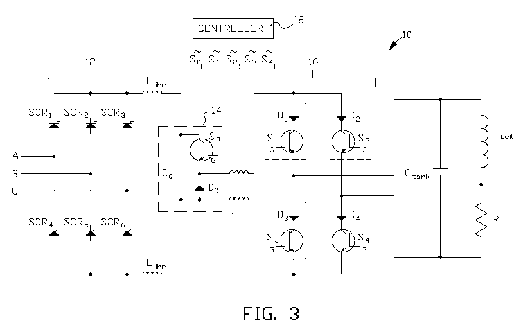
[0018] FIG. 3 is a simplified schematic diagram of one example of a power
supply with a
current fed inverter of the present invention connected to a resonant load.
[0019] FIG. 4 is a simplified schematic diagram of another example of a power
supply of the
present invention wherein multiple current fed inverters, each individually
regulated, are each
connected to a different resonant load and a single rectifier.
[0020] FIG. 5 is a simplified schematic diagram of another example of a power
supply of the
present invention wherein multiple current fed inverters, regulated by a
common regulator, are
each connected to a different resonant load and a single rectifier.
[0021] FIG. 6(a) and FIG. 6(b) graphically illustrate single pulse and multi-
pulse regulator
performance for one example of the current fed inverter power supplies of the
present invention.
[0022] FIG. 7(a) and FIG. 7(b) graphically illustrate parameters at unity duty
cycle/resonance
and unity duty cycle/off resonance of one example of the current fed inverters
of the present
invention.
[0023] FIG. 8 is a simplified schematic diagram of another example of a power
supply with a
current fed inverter of the present invention.
[0024] FIG. 9(a) and FIG. 9(b) are diagrammatic illustrations of an electric
induction heating,
melting and stirring arrangement using power supplies shown in FIG. 8.
3
CA 02680094 2009-09-03
WO 2008/124655 PCT/US2008/059512
[0025] FIG. 10(a) and FIG. 10(b) are simplified schematic illustrations of an
electric induction
heating, melting and stirring arrangement using the power supply shown in FIG.
8.
[0026] FIG. 10(c) is an illustration of one example of a diode bridge switch
used in the
arrangement shown in FIG. 9(a), FIG. 9(b) and schematics of FIG. 10(a) and
FIG. 10(b).
[0027] FIG. 11(a) is an illustration of one arrangement of the present
invention for electric
induction stirring.
[0028] FIG. 11(b) is an illustration of one example of the present invention
where the convex
meniscus surface of molten metal material in the crucible is modulated.
[0029] FIG. 12(a) and FIG. 12(b) respectively illustrate typical designating
conventions for
wound and counter-wound coil configurations.
Detailed Description of the Invention
[0030] One example of the power supply 10 of the present invention is
illustrated in FIG. 3. The
power supply comprises three active sections, namely rectifier 12, power
regulator 14 and current
inverter 16. Optional interharmonic reduction elements, illustrated in FIG. 3
as passive inductors
(chokes), L;i,r, connect the dc output of the rectifier to the power
regulator. Energy storage
elements, illustrated in FIG. 1 as passive inductors (chokes), L;, connect the
output of the power
regulator to the input of the inverter.
[0031] Input to three-phase rectifier 12 is from a suitable ac source, for
example, 50 or 60 Hertz
utility power (designated as lines A, B and C in the figure). Rectifier 12
comprises a full-wave
phase-controlled rectifier comprising six switch devices, such as silicon
controlled rectifiers
SCRi through SCR6 in this non-limiting example. In other examples of the
invention the rectifier
may be of a half-wave phase-controlled design, or other suitable type. As
further explained
below, the rectifier operates as a constant voltage rectifier except for soft
start of the power
supply to prevent initial overcharge of the regulator's energy storage device,
which is represented
by capacitive element, Co, in FIG. 3.
[0032] Inverter 16 comprises four switch devices, which in this non-limiting
example are
configured as an H-bridge. Each switch device is symbolically illustrated as
an insulated gate
bipolar transistor (IGBT) in series with a diode, although other types of
switch devices and
bridge configurations may be used in other examples of the present invention.
Generally in
steady state operation, inverter switch pair Si and S4 conduct for an
electrical half cycle (that is,
positive half cycle) and inverter switch pair S2 and S3 conduct for the
following electrical half
4
CA 02680094 2009-09-03
WO 2008/124655 PCT/US2008/059512
cycle (that is, negative half cycle), to deliver ac current to a resonant load
circuit, which may
comprise an electric induction furnace, or heating coil, diagrammatically
represented by
inductive element L,o;i, in series with resistive element R generally
representing the impedance of
the magnetically coupled load being melted or heated; and tank (resonant)
capacitor Ctaõk
connected in parallel with the series combination of L,o;i and R to form an
"RLC" resonant load.
As the resonant load impedance changes, the output frequency of inverter 16 is
adjusted by
controller 18 to keep the inverter operating at or near resonance to maximize
power transfer to
the resonant load circuit by gating control of the inverter's switch devices.
[0033] Controller 18 controls the duration and frequencies of the inverter's
switch devices and
regulator switch device So, which is also symbolically illustrated as an IGBT,
but may be any
other suitable type of switch device. In the power supply of the present
invention, regulator 14 is
synchronized with the output frequency of the inverter by controller 18 so
that the period of
regulator 14 (regulator period) is held at one half the period of the ac
output frequency of
inverter 16. Typically inverter 16 will operate at a frequency approximately
in the range of 100
Hertz to 1,000 Hertz for an application related to use of an industrial
electric induction furnace or
induction heating coil arrangements for heating electrically conductive
materials. Consequently
regulator 14 will operate with a period approximately in the range of 5 ms
(1/100 Hertz) to 0.5
ms (1/1,000 Hertz).
[0034] While regulator 14 operates at one half the period of inverter 16,
regulator 14 operates
with a variable duty cycle within the regulator period in steady state
operation. For example
regulator switch So may be conducting for only 80 percent of the regulator
period (.8 duty cycle),
during which time, regulator energy storage device, which in this non-limiting
example is
represented by energy storing inductor (choke), L;, charges from capacitive
element Co, which is
continuously charged from rectified utility power. During the regulator period
when So does not
conduct (switch device So open), current is supplied to the inverter from
energy stored in chokes
L. The magnitude of the output power is controlled by the duty cycle of switch
So; that is, the
ratio of the time period that switch So is in the on, or conducting state, to
the time period that the
switch is in the off or non-conducting state. As the duty cycle decreases, the
ac current ripple
component of the dc inverter input current supplied from chokes L; increases;
consequently, if a
single regulator pulse is used in every regulator period, choke Li must be
designed as a high
storage capacity choke with a large value of electrical inductance, and
consequently, a large
physical size. In order to minimize the size of the choke, at lower duty
cycles, multiple on/off
regulator pulses are provided in the regulator period in some examples of the
present invention.
5
CA 02680094 2009-09-03
WO 2008/124655 PCT/US2008/059512
[0035] The magnitude of current flowing through regulator switch So at low
duty cycles is
significantly less than the current flowing through regulator switch So at
high duty cycles.
Consequently switching losses in switch So will be lower at low duty cycles.
In the present
invention, the lower switching losses at low duty cycles is taken advantage of
by providing
current to the inverter in multiple on/off pulses within the regulated period
of the regulator to
provide the same magnitude of current ripple as the current ripple that would
be supplied with a
single low duty cycle pulse. This arrangement allows significant reduction in
the required
electrical rating of choke L; since more frequent pulses at low duty cycle
require significantly
less energy storage capacity in choke L; since that stored energy will be the
source of current to
the inverter when switch device So is not conducting for shorter intervals. A
suitable, but
non-limiting, control algorithm is as follows:
[0036] N = W" aX - Wcond
WSW
[0037] where N equals the number of allowed regulator pulses in a regulator
period;
[0038] Wm,,x equals the maximum allowed power dissipation specified for a
selected regulator
switch So;
[0039] W,oõd equals the conduction losses specified for a selected regulator
switch So; and
[0040] WsW equals the calculated switching losses with a single regulator
on/off duty cycle pulse
in a regulator period.
[0041] Therefore, for example, for a desired inverter output power magnitude
at resonance
requiring a single regulator on/off duty cycle of 0.3, WsW is calculated for
switch So current for
0.3 duty cycle, and maximum N at 0.3 duty cycle is calculated from the above
equation using
specified WmaX and W,oõd for the selected switch So.
[0042] By way of illustration and not limitation, FIG. 6(a) and FIG. 6(b)
graphically illustrate
single pulse versus multi-pulse regulation, for example, at 0.3 duty cycle. In
both figures, t;,,,
represents the period of inverter's output frequency, and treg represents the
period of the regulator,
which is one half the period of the inverter's output frequency. In FIG. 6(a)
single regulator pulse
in each regulator period, treg, is not preferred, as explained above; multiple
regulator pulses, as
illustrated by regulator pulses in FIG. 6(b) are preferred. The number of
pulses in a regulator
period will vary depending upon the range of required inverter current and
switch losses of a
particular regulator switch used in an application. Five regular pulses are
used in FIG. 6(b) for
6
CA 02680094 2009-09-03
WO 2008/124655 PCT/US2008/059512
clarity. Generally the number of pulses per regulator period may vary from two
to hundreds, in a
duty cycle range from less than unity to greater than zero, respectively.
[0043] If more inverter output power is required than that with a duty cycle
of 1.0 at resonance,
additional output power can be provided by increasing the output frequency of
the inverter,
which will supply more power but not at resonance. FIG. 7(a) and FIG. 7(b)
graphically
illustrate inverter parameters at unity duty cycle/resonance and unity duty
cycle/off resonance,
respectively, when greater inverter output power can be provided. FIG. 7(a)
illustrates inverter
resonant output power magnitude of P2, which is greater than power magnitude
Pi, with duty
cycle equal to 1.0 at resonance. FIG 7(b) illustrates inverter off-resonant
output power
magnitude of P3, which is greater than power magnitude P2, with duty cycle
equal to 1.0 and a
phase shift (o) between the inverter's output current and voltage.
[0044] For a non-vacuum electric induction furnace application, components of
a power supply
with the current fed inverter of the present invention would generally be
fully rated for maximum
power output in the off-resonance power range; for a vacuum electric induction
furnace
application, components of a power supply with the current fed inverter of the
present invention
would generally be fully rated for maximum power at resonant, unity duty cycle
operation.
[0045] In another example of a power supply with current fed inverters of the
present invention,
as illustrated in FIG. 4, multiple inverters 16 and 16', each with a dedicated
regulator switch (So
and S'o) and diode (Do and D'o), can be powered from single rectifier 12 and
energy storage
device, capacitor Co, that is connected to the output of the rectifier. In
this arrangement,
controlled, apportioned distribution of power among multiple resonant loads
LOAD 1 and
LOAD 2 can be accomplished by individual pulse regulation of inverters 16 and
16' as described
above, subject to a maximum total power output established by the rating of
rectifier 12. While
two inverter/load circuits are shown in FIG. 4, any number of inverter/load
circuits can be used.
[0046] In another example of a power supply with current fed inverters of the
present invention,
as illustrated in FIG. 5, multiple inverters 16 and 16', each serving
dedicated resonant loads
LOAD 1 and LOAD 2, respectively, can be selectively powered from single
regulator 14, which
is connected to the output of a rectifier operating at full-wave output as
described above. With
switches Si, S3, S'i and S'4 conducting, and switches S2, S4, S'2 and S'3 not
conducting, current is
supplied to LOAD 2, but not applied to LOAD 1, for example, for an electrical
half-cycle; while
in the next electrical half-cycle, switches S2, S4, S'2 and S'3 are
conducting, and switches Si, S3,
S'i and S'4 are not conducting to continue supply of current to LOAD 2.
7
CA 02680094 2009-09-03
WO 2008/124655 PCT/US2008/059512
[0047] While the switching schemes are generally described above for inductive
heating and
melting, in other examples of the invention, the switching schemes may be used
to affect induced
stirring patterns when used as an inverter in an induction furnace
application. Such an
application is illustrated in the non-limiting example shown in FIG. 8, FIG.
9(a) and FIG. 9(b).
FIG. 8 is one example of ac power supplies 20a, 20b and 20c that are used to
supply power to
each one of three induction coils, namely lower coi122a, middle coi122b and
upper coi122c,
which surround crucible 90. Tank capacitors CTi, CT2 and CT3 are provided at
the output of each
power supply. Each capacitor may have a different capacitance value. Resistive
elements Ri, R2
and R3 represent the resistance of a magnetically coupled load being heated,
melted or stirred in
crucible 90 that is surrounded by each coil section. Switches SWi and SW2 are
used to balance
coil currents when the switches are closed in the melt mode as shown in FIG.
9(a). With both
SWi and SW2 closed the established orientation of magnetic flux is as
illustrated by typical flux
line 94. One advantage of this arrangement is that each switch may have a
continuous current
rating of approximately 10 percent of the full current (power) rating of the
crucible since the
impedance of the induction coil sections of the furnace are similar in value,
with a typical
deviation between coils of less than 10 percent. Switches SWi and SW2 may be
of a mechanical
or electrical type. Switches SWi and SW2 may be combined into one suitably
arranged switching
device. A typical, but non-limiting, electronic switch is illustrated in FIG.
10(c), as a diode
bridge SCR switch. The current between coil sections is relatively low, which
favors the
application of electronic switching devices. With the operating conditions
identified above, the
induced electromagnetic stir pattern can be represented by exemplary flow
lines 92a in FIG. 9(a),
which is a double vortex ring, or toroidal vortex flow pattern with separate
vortex rings in the
lower and upper halves of the crucible.
[0048] More generally each induction coil in FIG. 9(a) and FIG. 9(b) may be
defined as having a
first, or "start," end termination, and a second, or "end," end termination.
For example in
FIG. 12(a) if induction coi170 represents a wound (right to left rise around
crucible 90) oriented
induction coil, and in FIG. 12(b) induction coi172 represents a counter-wound
(left to right rise
around crucible 90) oriented induction coil, start and end terminals of each
coil can be designated
as shown in the figures. Alternatively as shown in FIG. 9(a) and FIG. 9(b),
the start terminals of
induction coils 22a, 22b and 22c can be designated with a "circled star"
symbol as shown in the
figures, indicating, for example, in this non-limiting example of the
invention, that coi122a and
22c are wound oriented and coi122b is counter-wound oriented, or vice versa.
Using this
convention, the start terminals of all three induction coils are selectively
connected together only
when switches SWi and SW2 are closed, while the end terminals of all three
induction coils are
8
CA 02680094 2009-09-03
WO 2008/124655 PCT/US2008/059512
always connected together in common. In other examples of the invention, more
than three
induction coils may be used, with the start terminals of all of the induction
coils selectively
connected together by one or more switching devices, and the end terminals of
all of the
induction coils always connected together in common, or vice versa.
[0049] In stir mode any two of the three power supplies may be set to
quiescent state with the
outputs from the two of the three power supplies being zero so that the tank
capacitor, resistance
and coil section associated with each quiescent state power supply forms a
parallel RLC circuit.
In stir mode both SWi and SW2 are opened. In FIG. 9(b) and FIG. 10(b) power
supply 20a is
selected as active and power supplies 20b and 20c are in the off or quiescent
state (illustrated by
drawing these two power supplies in dashed lines). Consequently output current
from power
supply 20a flowing through coi122a generates a magnetic field represented by
typical flux
line 98a. This magnetic field couples (diagrammatically represented by "M")
with the RLC
circuit formed by coi122b, resistance R2 and capacitor CT2, which in turn,
results in an induced
current flow through coi122b that generates a secondary magnetic field
represented by typical
flux line 98b. The secondary magnetic field couples with the RLC circuit
formed by coi122c,
resistance R3 and capacitor CT3, which in turn, results in an induced current
flow through coi122c
that generates a secondary magnetic field represented by typical flux line
98c. The combination
of these magnetic fields will induce an electromagnetic flow pattern in molten
electrically
conductive material in the crucible as shown in FIG. 9(b). The induced
electromagnetic stir
pattern can be represented by exemplary flow lines 92b in FIG. 9(b) to create
a single vortex ring
flow pattern in the crucible with a downward flow pattern about the poloidal
(circular) axis Z of
the ring, or counterclockwise poloidal rotation. This stir arrangement is
particularly useful when
adding additional charge to the melt, such as metal chips 94, as illustrated
in FIG. 11(a), so that
the added charge is drawn quickly into the melt. The poloidal rotation may be
reversed to
clockwise by activating power supply 20c and deactivating power supplies 20a
and 20b. In some
examples of the invention, alternating or jogging the output power level of
the upper power
supply 20c can be used to agitate (modulate) the height of the convex meniscus
80 that defines
the surface of the molten metal bath, for example, from meniscus 80 to 80a as
shown in
FIG. 11(b), to expose a greater molten metal surface area to the ambient
atmosphere. This is of
particular value when the application is a vacuum furnace and the ambient
atmosphere is a
vacuum. Increasing the molten metal surface area exposed to the vacuum above
the surface,
increases the efficiency of the outgassing.
[0050] The example of the invention shown in FIG. 9(a) and FIG. 9(b) may be
used in both
vacuum and non-vacuum induction furnace applications and either in a batch
process, where the
9
CA 02680094 2009-09-03
WO 2008/124655 PCT/US2008/059512
crucible is initially filled with solid and/or semisolid electrically
conductive material, or a heel
process, where electrically conductive solid or semisolid charge is gradually
added to the existing
heel at the bottom of the crucible. Typically the melt and heat mode (FIG.
9(a) and FIG. 10(a)) is
used to initially melt all of the electrically conductive material in the
crucible. Then the stir mode
(FIG. 9(b) and FIG. 10(b)) is used, for example, to enhance conduction heating
through the
molten bath; and/or to promote degassing of the molten bath by circulating the
molten bath
volume so that the surface of the molten bath is continuously changing to
promote gas transfer
from the melt to the ambient atmosphere or vacuum; and/or to promote
dissolving additional
charge added to the molten bath by drawing it into the downward central vortex
identified as axis
Z in FIG. 9(b).
[0051] Although three induction coil sections are shown in the above examples
of the invention,
other quantities of coil sections may be used in other examples of the
invention.
[0052] The above examples of the invention have been provided merely for the
purpose of
explanation and are in no way to be construed as limiting of the present
invention. While the
invention has been described with reference to various embodiments, the words
used herein are
words of description and illustration, rather than words of limitations.
Although the invention
has been described herein with reference to particular means, materials and
embodiments, the
invention is not intended to be limited to the particulars disclosed herein;
rather, the invention
extends to all functionally equivalent structures, methods and uses such as
are within the scope of
the appended claims. Those skilled in the art, having the benefit of the
teachings of this
specification, may effect numerous modifications thereto, and changes may be
made without
departing from the scope of the invention in its aspects.