Note: Descriptions are shown in the official language in which they were submitted.
CA 02680132 2011-08-23
74769-2589
1
SOFTWARE PROGRAMMABLE LOGIC USING SPIN TRANSFER
TORQUE MAGNETORESISTIVE DEVICES
Field of Disclosure
[00021 Embodiments of the invention are related to a programmable logic array
(PLA)
or a field programmable gate array (FPGA). More particularly, embodiments of
the
invention are related to a PLA, FPGA or software programmable logic using Spin
Transfer Torque Magnetoresistive Random Access Memory (STT-MRAM) technology.
Background
[00031 A field-programmable gate array is a semiconductor device, which
includes
programmable logic components called "logic blocks" and programmable
interconnects.
Logic. blocks can be programmed to perform the function of basic logic gates
such as
AND, and XOR, or more complex combinational functions such as decoders or
simple
mathematical functions. In most FPGA's, the logic blocks also include memory
elements, which may be simple flip-flops or more complete blocks of memories.
A
hierarchy of programmable interconnects allows logic blocks to be
interconnected as
needed by the system designer. After the FPGA is manufactured, the system
designer
may use programming to implement many different logical functions, thereby
making
the device "field-programmable".
[0004] A PLA is similar to a FPGA, except that the PLA is modified, or
"programmed",
at the. fabrication stage of the integrated circuits by changes in one or two
masks. As
described in U.S. Patent 5,959,465, a PLA having flash EPROM memory elements
is
generally composed of two logic planes, an input plane and an output plane.
Each plane
receives inputs which are applied to gate terminals of transistors within the
logic plane,
and provides outputs to output nodes. The inputs to the input plane are the
inputs to the
PLA. The outputs of the input plane are intermediate nodes. The inputs to the
output
CA 02680132 2009-09-02
WO 2008/121973 PCT/US2008/058927
2
plane are connected to the intermediate nodes. The outputs of the output plane
are the
outputs of the PLA. The input plane may provide an AND function, and the
output
plane may provide an OR function. Alternatively, both planes may provide a NOR
function. These functions are defined by the type and connectivity of the
transistors
used and the signals applied to their gates. The NOR-NOR configuration has
particular
advantages in that it is the simplest to implement in CMOS logic. NOR stages
have a
number of transistors equal to the number of inputs connected in parallel.
Addition of
further parallel transistors for accommodating further inputs does not affect
the
operating speed of the stage.
[0005] U.S. Patent 6,876,228 describes a FPGA with magnetic storage elements
or
memory cells known as Magnetoresistive Random Access Memory (MRAM).
Connection information is written to the magnetic storage elements. The
connection
information is serially input and stored in shift registers, which correspond
to the
magnetic storage elements. When the power is switched on, the connection
information
stored in the magnetic storage elements is latched by latch elements, and is
output to
switching circuits to interconnect the logic blocks of the FPGA.
[0006] Magnetoresistive Random Access Memory (MRAM) is a non-volatile memory
technology that has response (read / write) times comparable to volatile
memory. In
contrast to conventional RAM technologies which store data as electric charges
or
current flows, MRAM uses magnetic elements. As illustrated in Figs IA and 1B,
a
magnetic tunnel junction (MTJ) storage element 105 can be formed from two
magnetic
layers 10 and 30, each of which can hold a magnetic field, separated by an
insulating
(tunnel barrier) layer 20. One of the two layers (e.g., fixed layer 10), is
set to a
particular polarity. The other layer's (e.g., free layer 30) polarity 32 is
free to change to
match that of an external field that can be applied. A change in the polarity
32 of the
free layer 30 will change the resistance of the MTJ storage element 105. For
example,
when the polarities are aligned, Fig. IA, a low resistance state exists. When
the
polarities are not aligned, Fig. 1B, then a high resistance state exists. The
illustration of
MTJ 105 has been simplified and those skilled in the art will appreciate that
each layer
illustrated may comprise one or more layers of materials, as is known in the
art.
CA 02680132 2011-08-23
74769-2589
3
SUMMARY
[0007] Exemplary embodiments of the invention are directed to systems,
circuits and methods for software programmable logic using Spin Transfer
Torque
Magnetoresistive technology.
[0008] An embodiment of the invention can include a programmable logic
array, comprising: a plurality of spin transfer torque magnetic tunnel
junction (MTJ)
devices, arranged in an array; and a plurality of programmable sources coupled
to
corresponding MTJ devices for changing the polarity of a free layer of each
MTJ
device; wherein a first group of the MTJ devices are arranged into an input
plane,
wherein a second group of the MTJ devices are arranged into an output plane,
and
wherein the input plane and the output plane are combined to form a logic
function
based on the relative polarities of the free layer of each MTJ device.
[0008a] Another embodiment can include a programmable logic array,
comprising: a plurality of spin transfer torque magnetic tunnel junction (MTJ)
devices,
arranged in an array; a plurality of programmable sources coupled to
corresponding
MTJ devices for changing the polarity of a free layer of each MTJ device;
wherein a
first group of the MTJ devices are arranged into columns and rows of an input
plane,
wherein a second group of the MTJ devices are arranged into at least one
column of
an output plane, wherein the input plane and the output plane are combined to
form a
logic function based on the relative polarities of the free layer of each MTJ
device;
and an output sense amplifier coupled to the output plane configured to detect
a
signal level on a column of the output plane and to generate a binary output
based on
a comparison of the signal level on the column of the output plane to a
threshold
signal level.
[0008b] Another embodiment can include a programmable logic array,
comprising: a plurality of spin transfer torque magnetic tunnel junction (MTJ)
devices,
arranged in an array; a plurality of programmable sources coupled to
corresponding
MTJ devices for changing the polarity of a free layer of each MTJ device;
wherein a
first group of the MTJ devices are arranged into columns and rows of an input
plane,
CA 02680132 2011-08-23
74769-2589
3a
wherein a second group of the MTJ devices are arranged into at least one
column of
an output plane, wherein the input plane and the output plane are combined to
form a
logic function based on the relative polarities of the free layer of each MTJ
device;
and a MUX driver coupled between the input plane and output plane, wherein the
MUX driver is configured to provide a read signal from a first row of the
input plane to
a MTJ of the output plane.
[0009] Another embodiment can include a method for implementing logic in an
array comprising: programming each of a plurality of spin transfer torque
magnetic
tunnel junction (MTJ) devices, arranged in an array to either a high or low
resistance
state, wherein each MTJ device is programmed by a first programmable source
coupled to a free layer side of a selected MTJ device and programmable source
coupled to a fixed layer side of the selected MTJ device; arranging a first
group of the
MTJ devices into columns and rows of an input plane; arranging a second group
of
the MTJ devices into at least one column in an output plane, wherein outputs
of each
row are coupled the MTJ devices in the at least one column; and determining a
logic
function based on the relative resistances of each MTJ device.
[0009a] Another embodiment can include a method for implementing logic in an
array comprising: programming each of a plurality of spin transfer torque
magnetic
tunnel junction (MTJ) devices, arranged in an array to either a high or low
resistance
state, wherein each MTJ device is programmed by a first programmable source
coupled to a free layer side of a selected MTJ device and programmable source
coupled to a fixed layer side of the selected MTJ device; arranging a first
group of the
MTJ devices into columns and rows of an input plane; arranging a second group
of
the MTJ devices into at least one column in an output plane, wherein outputs
of each
row are coupled to the MTJ devices in the at least one column; determining a
logic
function based on the relative resistances of each MTJ device; coupling a
plurality of
inputs, each input coupled to at least one MTJ device in corresponding input
columns
in the input plane; coupling a plurality of MTJ devices from different input
columns to
a first row in the input plane, wherein the first programmable source from the
programmable sources is coupled to the row; generating a voltage on the first
row by
CA 02680132 2011-08-23
74769-2589
3b
enabling the plurality of inputs and setting the first programmable source to
a low voltage
state; and generating a binary output voltage based on a comparison of the
voltage on
the first row to a threshold voltage.
[0009b] Another embodiment can include a method for implementing logic in an
array comprising: programming each of a plurality of spin transfer torque
magnetic
tunnel junction (MTJ) devices, arranged in an array to either a high or low
resistance
state, wherein each MTJ device is programmed by a first programmable source
coupled
to a free layer side of a selected MTJ device and programmable source coupled
to a
fixed layer side of the selected MTJ device; arranging a first group of the
MTJ devices
into columns and rows of an input plane; arranging a second group of the MTJ
devices
into at least one column in.an output plane, wherein outputs of each row are
coupled to
the MTJ devices in the at least one column; determining a logic function based
on the
relative resistances of each MTJ device; coupling output voltages of rows in
the input
plane to corresponding MTJ devices in a first column in the output plane;
setting a
programmable source coupled to the first column in the output plane to a low
voltage
state to establish a voltage on the first output column; and generating a
binary output
voltage for the output plane based on a comparison of the voltage on the first
column in
the output plane to a threshold voltage.
BRIEF DESCRIPTION OF THE DRAWINGS
[0010] The accompanying drawings are presented to aid in the description of
embodiments of the invention and are provided solely for illustration of the
embodiments
and not limitation thereof.
[0011] Figs. 1A and 1 B are illustrations of magnetic tunnel junction (MTJ)
storage
elements and their related states.
[0012] Figs. 1 C and 1 D are illustrations of Spin Transfer Torque
Magnetoresistive
Random Access Memory (STT-MRAM) bit cells.
[0013] Fig. 2 is an illustration of software programmable logic having an AND
input plane and an OR output plane using Spin Transfer Torque Magnetoresistive
technology.
CA 02680132 2009-09-02
WO 2008/121973 PCT/US2008/058927
4
[0014] Fig. 3A is an illustration of software programmable logic having a NOR
input
plane and a NOR output plane.
[0015] Fig. 3B is an illustration of a gate level implementation of the NOR -
NOR
programmable logic.
[0016] Fig. 4A is a schematic illustration of rows of the array of Fig. 3
using Spin
Transfer Torque Magnetoresistive technology.
[0017] Fig. 4B is an illustration of an equivalent circuit of the schematic of
Fig. 4A.
[0018] Fig. 5 is an illustration of programming the individual memory cells in
a logic
array.
[0019] Fig. 6A illustrates an example of the input circuit for a programmable
and
reconfigurable logic array using Spin Transfer Torque Magnetoresistive
technology.
[0020] Fig. 6B illustrates an example of a switchable power source used in the
circuit of
Fig. 6A.
[0021] Fig. 7 is a chart illustrating various voltage levels for signals for
an AND
configuration.
DETAILED DESCRIPTION
[0022] Aspects of embodiments of the invention are disclosed in the following
description and related drawings directed to specific embodiments of the
invention.
Alternate embodiments may be devised without departing from the scope of the
invention. Additionally, well-known elements of the invention will not be
described in
detail or will be omitted so as not to obscure the relevant details of
embodiments of the
invention.
[0023] The word "exemplary" is used herein to mean "serving as an example,
instance,
or illustration." Any embodiment described herein as "exemplary" is not
necessarily to
be construed as preferred or advantageous over other embodiments. Likewise,
the term
"embodiments of the invention" does not require that all embodiments of the
invention
include the discussed feature, advantage or mode of operation.
[0024] Embodiments of the invention use Spin Transfer Torque Magnetoresistive
Random Access Memory (STT-MRAM) elements to form part of the logic array. STT-
MRAM uses electrons that become spin-polarized as the electrons pass through a
thin
film (spin filter). STT-MRAM is also known as Spin Transfer Torque RAM (STT-
RAM), Spin Torque Transfer Magnetization Switching RAM (Spin-RAM), and Spin
CA 02680132 2011-08-23
74769-2589
Momentum Transfer (SMT-RAM). During the write operation, the. spin-polarized
electrons exert a torque on the free layer, which can switch the polarity of
the free layer.
The read operation is similar to conventional MRAM in that a current is used
to detect
the resistance / logic state of the MTJ storage element, as discussed in the
foregoing.
[00251 Referring now to FIG. IC, an example of a STT-MRAM bit cell 100 is
illustrated to aid in an explanation of programming MTJ 105. STT-MRAM bit cell
100
includes MTJ 105, transistor 110, bit line 120 and word line 130. The
transistor 110 is
switched on for both read and write operations to allow current to flow
through the MTJ
105, so that the logic state can be read or written. The logic state of the
MTJ 105 in the
STT-MRAM is written electrically, as opposed to a magnetic write in
conventional
MRAM.
[00261 Referring to FIG. 1D, a more detailed diagram of a STT-MRAM cell 101 is
illustrated, for further discussion of the read / write operations. In
addition to the
previously discussed elements such as MTJ 105, transistor 110, bit line 120
and word
line 130, a source line 140, sense amplifier 150, read / write circuitry 160
and bit line
reference 170 are illustrated. In contrast to MRAM, the write operation in an
STT-
MRAM is electrical. Read / write circuitry 160 generates a write voltage
between the
bit line 120 and the source line 140. Depending on the polarity of the voltage
between
bit line 120 and source line 140, the polarity of the free layer of the MTJ
105 can be
changed and correspondingly the logic state can be written to the cell 101.
Likewise,
during a read operation, a read current is generated, which flows between the
bit line
120 and source line 140 through MTJ 105. When the current is permitted to flow
via
transistor 110, the resistance (logic state) of the MTJ 105 can be determined
based on
the voltage differential between the bit line 120 and source line 140, which
is compared
to a reference 170 and then amplified by sense amplifier 150. The operation
and
construction of the memory cell 101 is known in the art. Additional details
are
provided, for example, in M. Hosomi, et al., A Novel Nonvolatile Memory with
Spin
Transfer Torque Magnetoresistive Magnetization Switching: Spin-RAM,
proceedings of
IEDM conference (2005).
[00271 Among other aspects, embodiments of the invention take advantage of the
low
power, static memory, and electrical read/write features of the STT technology
discussed above. Embodiments of the invention provide many features including:
extensible hardware; scalability through process generations;
reconfigurability; no
CA 02680132 2009-09-02
WO 2008/121973 PCT/US2008/058927
6
initialization; low standby leakage and state/program retention; small
dimensions; and
high speed.
[0028] For example, the implementation illustrated in FIG. 2 allows for the
realization
of a complex function derived from individual memory and logic components. As
illustrated in FIG. 2, software programmable function generation can be
accomplished
using the MTJ (e.g., 210) STT-MRAM cells in tandem with CMOS gates and
switching
supplies to allow for writable and readable "AND" (220) and "OR" (240) planes.
The
AND and OR plane topology facilitates full logic construction. For example,
the
function F0_B = X0_B + Xl_B can be realized (where _B denotes the complement
of a
given logic signal), as illustrated. Output FO_B (250) receives signals from
the
individual MTJ 210 storage elements coupled in the AND plane 220 which is
coupled
through MUX drivers 230 and an MTJ 210 storage elements to the OR plane 240.
The
AND plane 220 can include one or more AND bit lines 222 coupled to individual
MTJ
storage elements 210. A plurality of AND bit lines 222 can be combined to form
words
of arbitrary bit sizes. Likewise, OR plane 240 can include one or more OR bit
lines 242
coupled to MTJ storage elements 210 and a plurality of OR bit lines 242 can be
combined to form words of arbitrary bit sizes. A more detailed description of
the
topology and exemplary configurations will be provided in more detail in the
following
sections.
[0029] Fig. 3A illustrates a simplified schematic of a NOR-NOR PLA structure
300A.
The structure illustrated can perform the function FO = X 1 + X 2 + X 3 + X 4
. In
addition, an equivalent representation of the PLA logic in logic gates 300B is
provided
in Fig. 3B. The NOR-NOR configuration allows for both AND and OR operations to
be realized. For example, the function illustrated also performs the logical
function of
FO = XI = X2 + X3 = X4. Accordingly, complex positive and negative logic can
be
performed using basic inverters and gates or equivalent planes in the PLA, as
discussed
herein.
[0030] Referring to Fig. 4A, the NOR-NOR logic structure 300 can be
implemented
using STT technology in order to realize the function FO = XI = X2 + X3 = X4.
For
example, in the NOR-NOR structure 300, a plurality of STT-MTJs (e.g., 301 as
illustrated in Fig. 4A) can be coupled together in Rows 0 through Row N. There
are
evaluation circuits 302 at the inputs to Rows 0 to N, and an evaluation
circuit can also
be located at the output of the logic structure 300 (e.g., see Fig. 5). Each
of the
CA 02680132 2009-09-02
WO 2008/121973 PCT/US2008/058927
7
evaluation circuits includes a software programmable positive / negative (+/-)
source,
which can be set to the minimum voltage during read operations. The (+/-)
source can
be configured for either state for write / programming operations depending on
the state
to be written to the MTJs 301. The write / programming operation is described
in
greater detail below in relation to Fig. 5.
[0031] Each of the columns associated with MTJs 301 includes inputs which are
applied via lines X0, X0_B, Xl, Xl_B, . . XN, XN_B. There are drivers coupled
before
the inputs of the last STT-MRAM cells 301 in Rows 0-N, and an inverting sense
amp
310 at their output. The output of the inverting sense amp 310 provides the
function
realized by each row. Accordingly, the output of the row will be inverted
(e.g., a high
signal will result in a low output), which will be described in greater detail
below.
[0032] Fig. 4A is an example of a functional illustration of rows of the NOR-
NOR logic
structure 300 for read operations. Assuming the inputs Xl_B and X2_B
(alternatively
denoted as XI and X2 ) are the inputs of interest in Row 0, then the
resistance values of
MTJs in those rows can be set low by programming a "0" or setting the MTJ to a
parallel magnetization state. The remaining columns can be set to a high
resistance state
by programming a "1" or setting the MTJ to an anti-parallel magnetization
state.
Accordingly, a high logic value on either or both of Xl_B or X2_B will result
in a high
logic state on row 0. It will be appreciated that the values used herein are
merely for
illustration and other configurations may allow for a "0" to be a high
resistive state and
a "1" to be a low resistance state. Accordingly, embodiments of the invention
are not
limited to the illustrated configurations or associated values.
[0033] As illustrated schematically, MTJs 301 can be considered a programmable
resistance. The resistances of all the MTJs 301 along a given row can be
effectively
considered to yield an equivalent resistance RT, which in combination with the
effective
resistance of the evaluation circuit (Reval) can be represented as a voltage
divider 401,
in Fig. 4B, that will produce a voltage V,,;p (or a trigger voltage) on the
row for a given
input voltage at the inputs (e.g., .X1_B, X2_B, etc.) or from the equivalent
current from
the input columns. The voltage Vt;p can have a range for both high and low
depending
on the trip point of inverter 310, as illustrated in 402. Accordingly, circuit
design
considerations include adjusting the trip point low enough so that a single
high logic
state on an active input (e.g., Xl_B or X2_B) will be detected as a high and
cause the
output of inverting sense amp 310 to go low. Correspondingly, the trip point
can be
adjusted so any leakage current from the unused inputs (e.g., X3, X4, etc.) do
not cause
CA 02680132 2009-09-02
WO 2008/121973 PCT/US2008/058927
8
a false positive logic state to be activated. Since the complementary inputs
of Xl and
X2 are used in determining the state of Row 0 (e.g., the value of Vf;p) which
is input to
inverting sense amp 310, the output of inverting sense amp 310 is the function
Xl + X2
or XI = X2. Likewise, other functions can be realized for other rows and these
logical
functions can be combined into more complicated logical functions. It will be
appreciated that since both the inputs, outputs and their respective
complements (e.g.,
XO and X O) are available, the various desired functions can be DeMorganized
to be
achievable via the various logic planes (e.g., AND plane, OR plane, NOR
plane).
Further, since the MTJs 301 can be programmed to either a high or low
resistance the
functional logic of each plane can be reconfigurable.
[0034] Referring to Fig. 5, an illustration of programming the individual MTJs
210 is
provided. As discussed above, the MTJs 210 can be "programmed" to either a
relatively high resistance or low resistance state by setting the MTJ 210 to
an anti-
parallel or parallel magnetization state, respectively. Accordingly, for
purposes of
illustration, the high resistance state will be represented as a logic state 1
and the low
resistance state will be represented as a logic state 0. The programmable
array of Fig. 5
is similar to that illustrated in Fig. 2 so like reference numbers will be
used and a
detailed discussion of the elements will not be provided. As illustrated, each
MTJ 210
can be programmed by establishing a write path (e.g., 510) between software
programmable positive / negative (+/-) sources 512 and 514. Specifically, a
write
current can be sourced between the supplies 512 and 514 by placing the
remaining logic
paths (e.g., A to B) to a high impedance state and setting the supplies 512
and 514 to
the desired polarity to write a "1" or "0" state to the selected MTJ 210. It
will be
appreciated that this programming process can be repeated for all MTJs in the
AND
plane 220.
[0035] Likewise, MTJ 210 along write path 520 can be programmed by (+/-)
sources
522 and 524. Specifically, a write current can be generated between the
supplies 522
and 524 by placing the remaining logic paths in the OR Plane 240 to a high
impedance
state and setting the (+/-) sources 522 and 524 to the desired polarity to
write a "1" or
"0" state (e.g., a high resistance or low resistance state) to the selected
MTJ. As
illustrated, a portion (e.g., (a)) of the MUX driver 230 can be enabled to
allow for the
write operations and the read portion (e.g., (b)) can be set to a high
impedance state
during the write operations. It will be appreciated that the write portion (a)
of 230 can
CA 02680132 2009-09-02
WO 2008/121973 PCT/US2008/058927
9
allow for bidirectional current flow so that both states can be programmed
into the
selected MTJ. Also, it will be appreciated that the functionality of MUX
driver 230 can
be implemented as independent devices and embodiments of the invention are not
limited to the illustrated devices or topology. Accordingly, any device or
combination
of devices that can perform the functionality discussed above can be used in
place of
MUX driver 230.
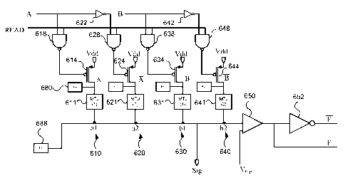
[0036] Fig. 6A illustrates an example of the input circuit for a STT
programmable logic
circuit. As illustrated, inputs A and B can be supplied to logic paths 610,
620, 630 and
640 to provide results for both the input A and B and their complements A and
B. In
the example illustrated, input A is provided to PMOS transistors 614 and is
inverted by
inverter 622 and provided to PMOS transistor 614 via NAND gates 618 and 628,
respectively. Likewise, input B is provided to PMOS transistors 634 and is
inverted by
inverter 642 and provided to PMOS transistor 644 via NAND gates 638 and 648,
respectively.
[0037] NAND gates 618, 628, 638 and 648 also receive an input from a READ
signal.
Accordingly, the NAND gates function to place the read logic paths 610, 620,
630 and
640 into a high impedance state when a read operation is not active. This
allows for the
independent programming of MTJs 611, 621, 631, 641, such as discussed in
relation to
Fig. 5. However, it will be appreciated that the NAND gate configuration is
provided
merely as an example and any suitable device can be used to achieve similar
functionality.
[0038] Accordingly, when input A has a high voltage level and the READ signal
is high
PMOS transistor 614 will be activated. As noted above, input A is also
supplied via
inverter 622 to PMOS transistor 624 which is activated in the opposite logic
state of the
path of 610 (e.g., activated on a low voltage of input A) so that the
complement to input
A is provided. In a similar manner when the READ signal is high, input B is
provided
to PMOS transistor 634 and also provided via inverter 642 to PMOS transistor
644 to
provide both B and its complement to paths 630 and 640, respectively.
[0039] As noted above, the logical state "1" or "0" (e.g., a high or low
resistance state)
of the STT Magnetoresistive devices (STT MTJs or MTJs) can be programmed into
each STT MTJ (e.g., 611, 621, 631, 641), using the associated software
programmable
positive / negative (+/-) sources 680 and 688, as discussed above. This
programmability
provides for a reconfigurable logic array in regard to logic functions of each
plane as
will be discussed in greater detail below. Also, as noted above, during the
programming
CA 02680132 2009-09-02
WO 2008/121973 PCT/US2008/058927
operations, the read path is placed in a high impedance state to allow for the
selection
and programming of each MTJ. Fig. 6B illustrates an example of (+/-) sources
680. As
illustrated, a programmable power supply 682 can be coupled to an Eval circuit
684
which allows for the programmable power source 680 to also be individually
enabled or
disabled. The Eval circuit 684 may be a CMOS device such as a transmission
gate or
any other device that allows for the individual coupling of the power source
682. The
activation of the Eval circuit 684 can be controlled by a WRITE X signal,
where X is
the column that is being written as each programmable source 680 can be
coupled to a
column of one or more MTJ cells (see, e.g., Fig. 5). Programmable source 688
can be
similarly configured as illustrated in Fig. 6B, however the Eval circuit will
be activated
on both read and write operations for each selected row. During the read
operation the
supply 682 would be set to the low voltage (which may be ground or a negative
voltage), so the resulting circuit would be similar to the read illustration
of Figs. 4A and
4B. Alternatively, programmable source 688 could have separate circuits for
read and
write. For example, the write portion could be configured as illustrated in
Fig. 6B and
the read portion could have an Eval circuit coupled directly to ground and
controlled by
the READ signal. Accordingly, it will be appreciated foregoing circuit
examples are
merely for illustration purposes and are not intended to limit the scope of
embodiments
of the invention.
[0040] In reviewing the topology of the programmable logic array, such as
illustrated in
Fig. 5, it will be appreciated that similar logic configurations can be used
for the output
plane (e.g., 240), where each MTJ in the output plane can be programmed to be
either a
low or high resistance and the output of each row can be supplied as the input
into each
corresponding MTJ. Likewise the programmable sources can be similar for
programming each of the MTJs in the output plane and the write portion of MUX
(e.g.,
230) can be used to select each MTJ to be written. Alternatively, individual
programmable sources can be supplied for each output MTJ and the corresponding
MUX could be simplified to only provide a read function. During the read
operation,
the result of the signals from the MTJs in the output plane can be can be
sensed by a
sense amplifier (e.g., 250) and set to either a logical 1 or 0 based on a
threshold as
discussed above, in relation to the read operation for each row.
[0041] To aid in an understanding of the operation of the various logic
configurations, a
truth table is provided below for input A for a given state of the related
MTJs 611 and
621. Specifically, as shown, when input A is in a high state (1), the values
at both nodes
CA 02680132 2009-09-02
WO 2008/121973 PCT/US2008/058927
11
al and a2 are a logical 0. Accordingly, the output F will be a logical 0 and
the
compliment of F will be a logical 1. In contrast when, input A is at a logical
0, the
value at node al remains a 0, but the value at node a2 is a logical 1, which
will result in
the output F being a logical 1 and the compliment of F will be a logical 0.
STT Logic Truth Table
Input MTJ Node Out Out
A State (al, a2) (F) (F_B)
1 0 (a1)
1 0 0 (a2) 0 1
1 0 (al
0 0 1 (a2) 1 0
Table 1
[0042] As illustrated, F is provided by buffering the voltage at Sig with
sense amplifier
650, which functions to switch from high to low once a given threshold or trip
/ trigger
level (e.g., Vf;p) is reached. Likewise, the complement of F is provided from
the output
of inverter 652. However, it will be appreciated that embodiments of the
invention are
not limited to this configuration. For example, the sense amplifier could have
an
inverted output and then be coupled in series with another inverter which
could be used
to provide inverted logic relative to the voltage at Sig and the complement of
the
inverted logic. It will further be appreciated that the use of logical values
such as 0 does
not imply that there is a zero voltage at node al or a2 but merely means that
the voltage
level at Sig is not sufficient to trigger a logical 1 as sensed at output F.
For purposes of
this explanation, it is assumed that paths 630 and 640 are in a high impedance
state and
do not contribute to the voltage at Sig. The impact of the various logic
levels are
discussed in greater detail below, in relation to Fig. 7.
[0043] Fig. 7 illustrates simulations for a logic configuration such as
illustrated in Fig.
6. The charts show the respective voltage levels for inputs A and B and can be
considered to have four quadrants that map to the four binary state
combinations of the
inputs (e.g., 10, 11, 01, 00). Further, a trigger / trip point value 732 can
be set to
determine the ultimate output state of that row of the array (see, e.g., Fig.
4B) based on
the Sig voltage 730 of the row feeding the sense amplifier. The output voltage
740 is
plotted to show the logic functioning for various input conditions. It should
be noted
that the sense amplifier for the output voltage 740 is assumed to be the
inverted output
for the graph illustrated. For example, if the Sig voltage 730 is below the
trigger point
CA 02680132 2009-09-02
WO 2008/121973 PCT/US2008/058927
12
voltage 732, then the output voltage 740 is high. Likewise, if the Sig voltage
730 is
above the trigger point voltage 732, then the output voltage 740 is low.
[0044] When input A is high and input B is low, the there will still be a
leakage path
through the STT MTJ devices and the voltage at Sig 730 will rise to a certain
level as
indicated in the first quadrant of the chart of Fig. 7. This value of Sig is
essentially
repeated in the third quadrant, where input A is low and input B is high. The
lowest
voltage level for Sig 730 occurs in the second quadrant when both inputs A and
B are
high. Due to the configuration of the logic array, such as illustrated in Fig.
6A, when
both inputs A and B are high, they are coupled to high resistance paths
through STT
devices 611 and 613 respectively. In contrast, when both A and B are low in
the fourth
quadrant, the highest voltage level for Sig 730 occurs, because both paths 620
and 640
will be active which have MTJs 621 and 641 set to a low resistive state.
Accordingly,
Sig 730 is greater than the trigger point 732 and the output 740 is low for
this condition.
It will be appreciated that the graph for the non-inverted output would result
in an
output graph having the opposite state. A truth table representation is
provided in Table
2 below for the graph of Fig. 7.
Input A Input B Output
1 0 0
1 1 1
0 1 0
0 0 0
Table 2
[0045] As discussed above, it will also be appreciated that the logic planes
can be
reconfigurable by reprogramming the values of the MTJs. For example, if the
values of
MTJs 611, 621, 631 and 641 are inverted then the logic realized by the row
illustrated in
Fig. 6A can be changed to an OR function. For example, if MTJs 611 and 631 are
programmed to the `0' or low resistance state, then the voltage on Sig will be
at an
elevated state when either input A or B is high and at its highest state when
both are
high. The voltage will be at its lowest state when both inputs A and B are
low.
Accordingly, the output of the row can realize an OR function as illustrated
in the truth
table represented in Table 3 below.
CA 02680132 2009-09-02
WO 2008/121973 PCT/US2008/058927
13
Input A Input B Output
1 0 1
1 1 1
0 1 1
0 0 0
Table 3
[0046] Accordingly, it will be appreciated that embodiments of the invention
include
both programmable and reconfigurable aspects using the STT MTJ devices in the
logic
array. Further, it will be appreciated that embodiments of the invention are
not limited
to the illustrated configurations. Embodiments of the invention can be
software
programmable via topology and arrangements and include, programmable decode
functions, extensible instruction sets, and on-the-fly hardware logic
addition/manipulation via software programming. Further, embodiments of the
invention can include designs that are executable in parallel without need for
a clock to
synchronize data transfer. Accordingly, using the STT MTJ devices, input
planes and
output planes and associated drivers as building blocks, embodiments of the
invention
can be configured to achieve complex functionalities.
[0047] While the foregoing disclosure shows illustrative embodiments of the
invention,
it should be noted that various changes and modifications could be made herein
without
departing from the scope of embodiments of the invention as defined by the
appended
claims. The functions, steps and/or actions of the methods in accordance with
the
embodiments of the invention described herein need not be performed in any
particular
order. Furthermore, although elements of the invention may be described or
claimed in
the singular, the plural is contemplated unless limitation to the singular is
explicitly
stated.