Note: Descriptions are shown in the official language in which they were submitted.
CA 02680752 2012-09-06
7 47 69-2 601
SPIN TRANSFER TORQUE MAGNETORESISTIVE RANDOM ACCESS MEMORY
AND DESIGN METHODS
Field of Disclosure
[00021 Embodiments of the invention are related to random access memory
(RAM).
More particularly, embodiments of the invention are related to memory design
in Spin
Transfer Torque Magnetoresistive Random Access Memory (STT-MRAM).
Background
100031 Random access memory (RAM) is a ubiquitous component of modem
digital
architectures. RAM can be stand alone devices or can be integrated or embedded
within
devices that use the RAM, such as microprocessors, microcontrollers,
application
specific integrated circuits (ASICs), system-on-chip (SoC), and other like
devices as
will be appreciated by those skilled in the art. RAM can be volatile or non-
volatile.
Volatile RAM loses its stored information whenever power is removed. Non-
volatile
RAM can maintain its memory contents even when power is removed from the
memory. Although non-volatile RAM has advantages in the ability to maintain
its
contents without having power applied, conventional non-volatile RAM has
slower read
/ write times than volatile RAM.
100041 Magnetoresistive Random Access Memory (MRAM) is a non-volatile
memory
technology that has response (read / write) times comparable to volatile
memory. In
contrast to conventional RAM technologies which store data as electric charges
or
current flows, MRAM uses magnetic elements. As illustrated in Figs 1A and 1B,
a
magnetic tunnel junction (MTJ) storage element 100 can be formed from two
magnetic
layers 110 and 130, each of which can hold a magnetic field, separated by an
insulating
(tunnel barrier) layer 120. One of the two layers (e.g., fixed layer 110), is
set to a
CA 02680752 2009-09-10
WO 2008/124704 PCT/US2008/059600
2
particular polarity. The other layer's (e.g., free layer 130) polarity 132 is
free to change
to match that of an external field that can be applied. A change in the
polarity 132 of
the free layer 130 will change the resistance of the MTJ storage element 100.
For
example, when the polarities are aligned, Fig. 1A, a low resistance state
exists. When
the polarities are not aligned, Fig. 1B, then a high resistance state exists.
The
illustration of MTJ 100 has been simplified and those skilled in the art will
appreciate
that each layer illustrated may comprise one or more layers of materials, as
is known in
the art.
[0005] Referring to Fig. 2A, a memory cell 200 of a conventional MRAM is
illustrated
for a read operation. The cell 200 includes a transistor 210, bit line 220,
digit line 230
and word line 240. The cell 200 can be read by measuring the electrical
resistance of
the MTJ 100. For example, a particular MTJ 100 can be selected by activating
an
associated transistor 210, which can switch current from a bit line 220
through the MTJ
100. Due to the tunnel magnetoresistive effect, the electrical resistance of
the MTJ 100
changes based on the orientation of the polarities in the two magnetic layers
(e.g., 110,
130), as discussed above. The resistance inside any particular MTJ 100 can be
determined from the current, resulting from the polarity of the free layer.
Conventionally, if the fixed layer 110 and free layer 130 have the same
polarity, the
resistance is low and a "0" is read. If the fixed layer 110 and free layer 130
have
opposite polarity, the resistance is higher and a "1" is read.
[0006] Referring to Fig. 2B, the memory cell 200 of a conventional MRAM is
illustrated for a write operation. The write operation of the MRAM is a
magnetic
operation. Accordingly, transistor 210 is off during the write operation.
Current is
propagated through the bit line 220 and digit line 230 to establish magnetic
fields 250
and 260 that can affect the polarity of the free layer of the MTJ 100 and
consequently
the logic state of the cell 200. Accordingly, data can be written to and
stored in the MTJ
100.
[0007] MRAM has several desirable characteristics that make it a candidate
for a
universal memory, such as high speed, high density (i.e., small bitcell size),
low power
consumption, and no degradation over time. However, MRAM has scalability
issues.
Specifically, as the bit cells become smaller, the magnetic fields used for
switching the
memory state increase. Accordingly, current density and power consumption
increase
to provide the higher magnetic fields, thus limiting the scalability of the
MRAM.
CA 02680752 2012-09-06
7 4 7 6 9 ¨ 2 6 0 1
3
[00081 Unlike conventional MRAM, Spin Transfer Torque Magnetoresistivc
Random
Access Memory (STT-MRAM) uses electrons that become spin-polarized as the
electrons pass through a thin film (spin filter). STT-MRAM is also known as
Spin
Transfer Torque RAM (STT-RAM), Spin Torque Transfer Magnetization Switching
RAM (Spin-RAM), and Spin Momentum Transfer (SMT-RAM). During the write
operation, the spin-polarized electrons exert a torque on the free layer,
which can switch
the polarity of the free layer. The read operation is similar to conventional
MRAM in
that a current is used to detect the resistance / logic state of the MTJ
storage element, as
discussed in the foregoing. As illustrated in Fig. 3A, a STT-MRAM bit cell 300
includes MTJ 305, transistor 310, bit line 320 and word line 330. The
transistor 310 is
switched on for both read and write operations to allow current to flow
through the MTJ
305, so that the logic state can be read or written.
[00091 Referring to Fig. 3B, a more detailed diagram of a STT-MRAM cell
301 is
illustrated, for further discussion of the read / write operations. In
addition to the
previously discussed elements such as MTJ 305, transistor 310, bit line 320
and word
line 330, a source line 340, sense amplifier 350, read / write circuitry 360
and bit line
reference 370 are illustrated. As
discussed above, the write operation in an STT-
MRAM is electrical. Read / write circuitry 360 generates a write voltage
between the
bit line 320 and the source line 340. Depending on the polarity of the voltage
between
bit line 320 and source line 340, the polarity of the free layer of the MTJ
305 can be
changed and correspondingly the logic state can be written to the cell 301.
Likewise,
during a read operation, a read current is generated, which flows between the
bit line
320 and source line 340 through MTJ 305. When the current is permitted to flow
via
transistor 310, the resistance (logic state) of the MTJ 305 can be determined
based on
the voltage differential between the bit line 320 and source line 340, which
is compared
to a reference 370 and then amplified by sense amplifier 350. Those skilled in
the art
will appreciate the operation and construction of the memory cell 301 is known
in the
art. Additional details are provided, for example, in M. Hosomi, et al., A
Novel
Nonvolatile Memory with Spin Transfer Torque Magnetorcsistive Magnetization
Switching: Spin-RAM, proceedings of IEDM conference (2005) .
100101 The
electrical write operation of STT-MRAM eliminates the scaling problem
due to the magnetic write operation in MRAM. Further, the circuit design is
less
complicated for STT-MRAM. However, because both read and write operations are
CA 02680752 2012-09-06
747 69-2 601
4
performed by passing current through the MTJ 305, there is a potential for
read
operations to disturb the data stored in the MTJ 305. For example, if the read
current is
similar to or greater in magnitude than the write current threshold, then
there is a
substantial chance the read operation may disturb the logic state of MTJ 305
and thus
degrade the integrity of the memory.
SUMMARY
[0011] Exemplary embodiments of the invention are directed to systems,
circuits and
methods for a reduced read voltage in a Spin Transfer Torque Magnetoresistive
Random
Access Memory (STT-MRAM).
[0012] Accordingly, an embodiment of the invention can include a method
for
designing Spin Transfer Torque Magnetoresistive Random Access Memory (STT-
MRAM) comprising: obtaining a characteristic curve for an access transistor;
determining a state() resistance and a state I resistance of a magnetic tunnel
junction
(MTJ) storage element, corresponding to a first and second state of the
memory;
determining a write voltage such that the operating points of both the first
state and
second state write operations intercept the characteristic curve in a
saturated region; and
determining a read voltage such that the operating points of both the first
state and
second state read operations intercept the characteristic curve in a linear
region.
[00131 Access Memory (STT-MRAM) having a plurality of bit cells, each
bit cell
comprising: a magnetic tunnel junction (MTJ) storage element having a state()
resistance and a statel resistance, corresponding to a first and second state
of the
memory; an access transistor coupled in series with the MTJ between a bit line
and a
source line, wherein a gate of the access transistor is coupled to a word
line; a supply
voltage (VDD) coupled to the bit line or source line during write operations;
and a read
voltage (VR) coupled to the bit line during a read operation, and wherein the
read
voltage is selected such that the access transistor operates in a linear
region during read
operations and wherein the access transistor operates in a saturation region
during write
operations.
CA 02680752 2012-09-06
74769-2601
[0014] Another embodiment of the invention includes a computer-
readable
medium having instructions for designing Spin Transfer Torque Magnetoresistive
Random Access Memory (STT-MRAM) stored thereon, wherein executing the
instructions on one or more processors causes the one or more processors to:
load
5 a characteristic curve for an access transistor; determine a state()
resistance and a
state1 resistance of a magnetic tunnel junction (MTJ) storage element,
corresponding
to a first and second state of the memory; determine a write voltage such that
the
operating points of both the first state and second state write operations
intercept the
characteristic curve in a saturated region; and determine a read voltage such
that the
operating points of both the first state and second state read operations
intercept the
characteristic curve in a linear region.
BRIEF DESCRIPTION OF THE DRAWINGS
[0015] The accompanying drawings are presented to aid in the
description of
embodiments of the invention and are provided solely for illustration of the
embodiments and not limitation thereof.
[0016] Figs. 1A and 1B are illustrations of a magnetic tunnel
junction (MTJ)
storage element.
[0017] Figs. 2A and 2B are illustrations of a Magnetoresistive Random
Access
Memory (MRAM) cell during read and write operations, respectively.
[0018] Figs. 3A and 3B are illustrations of Spin Transfer Torque
Magnetoresistive Random Access Memory (STT-MRAM) cells.
[0019] Fig. 4A is a simplified schematic representation of a STT-MRAM
cell.
[0020] Fig. 4B is a graph illustrating characteristic curves for a
word line
transistor and load line indicating various operating points.
CA 02680752 2012-09-06
74769-2601
5a
[0021] Fig. 5A is a graph illustrating a characteristic curve for a
word line
transistor and load lines indicating various read operating points in the
saturated
region.
[0022] Fig. 5B is a graph illustrating a characteristic curve for a
word line
transistor and load lines indicating various read operating points in the
linear region.
[0023] Fig. 6A is a graph illustrating a characteristic curve for a
word line
transistor and load lines indicating various write operating points in the
saturated
region.
[0024] Fig. 6B is a graph illustrating a characteristic curve for a
word line
transistor and load lines indicating various write operating points in the
linear region.
[0025] Fig. 7 is a graph illustrating a characteristic curve for a
word line
transistor and load lines indicating various read and write operating points.
[0026] Fig. 8 is a graph illustrating a characteristic curve for a
word line
transistor and load lines indicating various read and write operating points.
CA 02680752 2009-09-10
WO 2008/124704 PCT/US2008/059600
6
[0027] Fig. 9 is a flowchart illustrating a design method to determine
various operating
points of a STT-MRAM bit cell.
DETAILED DESCRIPTION
[0028] Aspects of embodiments of the invention are disclosed in the
following
description and related drawings directed to specific embodiments of the
invention.
Alternate embodiments may be devised without departing from the scope of the
invention. Additionally, well-known elements of the invention will not be
described in
detail or will be omitted so as not to obscure the relevant details of
embodiments of the
invention.
[0029] The terminology used herein is for the purpose of describing
particular
embodiments only and is not intended to be limiting of embodiments of the
invention.
As used herein, the singular forms "a", "an" and "the" are intended to include
the plural
forms as well, unless the context clearly indicates otherwise. It will be
further
understood that the terms "comprises", "comprising,", "includes" and/or
"including",
when used herein, specify the presence of stated features, integers, steps,
operations,
elements, and/or components, but do not preclude the presence or addition of
one or
more other features, integers, steps, operations, elements, components, and/or
groups
thereof
[0030] The word "exemplary" is used herein to mean "serving as an example,
instance,
or illustration." Any embodiment described herein as "exemplary" is not
necessarily to
be construed as preferred or advantageous over other embodiments. Likewise,
the term
"embodiments of the invention" does not require that all embodiments of the
invention
include the discussed feature, advantage or mode of operation.
[0031] As discussed in the background, STT-MRAM uses a low write current
for each
cell, which is an advantage of this memory type over MRAM. However, in
conventional designs cell read current can approach or be higher than the
write current
threshold and thus cause an invalid write operation / destructive read to
occur.
[0032] Referring to Fig. 4A, a simplified schematic of an STT-MRAM cell is
illustrated. The MTJ is represented by resistance (R) 410 and is in series
with the
access transistor 420 between the bit line (BL) and source line (SL). The cell
operation
can be considered to have three modes; Breakdown; Read; and Write. A large
cell
current difference between state and statel is desired for proper sensing
operation. In
the Write mode, the write operation is a bidirectional operation to write
state and
CA 02680752 2009-09-10
WO 2008/124704 PCT/US2008/059600
7
state 1 , as previously discussed. A low write current is used for low power
operation.
Some of the design challenges for this memory cell include that the read and
write
operations use the same path and are electrical. Accordingly, a destructive
read will
occur if the read current is greater than the minimum write current. Further,
the
Breakdown mode can occur if the voltage across the MTJ (e.g., Vm) during a
write
operation is higher than Vbreakdown= The voltage (V) is the sum of the voltage
across the
MTJ (Vm) and the drain-source voltage (VDS).
The voltage across the MTJ can be
determined as:
¨ V
/ =V m =V DS
11 R R 5
[0033] and the drain-source current (IDs) can be determined as function of
the gate-
source voltage (VGs), drain-source voltage (VDs), the transistor threshold
voltage (Vi),
and channel width to channel length ratio (W/L), which can be give as:
IDS = f (vGs 5v Ds 5v,W I L) =
[0034] The gate-source voltage (VGs) can be determined as:
VGS VWL VSL 5
[0035] where VwL is the voltage on the word line and VsL is the voltage on
the source
line. The drain-source voltage (VDs) can be determined as:
VDS VD VSL 5
[0036] where VD is the voltage at node D between the MTJ 410 and the
access
transistor 420. The voltage (V) can also be determined as:
V =V BL - Vsi, 5
[0037] where VBL is the voltage on the bit line. Additionally, the
conditions for the
linear region and saturation region of the access transistor can be defined
as:
Linear region: VGs ¨VT > Vas
Saturation region: VGs ¨VT
VDS
[0038] In addition to the simplified schematic, characteristic curves for
the access (or
word line) transistor 420 are provided in Fig. 4B. The characteristic curves
are a family
of curves, each of which is a plot of drain-source current (IDs) versus drain-
source
voltage (VDs) for a particular gate-source voltage (VGs). In addition to the
characteristic
curves a load line 450 is plotted. Load line 450 intersects the linear region
of the
characteristic curves at point 452 and a saturation region at point 454, as
can be seen
from Fig. 4B.
CA 02680752 2009-09-10
WO 2008/124704 PCT/US2008/059600
8
[0039] Fig. 5A illustrates a load line for the read operation of a state0,
520, and a load
line for the read operation of a statel, 510, for a given read voltage VR.
Load line 520
has a slope of 1/R0, where R0 is the state resistance of the MTJ. Likewise,
load line
510 has a slope of 1/R1, where R1 is the statel resistance of the MTJ. Both
lines
intersect the drain-source voltage (VDs) line at point VR and intersect the
saturated
portion of the access transistor curve at points 512 and 522, respectively.
Since both
states are operating in the saturated portion, the read current for state is
substantially
equal to the read current for statel (i.e., Io = II). Accordingly, if the read
operation
occurs in the saturated region then it will be difficult to detect the state
of the MTJ as
the read currents for both states will be similar.
[0040] The read mode operation can be designed to have a significant
current difference
between state and statel, if it is designed to operate in the linear region.
Fig. 5B
illustrates a load line for the read operation of a state 540 and a load line
for the read
operation of a statel 530 for a given read voltage VR and a given gate-source
voltage
(VGs). Load line 540 has a slope of 1/R0, where Ro is the state resistance of
the MTJ.
Likewise, load line 530 also has a slope of 1/R1, where R1 is the statel
resistance of the
MTJ. Both lines intersect the drain-source voltage line at point VR. However,
in this
configuration, the load lines intersect the linear portion of the access
transistor curve at
points 532 and 542 for R1 and Ro, respectively. By operating in the linear
portion
during the read operation, the read current for state can be greater than the
read current
for statel (i.e., Io > II), as can be seen from Fig. 5B. The design target of
having a
significant current difference between state and statel can be achieved.
Accordingly,
the state of the MTJ will be easier to detect based on the different currents
and read
errors can be reduced. Other factors can also increase the current difference,
such as a
smaller on-state resistance Ron of the word line (or access) transistor.
Additionally, the
difference between Ro and R1 will also tend to increase the current difference
during the
read operation.
[0041] In contrast to the read operation, the write operation can have a
similar current
magnitude for each state and preferably has as low a write current, as
possible reduce
power consumption. Load lines for the write operation are illustrated in Fig.
6A and
6B. In Fig. 6A, a load line for the write operation of a state 620 and a load
line for the
write operation of a statel 610 for a given write voltage Vw, is illustrated.
Load line
620 has a slope of 1/R0, where Ro is the state resistance of the MTJ.
Likewise, load
line 610 has a slope of 1/R1, where R1 is the statel resistance of the MTJ.
Both lines
CA 02680752 2009-09-10
WO 2008/124704 PCT/US2008/059600
9
intersect the drain-source voltage line at point Vw and intersect the
saturated portion of
the word line transistor at points 612 and 622, respectively. Since both
states are
operating in the saturated portion, the magnitude of the write current for
state() can be
substantially equal to the magnitude of the write current for statel (i.e.,
Iwo = Iwi = Iw).
[0042] Alternatively, Fig. 6B illustrates a load line that intersects in
the saturated region
for the write operation of a state() 640 and a load line for the write
operation of a statel
630 for a given write voltage Vw. Load line 640 also has a slope of 1/R0,
where Ro is
the state() resistance of the MTJ. Likewise, load line 630 also has a slope of
1/R1, where
R1 is the statel resistance of the MTJ. Both lines intersect the drain-source
voltage line
(VDs) at point Vw. However, in this configuration, the load lines intersect
the linear
portion of the word line transistor curve at points 632 and 642 for R1 and RD,
respectively. By operating in the linear portion during the write operation,
the
magnitude of the write current for state() is greater than the magnitude of
the write
current for statel (i.e., Iwo > Iwi), as can be seen from Fig. 6B. The large
current
difference is not needed in the write operation, so a design target is to have
the write
operation occur in the saturation region of the access transistor.
[0043] Fig. 7 illustrates an example of combined read and write operating
points and
related load lines in an exemplary design. In the illustrated example, the
gate-source
voltage (VGs) on the access transistor is considered to be constant so only
one curve 700
is plotted for VGs. In this design, a load line for the write operation of a
state() 720 and a
load line for the write operation of a statel 710 for a given write voltage Vw
are
illustrated. Once again, the load line 720 has a slope of 1/R0, where Ro is
the state()
resistance of the MTJ. Likewise, load line 710 has a slope of 1/R1, where R1
is the
state 1 resistance of the MTJ. Both lines intersect the drain-source voltage
line (VDs) at
point Vw and can be designed to intersect the saturated region at points 712
and 722 for
R1 and Ro, respectively. Accordingly, a consistent write current magnitude Iw
can be
obtained.
[0044] In the read operation, it is desired that there is a current
differential for the
different read states. Accordingly, a load line for the read operation of a
state() 740 and
a load line for the read operation of a statel 730 is plotted for a given read
voltage VR.
Load line 740 also has a slope of 1/R0, where Ro is the state() resistance of
the MTJ.
Likewise, load line 730 also has a slope of 1/R1, where R1 is the state 1
resistance of the
MTJ. It will be appreciated that these slopes generally correspond to the same
slopes
for the write operation. Both lines intersect the drain voltage line at a read
voltage VR.
CA 02680752 2009-09-10
WO 2008/124704 PCT/US2008/059600
By selecting an appropriate read voltage VR, the load lines can intersect the
linear
portion of the access transistor curve 700 at points 732 and 742 for R1 and
Ro,
respectively. By operating in the linear portion during the read operation, a
detectable
difference can be established between the read current for state and the read
current for
statel (i.e., IR > IRO, as can be seen from Fig. 7.
100451 The example illustrated in Fig. 7 achieves at least the following
design targets.
= Read operating point: Linear region of the access transistor
= Write operating point: Saturation region of the access transistor
= Read current is smaller than the Write current to prevent destructive
reads
[0046] As noted in the foregoing, the read operation occurs in the linear
region so the
read current for state is going to be greater than the read current for
statel (i.e., Jo > II).
Accordingly, a significant current difference between state and statel makes
it easier
to detect the state of the MTJ and read errors can be reduced. The greater the
current
difference between the read states, the more resilient the design will be to
process,
voltage and temperature (PVT) variations experienced by all circuits.
Likewise,
designing the write operations to occur in the saturation region at a higher
current than
either read currents (i.e., 1w >> Jo > Ii) can improve the tolerance PVT
variations, with
respect to the destructive read problem discussed in the foregoing. This can
be
achieved by having a greater write voltage (Vw) than the read voltage (VR), as
illustrated. The difference 750 between the write voltage and read voltage is
a design
parameter that can be determined based on the expected PVT variations and
access
transistor characteristic curves for a given design.
[0047] Fig. 8 is a generalized graph illustrating various read and write
operating points
according to embodiments of the invention. The elements of the graph can be
obtained
from various parameters of the STT-MRAM cell design. These parameters include
the
state (Ro) and state l(Ri) resistances of the MTJ and a characteristic curve
for the
access transistor for a given voltage (VGs), for example. The write voltage
(Vw) then
can be selected to intercept the saturation region and the read voltage (VR)
can be set to
intercept the linear region, base on the write and read load lines.
Additionally, the read
and write voltages can be set to ensure that the maximum read current (e.g.,
IRo) is less
than the write current (Iw) and a minimum write current to meet the design
targets
discussed above. The minimum write current (Iw.) can be determined by
considering
CA 02680752 2009-09-10
WO 2008/124704 PCT/US2008/059600
11
cell current, MTJ resistance variations, cell size and V. The minimum write
current can
be established to be greater than the calculated minimum write current.
[0048] A simple circuit design can be achieved using only one power supply
(e.g.,
supply voltage (VDD) and ground) and generating an intermediate voltage for
the read
voltage (VR). An exemplary configuration can have the following configuration:
. VDD, 0 and VR as voltage levels
= VwL ¨ VDD for both read and write
= VBL ¨ VDD (0) and VSL =0 (VDD) for write
= VBL ¨ VR and VsL =0 for read
[0049] In the foregoing, VDD is a supply voltage, VR is the read voltage,
VwL is the
word line voltage, VBL is the bit line voltage, and VsL is the source line
voltage. The
foregoing parameters uses only one DC voltage generator for VR. As noted
above, both
the bit line and the source line voltage is coupled to ground (0) or VDD
during the write
operations, depending on the state being written. The source line voltage is
set to
ground (0) during the read and the bit line is set to VR. The word line
voltage is coupled
to VDD for both read and write, when enabled. Accordingly, all operating
states can be
achieved with only VDD, VR and ground (0) as voltage levels. Appropriate
selection of
VDD and VR in combination of the characteristic curves of the access
transistor can
allow for the design targets discussed above to be achieved (i.e., read
operating point in
the linear region of the access transistor; write operating point in the
saturation region of
the access transistor; and read current being smaller than the write current)
with a
minimum number of DC voltages.
[0050] Accordingly, an embodiment of the invention can include a Spin
Transfer
Torque Magnetoresistive Random Access Memory (STT-MRAM) having a plurality of
bit cells. Each cell can include a magnetic tunnel junction (MTJ) storage
element
having a state0 resistance and statel resistances and an access transistor,
such as
illustrated in Fig. 4A.. The access transistor can be coupled in series with
the MTJ
between a bit line and a source line. A gate of the access transistor can be
coupled to a
word line (WL). A supply voltage (VDD) can be applied to the bit line or
source line
during write operations. The other line (bit line or source line) not coupled
to VDD can
be coupled to ground to permit the write operations for both states, as
discussed above.
A read voltage (VR) can be applied to the bit line during a read operation and
the source
line can be set to ground or 0 volts. Additionally, the WL can be coupled to
VDD during
both the read and write operations. As discussed above, the read voltage can
be selected
CA 02680752 2009-09-10
WO 2008/124704 PCT/US2008/059600
12
such that the access transistor operates in a linear region during read
operations and the
write voltage (VDD) can be selected so the access transistor operates in a
saturation
region during read operations.
[0051] In view of the foregoing it will be appreciated that methods for
performing the
various sequence of actions, steps, functions and/or algorithms are included
in
embodiments of the invention. Accordingly, referring to Fig. 9, an embodiment
of the
invention can include a method for designing Spin Transfer Torque
Magnetoresistive
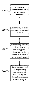
Random Access Memory (STT-MRAM) comprising: obtaining a characteristic curve
for an access transistor, 910. The state resistance and a statel resistance
of a magnetic
tunnel junction (MTJ) storage element can be determined, 920, corresponding to
a first
and second state of the memory. A write voltage can be determined, 930, such
that the
operating points of both the first state and second state write operations
intercept the
characteristic curve in a saturated region. Then, a read voltage can be
determined, 940,
such that the operating points of both the first state and second state read
operations
intercept the characteristic curve in a linear region. Additionally, a maximum
read
current is established to be less than a minimum write current.
[0052] Further, the effect of process, voltage and temperature (PVT)
variations can be
determined over a plurality of bit cells in a memory array. Each bit cell has
the MTJ,
an access transistor and similar write voltages and read voltages.
Accordingly, the
impact of PVT variations can be evaluated and the design can be evaluated to
ensure it
will successfully operate over the expected range of variation, which can be
determined
from information readily available to design engineers (e.g., characteristic
curves for
various access transistor designs) and by limits imposed by design engineers
(e.g.,
minimum and maximum operating voltage and temperature). If the original design
is
not determined to be acceptable, at least one of the state resistance, the
statel
resistance, the write voltage or read voltage can be adjusted based on the
determined
impact of the PVT variations and the process of Fig 9, for example, can be
repeated.
Additionally, a different access transistor design with different
characteristic curves can
be considered. Accordingly, a memory design can be determined such that each
of the
plurality of bit cells have write operations that intercept the characteristic
curve in the
saturated region and each of the read operations intercept the characteristic
curve in a
linear region.
[0053] The methods, sequences and/or algorithms described in connection
with the
embodiments disclosed herein may be embodied directly in hardware, in a
software
CA 02680752 2009-09-10
WO 2008/124704 PCT/US2008/059600
13
module executed by a processor, or in a combination of the two. A software
module
may reside in RAM memory, flash memory, ROM memory, EPROM memory,
EEPROM memory, registers, hard disk, a removable disk, a CD-ROM, or any other
form of storage medium known in the art. An exemplary storage medium is
coupled to
the processor such that the processor can read information from, and write
information
to, the storage medium. In the alternative, the storage medium may be integral
to the
processor. The processor and the storage medium may reside in an ASIC. The
ASIC
may reside in a user terminal. In the alternative, the processor and the
storage medium
may reside as discrete components in a user terminal. Accordingly, an
embodiment of
the invention can include a user terminal configured to perform the design
processes
described in the foregoing.
[0054] In one or more exemplary embodiments, the functions described may
be
implemented in hardware, software, firmware, or any combination thereof. If
implemented in software, the functions may be stored on or transmitted over as
one or
more instructions or code on a computer-readable medium. Computer-readable
media
includes both computer storage media and communication media including any
medium
that facilitates transfer of a computer program from one place to another. A
storage
media may be any available media that can be accessed by a computer. By way of
example, and not limitation, such computer-readable media can comprise RAM,
ROM,
EEPROM, CD-ROM or other optical disk storage, magnetic disk storage or other
magnetic storage devices, or any other medium that can be used to carry or
store desired
program code in the form of instructions or data structures and that can be
accessed by a
computer. Also, any connection is properly termed a computer-readable medium.
For
example, if the software is transmitted from a website, server, or other
remote source
using a coaxial cable, fiber optic cable, twisted pair, digital subscriber
line (DSL), or
wireless technologies such as infrared, radio, and microwave, then the coaxial
cable,
fiber optic cable, twisted pair, DSL, or wireless technologies such as
infrared, radio, and
microwave are included in the definition of medium. Disk and disc, as used
herein,
includes compact disc (CD), laser disc, optical disc, digital versatile disc
(DVD), floppy
disk and blu-ray disc where disks usually reproduce data magnetically, while
discs
reproduce data optically with lasers. Combinations of the above should also be
included
within the scope of computer-readable media.
[0055] Accordingly, an embodiment of the invention can include a computer-
readable
medium including code stored thereon for designing Spin Transfer Torque
CA 02680752 2009-09-10
WO 2008/124704 PCT/US2008/059600
14
Magnetoresistive Random Access Memory (STT-MRAM) comprising: code for causing
a computer to load a characteristic curve for an access transistor, code for
causing a
computer to determine a state resistance and a statel resistance of a
magnetic tunnel
junction (MTJ) storage element, corresponding to a first and second state of
the
memory, code for causing a computer to determine a write voltage such that the
operating points of both the first state and second state write operations
intercept the
characteristic curve in a saturated region, and code for causing a computer to
determine
a read voltage such that the operating points of both the first state and
second state read
operations intercept the characteristic curve in a linear region. Further, any
of the
functions describe herein can be included in as additional code in further
embodiments
of the invention.
[0056] While the foregoing disclosure shows illustrative embodiments of
the invention,
it should be noted that various changes and modifications could be made herein
without
departing from the scope of embodiments of the invention as defined by the
appended
claims. The functions, steps and/or actions of the methods in accordance with
the
embodiments of the invention described herein need not be performed in any
particular
order. Furthermore, although elements of the invention may be described or
claimed in
the singular, the plural is contemplated unless limitation to the singular is
explicitly
stated.