Note: Descriptions are shown in the official language in which they were submitted.
CA 02680861 2009-09-14
Engiish translation of W02008/114650
1
SPECIFICATION
CIRCUIT PROTECTION DEVICE
TECHNICAL FIELD
[0001]
The present invention relates to a circuit protection device
(or a circuit protection element). More specifically, it
relates to a circuit protection device comprising a bimetal
1o switch and a PTC component as well as an electrical circuit
(or an electrical apparatus) having such a circuit protection
device. Such a circuit protection device may be used as a
protection device in electrical circuits, which use various
high voltage or high current batteries, in electric vehicles,
cordless vacuum cleaners, power tools, wireless stations,
and the like, for example.
RELATED ART
(0002]
Circuit protection devices are incorporated into circuits for
various types of circuits in order to protect
electrical/electronic apparatuses and/or electrical/electronic
parts incorporated in such circuits in case voltage higher
than the rated voltage is applied to and/or current higher
than the rated current flows through the circuits.
CA 02680861 2009-09-14
English translation of W02008/114650
2
[0003]
As such a circuit protection device, using a bimetal switch
and a PTC component which are connected in parallel has
been proposed (see the Patent Reference below). With
such a circuit protection device, under normal operating
conditions, i.e. with voltage at or below the rated voltage and
current at or below the rated current, substantially all the
current flowing through the circuit will pass through contacts
in the bimetal switch; if, for example, there is an overcurrent,
1o the bimetal part of the bimetal switch will rise in temperature
to separate and open the contacts, and the current will be
diverted to the PTC component. As a result, the PTC
component will go into a high-temperature, high-resistance
state and trip due to the overcurrent, substantially cutting off
the current flow through the PTC component. At this point,
the high temperature of the PTC component maintains a
bimetal part at high temperature, so that the bimetal switch
maintains the opened state. In other words, the latch
condition of the bimetal switch is maintained. In such a
-20 circuit protection device, it is said that arcs do not occur at
the contacts of the bimetal switch since there is no need to
switch the current.
Patent Reference 1
Japanese Patent Kohyo Publication 11-512598
CA 02680861 2009-09-14
English translation of W02008/114650
3
DISCLOSURE OF THE INVENTION
PROBLEM TO BE SOLVED BY F THE INVENTION
[0004]
The present inventor, having closely studied the above
circuit protection device, has noticed that in a circuit
protection device wherein the PTC component is merely
connected in parallel to the bimetal switch, arcs may be
generated at the contacts in the bimetal switch, and in the
worst case, the contacts may be welded. When such
welding occurs, the device does not function as a circuit
protection device and cannot protect the electrical/electronic
apparatus and/or electrical/electronic parts incorporated into
the circuit. Therefore, the problem to be solved by the
present invention is to provide a circuit protection device as
above mentioned with a further improved potential to protect
circuits.
MEANS TO SOLVE THE PROBLEM
[0005]
The present invention provides a circuit protection device
comprising a bimetal switch and a PTC component,
characterized in that:
the bimetal switch and the PTC component are
electrically connected in parallel; and
CA 02680861 2009-09-14
English translation of W02008/114650
4
the PTC component has a resistance after its activation
that is equal to or less than 1.1 times (i.e. 1.1 x) as large as
a specific (or intrinsic) resistance of an electric circuit into
which the circuit protection device is to be incorporated,
which specific resistance is calculated based on a rated
voltage and a rated current of the electrical circuit according
to the fbllowing equation (1):
Rated Voltage/Rated Current = Specific Resistance (1).
1o EFEECTS OF THE INVENTION
[0006]
When the circuit protection device according to the present
invention is incorporated into an electrical circuit, the
formation of a welded portion at the contacts in the bimetal
switch may be further suppressed. As a result, the circuit
protection function of the circuit protection device is further
enhanced. Thus, the present invention further provides an
electric circuit into which the circuit protection device
according to the present invention is incorporated.
BRIEF DESCRIPTION OF THE DRAWINGS
[0007]
[Figure 1] Figure 1 shows a predetermined circuit A into
which a predetermined electrical apparatus (or part) B and a
bimetal switch C are incorporated.
CA 02680861 2009-09-14
Engiish translation of W02008/114650
[Figure 2] Figure 2 shows an electric circuit into which a
circuit protection device according to the present invention is
incorporated.
[Figure 3] Figure 3 shows a schematic side view of an
5 example of a more specific embodiment of a circuit protection
device according to the present invention.
[Figure 4] Figure 4 shows a schematic side view of an
example of a more specific embodiment of a circuit protection
device according to the present invention.
1o [Figure 5] Figure 5 shows a current wave profile and a
voltage wave profile measured in Example 1.
[Figure 6] Figure 6 shows a current wave profile and a
voltage wave profile measured in Example 2.
[Figure 7] Figure 7 shows a current wave profile and a
voltage wave profile measured in Example 3.
EXPLANATION OF THE REFERENCES
[0008]
1 - circuit protection device
2o 2 - PTC component
3 - circuit
4 - bimetal switch
6 - electric element
10, 10' - lead
12 - PTC component
CA 02680861 2009-09-14
English translation of W02008/114650
6
16 - bimetal switch
18, 18' - contact
20 - terminal section
22 - electrode layer
23 - PTC element
24 - electrode layer
26, 26' - insulating layer
30 - space
1o EMBODIMENTS TO CARRY OUT THE INVENTION
[0009]
Having studied why welding occurred at the contacts in the
bimetal switch, it has been concluded that the following
concept is a possibility. However, the present invention
described above and below is based on facts experimentally
confirmed by the present inventor. Therefore, this concept
is one of possibilities which are able to explain the present
invention, and whether the concept is appropriate or not does
not unduly limit the concept of the present invention.
[001 0]
The opening action of the contacts in a bimetal switch is
macroscopically an instantaneous action. However, when
such action is observed microscopically, it can be seen as an
action in which the contacts gradually separate from each
other in a very short period within such separation of the
CA 02680861 2009-09-14
English translation of W02008/114650
7
contacts. At the beginning of this very short period, a rated
current flows between the contacts, and at the end of such
very short period, current is interrupted between the contacts.
In other words, the resistance between the contacts at the
beginning of the very short period is substantially in the state
of zero, and at the end of such period, the resistance has
increased to be infinite. Therefore, the current flows and
the resistance increases greatly within this very short period,
so that electric power is consumed between the contacts.
1o [001 1 ]
On the other hand, it is possible to think that the
phenomenon of the bimetal contact welding occurs through
temperature rising of the contacts as a result of the effect of
excessive voltage and/or excessive current. Therefore,
when the energy consumed between the contacts becomes
great, the risk of welding occurring will increase.
[001 2]
In view of electric power being a measure of the energy, the
present inventor has therefore reached an idea in that the
occurrence or non-occurrence of welding between the
contacts can be determined by using the electric power, in
particular its maximum value, consumed between the
contacts in the above mentioned very short term as a
measure. This electric power consumption between the
contacts and its maximum value are calculated as explained
CA 02680861 2009-09-14
English translation of W02008/114650
8
below with reference to the circuit in Figure 1.
[001 3]
A predetermined circuit A is considered in Figure 1.
Typically into such a circuit, a predetermined electrical
apparatus (or part) B is incorporated in order that the circuit
functions as intended, and the circuit has a predetermined
resistance Rf. A bimetal switch C is also incorporated into
the circuit so that the circuit may be opened in case an
abnormal voltage is applied to and/or an abnormal current
1o flows through the circuit. A predetermined voltage E is
applied to the circuit.
[001 4]
As described above, the predetermined circuit is configured
such that the predetermined voltage is applied to the
electrical apparatus B so that a predetermined current flows
through the circuit. Such voltage and such current are
called a rated voltage Vr and a rated current Ir, respectively.
Such rated voltage and such rated current mean that, when
the voltage Vr is applied to the circuit, the current Ir flows
through the circuit, and therefore the circuit has a resistance
of Vr/Ir.
[001 5]
Therefore, when Vr/Ir = Rf, the circuit which is said to have
its rated voltage and its rated current of Vr and Ir
respectively corresponds to a circuit wherein E = Vr, and an
CA 02680861 2009-09-14
English translation of W02008/114650
9
electrical apparatus having a resistance of Vr/Ir as its
resistance (Rf) is incorporated in Figure 1. In other words,
the circuit A shown in Figure 1 is equivalent to a circuit
wherein its rated voltage and its rated current are Vr and Ir,
respectively (given that E = Vr, and I = Ir), and a specific
resistance of such a circuit is Vr/Ir.
[001 6]
In the circuit shown in Figure 1, it is assumed that the voltage
E is applied to the circuit, the electrical apparatus has a
1o resistance of Rf, and the bimetal switch has a resistance of
Rb as a resistance between the contacts. It is further
assumed that the voltage applied to the electrical apparatus
is Vf, and the voltage between the contacts of the bimetal
switch is Vb.
[001 7]
In this case, when it is assumed that the current flowing
through the circuit A is I and the whole circuit is considered,
the following is obtained:
I = E/(Rf+Rb).
[0018
]
When it is assumed that the electric power consumed
between the contacts of the bimetal switch is P, the following
is obtained:
P = IxVb.
[001 9]
CA 02680861 2009-09-14
English translation of W02008/114650
Since Vb = E-Vf, the following is obtained:
P = Ix(E-Vf)
[0020]
Since Vf = IxRf, the following is obtained:
5 P = Ix(E-IxRf) = IE-I2xRf
[0021 ]
When the electric power consumption of P which is expressed
as a function of I is differentiated with I, the following is
obtained:
10 P' = E-21xRf.
[0022]
Since P' becomes 0 when the electric power consumption
reaches the maximum, the following is obtained:
P' = E-2lxRf = 0.
When the current I at this point is assumed to be Imax, the
following is obtained:
Imax = E/(2Rf) = (1/2)x(E/Rf).
[0023]
When the Vb at this point is assumed to be Vmax, the
following is obtained:
Vmax = E-Vf = E-Imax x Rf = E-[E/(2Rf)] x Rf = E/2.
[0024]
In the above state, E/Rf is equal to the value of the current
flowing through the circuit when Rb is zero. It is impossible
that Rb becomes zero. However, when Rb may
CA 02680861 2009-09-14
English translation of W02008/114650
11
substantially be ignored in comparison with Rf, that is, when
the contacts of the bimetal switch are sufficiently touching to
be in a closed state, Rf>>Rb so that there is no problem in
that Rb is assumed to be substantialiy zero. Such a state
may be considered to be a state where the rated voltage Vr is
applied as the voltage E to the circuit A and the rated current
Ir is flowing through the circuit A.
[0025]
Thus, when the electric power consumption between the
1o contacts of the bimetal switch becomes the maximum, the
following is obtained:
Imax = E/(2Rf) = (1/2)x(Vr/Rf) = (1/2)xlr
Vmax = E/2 = (1/2)xVr
[0026]
Therefore, when the electric power consumption between the
contacts becomes the maximum, the current flowing between
the contacts becomes a half of the rated current, i.e. a
current of Ir/2, and the voltage applied between the contacts
becomes a half of the rated voltage, i.e. a voltage of Vr/2.
[0027]
In brief, the voltage and the current, when the electric power
consumption becomes the maximum between the contacts of
the bimetal switch which has been incorporated in series in a
predetermined circuit as a circuit protection device, will be
half values of the rated voltage and the rated current
CA 02680861 2009-09-14
English translation of W02008/114650
12
respectively of the circuit. Therefore, the resistance
between the contacts at this point is (Vr/2) /(Ir/2) = Vr/Ir =
Rated Voltage / Rated Current. In other words, this
resistance is a specific resistance of the circuit.
[0028]
It is presumed that, in the vicinity of this resistance, the
electric power consumption between the contacts becomes
the maximum, as a result of which arcing is likely to be
generated between the contacts thereby increasing the
1o possibility of the contact welding; thus this resistance (=
Vr/Ir) is also tentatively called "arcing resistance". It is
noted that the term "arcing resistance" used in this
specification is used only as a matter of convenience, and it
should be kept in mind that, although it is presumed that
there is some sort of correlation with the occurrence of the
arcing between the contacts, it cannot necessarily be
presumed that the resistance between the contacts becomes
this arcing resistance upon the occurrence of the arcing.
[0029]
2o The inventor has studied further and discovered
experimentally that, when the resistance of the PTC
component electrically connected in parallel to the bimetal
switch is equal to or less than the arcing resistance, the
possibility of welding occurring between the contacts is
reduced. The "resistance of the PTC component" as stated
CA 02680861 2009-09-14
English translation of W02008/114650
13
herein is a resistance (an electrical resistance) of the PTC
component after it has been connected in parallel to the
bimetal switch. When solder was used to connect a
commercially available PTC component to the bimetal switch,
the PTC component is in the state wherein it already tripped
once because of the heat caused by connecting with solder
(i.e. in the state after thermally tripping), and the present
specification calls the resistance of the PTC component in
this state as the "resistance of the PTC component". This
1o resistance is also called as a "resistance after activation" in
the technical field related to the present invention. It is
noted that when electric welding is used to connect the PTC
component to the bimetal switch, it may be possible that the
heat conducted to the PTC component is not enough to cause
tripping. In such a case, the PTC component will trip for
the first time when an overcurrent flows through the PTC
component for the first time (i.e. the PTC component tripping
electrically), and the resistance afterwards corresponds to
the "resistance after activation" as described above. In the
present invention, therefore, the "resistance after activation"
means the resistance after the commercially available PTC
component has tripped for the first time either thermally or
electrically. The PTC component before solder connecting
(i.e. the commercially available PTC component itself) has a
resistance smaller than such resistance (this smaller
CA 02680861 2009-09-14
English translation of W02008/114650
14
resistance is also called as a basic (or reference)
resistance" in the related art).
[0030]
As described previously, when incorporating into a
predetermined circuit a circuit protection device in which a
bimetal switch and a PTC component connected in parallel,
current which has flowed through the bimetal switch can be
shunted to the PTC component upon opening of the bimetal
switch. For example, in the case wherein a ratio of the
1o resistance of the PTC component to the specific resistance
(or the arcing resistance) of the circuit is equal to or less
than 1. 1, preferably equal to or less than 1.0, more
preferably equal to or less than 0.9, most preferably equal to
or less than 0.4, particularly equal to or less than 0.3, and
more particularly equal to or less than 0.2, for example equal
to or less than 0.15, a half of the current that would have
flowed between the contacts without the presence of the PTC
component can be shunted to the PTC component when the
electric power consumption between the contacts becomes
the maximum. As a result, the possibility of arcing between
the contacts is decreased. In the most preferred
embodiment, the ratio of the resistance of the PTC
component to the specific resistance (or the arcing
resistance) of the circuit is equal to or less than 0.2, and for
example equal to or less than 0.15. It is noted that in the
CA 02680861 2009-09-14
English translation of W02008/114650
circuit protection device according to the present invention,
the basic resistance of the PTC component is preferably
equal to or less than 4/5, and more preferably equal to or
less than 2/3 of the specific resistance (or the arcing
5 resistance), and for example equal to or less than 1/2 of the
specific resistance.
[0031 ]
Conversely, when the resistance of the PTC component is
larger than the arcing resistance of the circuit, for example
1o twice larger than the arcing resistance, the arc generation
may not be sufficiently suppressed even if a PTC component
has been incorporated in the circuit and welding may occur.
[0032]
In the circuit protection device according to the present
15 invention, the bimetal switch used in the circuit protection
device is a switch using a bimetal eiement, and a well-known
one may be used. This is a switch configured such that,
when current flowing through the bimetal switch exceeds a
predetermined current value and becomes excessive, the
contacts which are touching each other will separate by
means of generated heat.
[0033]
Among such bimetal switches, those, for example, that use
platinum, gold, silver, copper, carbon, nickel, tin, lead, or an
alloy of these metals (for example tin-lead alloy) as a contact
CA 02680861 2009-09-14
English translation of W02008/114650
16
material thereof may be given as examples of ones that are
particularly preferred for the use in the circuit protection
device according to the present invention. Above all, a
bimetal switch using silver as the contact material is
particularly preferred. It is noted that bimetal switches
having a relatively narrow gap between the contacts may
suitably be used in the circuit protection device of the
present invention. Such bimetal switch having a gap of
preferably 0.4 - 4 mm, in particular 2 mm or less, more
1o preferably 0.7 - 2 mm, particularly preferably 0.8 - 1.5 mm,
and for example around 1 mm may suitably be used in the
circuit protection device.
[0034]
The PTC component that is connected in parallel to the
bimetal switch in the circuit protection device according to
the present invention may be a conventional PTC component
that is itself used as a circuit protection device, and its
electrically conductive element may be made of a ceramic or
of a polymer material. A particularly preferred PTC
component is one that is called a polymer PTC component,
and a PTC component having an electrically conductive
polymer element in which an electrically conductive filler (for
example carbon, nickel, or nickel-cobalt filler) is dispersed in
a polymer material (for example a polyethylene, a
polyvinylidene fluoride, etc.) can be suitably used.
CA 02680861 2009-09-14
English translation of W02008/114650
17
[0035]
When the circuit protection device according to the present
invention is incorporated into a predetermined circuit and
performs its intended function normally, substantially all of
the current flowing through the circuit will pass through the
bimetal switch. Therefore, in the circuit protection device
according to the present invention, the resistance of the PTC
component has a resistance value that is at least 10 times,
preferably at least 50 times, more preferably at least 100
times, and particularly preferably at least 300 times as large
as the resistance that the bimetal switch inherently has
(normally 0.5 - 20 milliohms).
[0036]
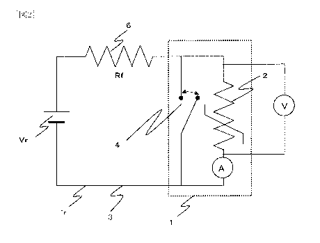
Figure 2 shows a circuit 3 into which the circuit protection
device 1 according to the present invention is incorporated.
The circuit 3 has a predetermined electrical element (e.g. an
electrical/electronic device or part, etc.) 6 and the circuit
protection device 1 is connected in series to the element.
The electrical element 6 is indicated with one resistance
symbol, but this denotes a single electrical element or a
group of a plurality of electrical elements included in the
circuit 3. The resistance of such an electrical element is
shown as Rf, which is a specific resistance of the circuit 3
and is calculated specifically by [the rated voltage (Vr) / the
rated current (Ir)] of the circuit 3. Figure 2 shows an
CA 02680861 2009-09-14
English translation of W02008/114650
18
ammeter A and a voltmeter V incorporated thereinto for the
purpose of measuring as explained below in the Examples.
[0037]
The circuit protection device 1 according to the present
invention comprises a PTC component 2 and a bimetal switch
4, which are electrically connected in parallel, or if not
electrically connected in parallel, are configured so that they
can be thus connected. A ratio of the resistance of the PTC
component 2 to the specific resistance Rf of the circuit 3 is
1o for example one or less, preferably one-half or less, more
preferably 1/3 or less, for example 1/4 or less, and in
particular 1/8 or less. Further, the PTC component has a
resistance of for example at least 10 times, and preferably at
least 100 times as large as the resistance that the bimetal
switch 4 inherentiy has.
[0038]
Specific embodiments of the circuit protection device 10
according to the present invention are shown as schematic
side views in Figure 3 and Figure 4.
[0039]
Figure 3 shows the states before and after (Figure .3(a) and
Figure 3(b)) the bimetal switch is activated so that the
contacts of the bimetal switch open in the circuit protection
device according to the present invention which has a PTC
component 12 and a bimetal switch 16 and which has been
CA 02680861 2009-09-14
English translation of W02008/114650
19
incorporated in an electrical circuit (only the leads 10 and 10'
of the electrical circuit are shown). The leads 10 and 10'
have terminal sections 20 and 20' at their ends respectively.
The terminal section 20 is connected to the terminal section
17 of the bimetal switch. When the circuit is operating
normally and appropriate current is flowing therethrough, i.e.
when current is flowing via the bimetal switch 16, the
terminal section 20' is in contact with the contact 18 of the
bimetal switch 16 as shown in Figure 3(a). In this state,
1o substantially all (or most) of the current flows from the lead
to the lead 10' via the bimetal switch 16.
[0040]
In the illustrated embodiment, the PTC component 12
comprises a PTC element 23 and electrode layers 22 and 24
disposed on both sides thereof, and an insulating layer 26 is
present between the PTC component 12 and the lead. The
PTC element and the electrode layers on both sides thereof
may be similar to those used in the known PTC components,
and the electrode layers may have leads on their outer
surfaces. In such embodiment, such PTC eiement forms, in
place of the shown PTC element 23, a PTC component
together with the electrode layers (preferably metal foil
electrodes) on the both sides of the PTC element, and also
forms leads on the above mentioned outer surfaces in place
of the shown electrode layers 22 and 24, which leads are
CA 02680861 2009-09-14
English translation of W02008/114650
connected to the leads 10 and 10' respectively. By
incorporating the PTC component 12 and the bimetal switch
16 in the electrical circuit as described above, an electrical
circuit is configured wherein these are electrically connected
5 in a parallel relationship. It is noted that in the shown
embodiment, another insulating layer 26' is disposed
between the bimetal switch 16 and the lead 10'.
[0041]
When an abnormal current flows through the electrical circuit
10 so that the temperature of the bimetal switch 16 rises, the
contacting state between the contact 18 and the terminal
section 20' is dissolved. At this point, the current flowing
through the electrical circuit flows instantaneously from the
lead 10 to the electrode layer 22 of the PTC component, and
15 shunts thereafter to the lead 10' via the PTC element 23 and
the electrode layer 24. In this case, when the resistance of
the PTC component after its activation is equal to or less
than 1.1 times (X 1. 1) as large as the specific resistance of
the circuit, a relatively large ratio of the abnormal current
20 can be shunted to the PTC component at the moment when
the bimetal switch opens, so that the possibility of an arcing
occurrence, welding occurrence or the like in the vicinity of
the bimetal switch contacts is greatly reduced. After this,
the PTC component will be in the trip state and substantially
cut off the current flow.
CA 02680861 2009-09-14
English translation of W02008/114650
21
[0042]
In Figure 3, the broken line surrounding the circuit protection
device according to the present invention denotes an element,
for example a casing, a housing or the like which surrounds
the circuit protection device. It is pr.eferable that the
protection device according to the present invention further
has such an element, which is useful in preventing
dissipation of heat (which is generated by the abnormal
current) from the bimetal switch and the PTC component, so
1o that the latched state of the bimetal switch can be maintained.
Further in the shown embodiment, since the PTC component
12 and the bimetal switch 16 are adjacent but separated by a
relatively narrow space 30 so that the heat from the PTC
component upon tripping thereof caused by the abnormal
current can easily affect the bimetal switch, such adjacent
condition is advantageous in maintaining the latched state of
the bimetal switch.
[0043]
Figure 4 also shows a further embodiment of the circuit
protection device according to the present invention in the
state before the bimetal switch is activated. In this
embodiment, the bimetal switch 16 and the PTC component
are separated from each other. A lead 10' as well as
insulating layers 26 and 26' are present between the bimetal
switch 16 and the PTC component 12, as a result of which,
CA 02680861 2009-09-14
English translation of W02008/114650
22
compared with the embodiment in Figure 3, the PTC
component 12 and the bimetal switch 16 are more separated
so that the bimetal switch is less likely to be affected by the
heat as previously explained. However, because the
bimetal component and the PTC component are configured by
merely overlapping one on the other, it is advantageous in
manufacturing the device.
Example 1
1o [0044]
Using a PTC component, a bimetal switch, and an electrical
element (a resistor, its resistance Rf = 2.67f2) which are
commercially available and described below, a circuit was
constructed shown in Figure 2 while incorporating the circuit
protection device into the circuit:
PTC component: manufactured by Tyco Electronics
Raychem, product name: RXE010, basic resistance: 2.6 0,
resistance after activation: 4.21 fl.
Bimetal switch: manufactured by Sensata Technologies,
product name: Thermal Protector 9700K21 -21 5, contact gap:
1 mm, resistance of bimetal switch: 11.6 ms2.
[0045]
DC 48V/18A (therefore the specific resistance = 2.67 0 = Rf)
which is double the maximum contact rating of the bimetal
switch was applied, and the wave profile of the current
CA 02680861 2009-09-14
English translation of W02008/114650
23
(current flowing through the bimetal switch) and the wave
profile of the voltage (voltage between the both ends of the
bimetal switch, i.e. the voltage drop across the bimetal
switch) upon such application were measured with the
ammeter A and the voltmeter V incorporated into the circuit
shown in Figure 2. Figure 5 shows the wave profiles of the
measured current and voltage (It is noted that the oscillating
wave profiles are shown smoothed out). In the graph in
Figure 5, the vertical axis denotes the voltage and current
1o value, each graduation (a length of two-ended arrow) thereof
being 5A and 10V, while the horizontal axis denotes time,
each graduation thereof being 40ms (millisecond).
[0046]
From Figure 5, it can be seen that about 146 ms after the
start of the contact opening action of the bimetal switch (time
= 0), the current and voltage values returned to those before
the opening action of the contacts. Thus, in this Example,
the circuit protection device did not perform its function.
When the bimetal switch was checked, there was welding at
the contacts.
Example 2
[0047]
Except that the commercially available PTC component to be
used was changed to another PTC component as shown
CA 02680861 2009-09-14
English translation of W02008/114650
24
below, Example 1 was repeated:
[0048]
PTC component: manufactured by Tyco Electronics
Raychem, product name: RXE025, basic resistance: 1.5 Q,
resistance after activation: 2.31 f2.
Figure 6 shows the measured current and voltage wav%
profiles. In the graph of Figure 6, the vertical axls denotes
the voltage and current, each graduation (a length of the
two-ended arrow) thereof being 5A and 1OV, while the
1o horizontal axis denotes time, each graduation thereof being
100 Ns.
[0049]
From Figure 6, it can be seen that the current flowing through
the bimetal component is reduced instantaneously, and in
other words it is being diverted to the PTC. Thus, in the
preseNt Example, the circuit protection device performed its
function.
Example 3
[0050]
Except that the commercially available PTC component to be
used was changed to a further PTC component as shown
below, Example 1 was repeated:
PTC component: manufactured by Tyco Electronics
Raychem, product name: RXE040, basic resistance: 0.67 0,
CA 02680861 2009-09-14
English translation of W02008/114650
resistance after activation: 1.02 f2.
Figure 7 shows the measured current and voltage wave
profiles. In the graph of Figure 7, the vertical axis denotes
the voltage and current, each graduation (a length of the
5 two-ended arrow) thereof being 5A and 10V, while the
horizontal axis denotes time, each graduation thereof being
100 Ns.
[0051 ]
From Figure 7, it can be seen that the current flowing through
1o the bimetal component is reduced instantaneously, and in
other words it is being diverted to the PTC. Thus, in the
present Example, the circuit protection device performed its
function.
15 Example 4
[0052]
Except that the commercially available PTC component to be
used was changed to a further PTC component as shown
below and also that the rated voltage/current was 48 V-DC/20
20 A (thus, the specific resistance was 2.4 f2), Example 1 was
repeated:
PTC component: manufactured by Tyco Electronics
Raychem, product name: RXE135, basic resistance: 0.18 n,
resistance after activation: 0.3 S2.
25 [0053]
CA 02680861 2009-09-14
English translation of W02008/114650
26
In this Example also, the current and voltage measurement
results were obtained which were similar to those of Example
3. Therefore, the circuit protection device in the present
Example performed its function.
Example 5
[0054]
Except that the commercially available PTC component to be
used was changed to a further PTC component as shown
1o below, Example 1 was repeated:
PTC component: manufactured by Tyco Electronics
Raychem, product name: RXE020, basic resistance; 1.8 f2,
resistance after activation: 2.82 S2).
[0055]
In this Example also, the current and voltage measurement
results were obtained which were similar to those of Example
3. Therefore, the circuit protection device in the pres-ent
Example performed its function.
[0056]
The results of the above Examples are summarized in the
following Table 1:
CA 02680861 2009-09-14
English translation of W02008/114650
27
[0057]
Table 1
basic resistance of specific RPTCO /Rf performance
resistance of PTC resistance (upper row) of circuit
PTC component Rf protection
component after RPTC/Rf device
RPTCO activation (lower row) property
RPTC
Example 1 2.6 n 4.21 Q 2.67 0 0.97 X(not
1.56 performed)
Example 2 1. 5 f2 2.31 n 2 . 6 7C) 0.56 0 (performed)
0.87
Example 3 0.67 C) 1. 0 2Q 2.67 0 0.25 0 (performed)
0.38
Example 4 0.18 S2 0.3 Q 2.4 n 0. 0 7 5 0 (performed)
0.125
Example 5 1 . 8 0 2 . 8 2Q 2 . 6 70 0.67 0 (performed)
1.08
INDUSTRIAL APPLICABILITY
[0058]
The circuit protection device according to the present
invention can reduce the possibility of the arcing occurrence
and the welding occurrence in the proximity of the contacts of
the bimetal switch.
1o [0059]
As known to those skilled in the art, the bimetal switch is a
switch to act such that its contacts open due to heat, and
comprises a bimetal element which is made of a heat
sensitive material and at least one pair of mechanical
CA 02680861 2009-09-14
English translation of W02008/114650
28
contacts. Therefore, it would be understood by those killed
in the art according to the above descriptions that other
mechanical switch having contacts such as a relay
(particularly an electromagnetic relay) can be used in place
of the bimetal switch in the circuit protection device
according to the present invention.
[0060]
Thus, in the broadest scope of the present invention, the
present invention provides a circuit protection device
1o comprising a mechanical switch having contacts (for example,
a relay, a bimetal switch or the like) and a PTC component,
characterized in that:
the mechanical switch having contacts and the PTC
component are electrically connected in parallel; and
t'he PTC component has a resistance after its activation
that is equal to or less than 1.1 times (i.e. 1.1 x) as large as
a specific resistance of an electrical circuit to which the
circuit protection device is to be incorporated, which specific
resistance is calculated based on a rated voltage and a rated
current of the circuit, according to the following equation (1):
Rated Voltage/Rated Current = Specific Resistance (1).